无机材料学报 ›› 2025, Vol. 40 ›› Issue (11): 1188-1200.DOI: 10.15541/jim20250094 CSTR: 32189.14.jim20250094
所属专题: 【信息功能】透明与闪烁陶瓷(202512); 【信息功能】功能晶体(202512)
李成明( ), 周闯, 刘鹏, 郑礼平, 赖泳机, 陈良贤, 刘金龙, 魏俊俊
收稿日期:2025-03-05
修回日期:2025-03-31
出版日期:2025-11-20
网络出版日期:2025-04-24
作者简介:李成明(1962-), 男, 教授. E-mail: chengmli@mater.ustb.edu.cn
LI Chengming(), ZHOU Chuang, LIU Peng, ZHENG Liping, LAI Yongji, CHEN Liangxian, LIU Jinlong, WEI Junjun
Received:2025-03-05
Revised:2025-03-31
Published:2025-11-20
Online:2025-04-24
About author:LI Chengming (1962-), male, professor. E-mail: chengmli@mater.ustb.edu.cn
摘要:
金刚石具有优异的性能, 在光学、电子器件热管理及宽禁带半导体领域有着广阔的应用前景, 被誉为终代半导体。作为光学窗口, 需要大尺寸、厚度2 mm以上的CVD (Chemical Vapor Deposition, 化学气相沉积)金刚石自支撑厚膜; 在半导体散热中, 则需要4英寸(1英寸=2.54 cm)以上、100 μm厚的金刚石自支撑膜与GaN等半导体材料进行键合。但由于技术限制, 大面积CVD金刚石膜的合成及应用依旧存在较大困难。一方面, 沉积过程中应力会导致金刚石膜发生破裂; 另一方面, 残余应力会导致金刚石膜发生翘曲, 键合质量变差。因此, 控制金刚石膜的应力成为目前金刚石膜规模化、大范围应用的一个关键问题。本文综述了CVD金刚石应力的分类、来源以及影响应力的各种因素, 详细介绍了抑制金刚石膜应力的措施。同时, 总结了通过人为施加应力来改善金刚石性能的研究, 包括应力改变金刚石带隙、应力提高金刚石热导率等。最后, 给出了评价金刚石应力大小的方法及理论计算公式, 并分析了未来金刚石膜应力研究的趋势。
中图分类号:
李成明, 周闯, 刘鹏, 郑礼平, 赖泳机, 陈良贤, 刘金龙, 魏俊俊. CVD金刚石膜应力的产生、抑制、应用及测量[J]. 无机材料学报, 2025, 40(11): 1188-1200.
LI Chengming, ZHOU Chuang, LIU Peng, ZHENG Liping, LAI Yongji, CHEN Liangxian, LIU Jinlong, WEI Junjun. Stress in CVD Diamond Films: Generation, Suppression, Application, and Measurement[J]. Journal of Inorganic Materials, 2025, 40(11): 1188-1200.
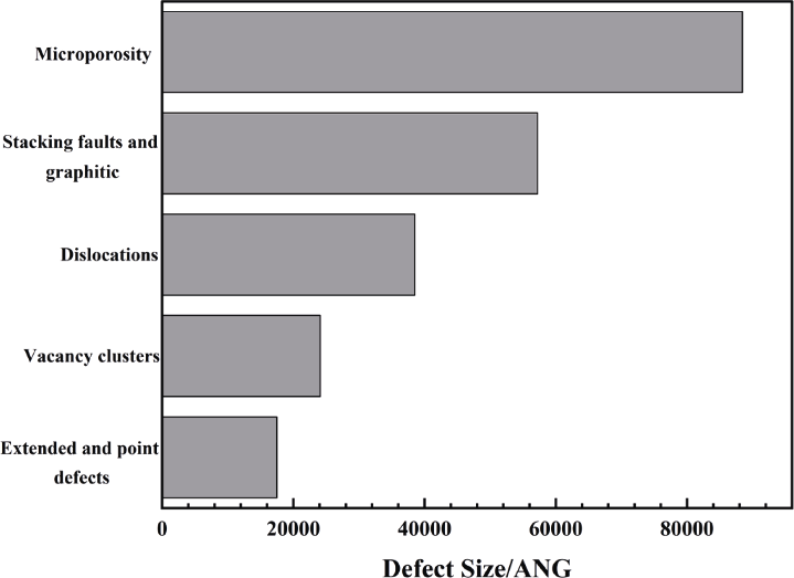
图1 不同种类缺陷尺寸对比[11]
Fig. 1 Comparison of different types of defect sizes[11]
| Substrate material | Elastic modulus/GPa | Melting temperature/K | Coefficient of thermal expansion (polynomial interpolation)/(×10-6, K-1) |
|---|---|---|---|
| Si | 130 | 1683 | -2.15+2.47×10⁻²T-3.82×10⁻⁵T2+2.67×10⁻⁸T3-6.87×10⁻¹²T4 |
| Mo | 327 | 2888 | 4.31+0.002T |
| W | 411 | 3660 | 2.78+0.01T-2.21×10⁻⁵T2+1.93×10⁻⁸T3-5.56×10⁻¹²T4 |
| Diamond | 1050 | — | -1.36+8.79×10⁻³T+3.98×10⁻⁷T²-6.18×10⁻⁹T³+2.78×10⁻¹²T4 |
表1 常见衬底材料的热膨胀系数[12]
Table 1 Thermal expansion coefficients of common substrate materials[12]
| Substrate material | Elastic modulus/GPa | Melting temperature/K | Coefficient of thermal expansion (polynomial interpolation)/(×10-6, K-1) |
|---|---|---|---|
| Si | 130 | 1683 | -2.15+2.47×10⁻²T-3.82×10⁻⁵T2+2.67×10⁻⁸T3-6.87×10⁻¹²T4 |
| Mo | 327 | 2888 | 4.31+0.002T |
| W | 411 | 3660 | 2.78+0.01T-2.21×10⁻⁵T2+1.93×10⁻⁸T3-5.56×10⁻¹²T4 |
| Diamond | 1050 | — | -1.36+8.79×10⁻³T+3.98×10⁻⁷T²-6.18×10⁻⁹T³+2.78×10⁻¹²T4 |
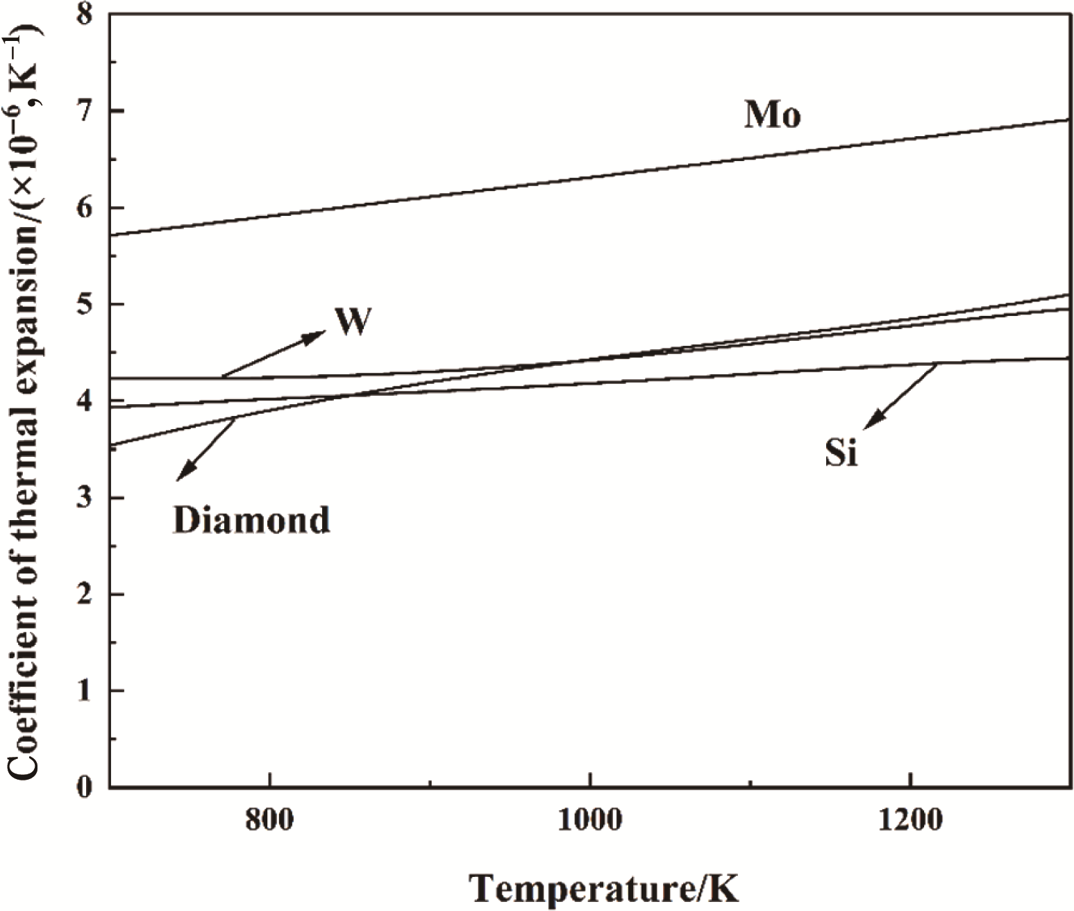
图2 常见衬底材料热膨胀系数与温度的关系[12]
Fig. 2 Relationship between coefficient of thermal expansion and temperature of common substrate materials[12]
| Material | Si (0.543 nm) | Mo (0.3147 nm) | W (0.3165 nm) | Diamond (0.357 nm) |
|---|---|---|---|---|
| Lattice mismatch | 34.3% | 13.4% | 12.8% | — |
表2 金刚石与各种材料的晶格常数及晶格错配度
Table 2 Lattice constants and lattice mismatch of diamond with various materials
| Material | Si (0.543 nm) | Mo (0.3147 nm) | W (0.3165 nm) | Diamond (0.357 nm) |
|---|---|---|---|---|
| Lattice mismatch | 34.3% | 13.4% | 12.8% | — |
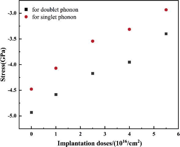
图3 碳离子注入剂量与应力的关系[47]
Fig. 3 Relationship between carbon ion implantation dose and stress[47]
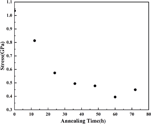
图4 退火时间与应力大小的关系[16]
Fig. 4 Relationship between annealing time and stress[16]
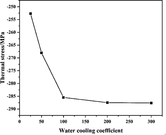
图5 水冷因数与热应力的关系[58]
Fig. 5 Relationship between water cooling coefficient and thermal stress[58]
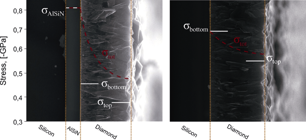
图6 系统的总应力σtot分布及Al-Si-N中间层应力σAlSiN, 金刚石膜底部应力σbottom和顶部应力σtop[62]
Fig. 6 Distribution of the total stress σtot in the system and the stress σAlSiN in the Al-Si-N intermediate layer, as well as the bottom and top stress (σbottom, σtop) of the diamond film[62]
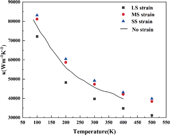
图7 不同尺度单轴拉伸应力下κ的温度依赖性[66]
Fig. 7 Temperature dependence of κ under uniaxial tensile stress at different scales[66]
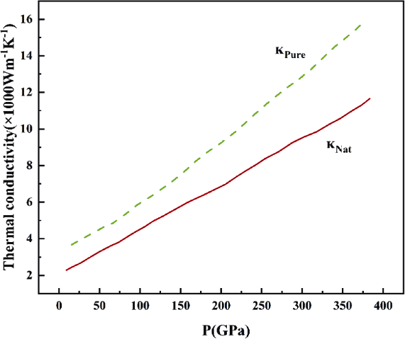
图8 300 K下天然金刚石和纯金刚石的热导率κNat和κPure随压力的变化[67]
Fig. 8 Thermal conductivity κNat and κPure of natural diamond and pure diamond varied with pressure at 300 K[67]
| [1] |
INYUSHKIN A V, TALDENKOV A N, RALCHENKO V G, et al. Thermal conductivity of high purity synthetic single crystal diamonds. Physical Review B, 2018, 97(14): 144305.
DOI URL |
| [2] | MARTIN H, REINTJES M, REIJS D, et al. Heterogeneous integration of diamond heat spreaders for power electronics application. IEEE 73rd Electronic Components and Technology Conference (ECTC), Orlando, 2023: 118-125. |
| [3] |
HOTCHANDANI V, MATHEW B, YESUDASAN S, et al. Thermo-hydraulic characteristics of novel MEMS heat sink. Microsystem Technologies, 2021, 27(1): 145.
DOI |
| [4] |
LEE V Y S, KARAYIANNIS T G. Effect of inlet subcooling on flow boiling in microchannels. Applied Thermal Engineering, 2020, 181: 115966.
DOI URL |
| [5] | SHAPIRA S, NIRENBERG N. Performance envelope enabled by CVD diamond heatspreader integration in semiconductor chips. IEEE International Conference on Microwaves, Communications, Antennas, Biomedical Engineering and Electronic Systems (COMCAS), Tel Aviv, 2024: 1-6. |
| [6] | SHAPIRA S. Performance enhancement of integrated circuits and power devices via embedded diamond heat management. IEEE International Conference on Microwaves, Antennas, Communications and Electronic Systems (COMCAS), Tel Aviv, 2021: 470-472. |
| [7] | LIU C. Stress response and physical properties of diamondunder complex strain. Changchun: PhD thesis of Jilin University, 2020. |
| [8] |
ZHANG S L, YE Z H, ZHU Y, et al. Enhanced optical properties of CVD diamond through HPHT annealing. Crystal Growth & Design, 2024, 24(16): 6701.
DOI URL |
| [9] |
FERREIRA N G, ABRAMOF E, CORAT E J, et al. Residual stresses and crystalline quality of heavily boron-doped diamond films analysed by micro-Raman spectroscopy and X-ray diffraction. Carbon, 2003, 41(6): 1301.
DOI URL |
| [10] | HUANG Y S, LOU C P, QIU W Q. Crystal defects and impurities of CVD diamond films. China Surface Engineering, 2004(1):5. |
| [11] | GRAY K J, WINDISCHMANN H. Free-standing CVD diamond wafers for thermal management by d.c. arc jet technology. Diamond & Related Materials, 1999, 8(2-5): 903. |
| [12] |
JEONG J H, LEE S Y, LEE W S, et al. Mechanical analysis for crack-free release of chemical-vapor-deposited diamond wafers. Diamond and Related Materials, 2002, 11(8): 1597.
DOI URL |
| [13] |
LEIGH W G S, CUENCA J A, THOMAS E L H, et al. Mapping the effect of substrate temperature inhomogeneity during microwave plasma-enhanced chemical vapour deposition nanocrystalline diamond growth. Carbon, 2023, 201: 328.
DOI URL |
| [14] | GEORGE C. Numerical simulation of a multicomponent non-transferred constricted direct current arc with a supersonic plasma jet. Minnesota: PhD thesis of University of Minnesota, 1998. |
| [15] | FAN Y D, ZHOU Z F. Crystal defects and impurities of CVD diamond films. Journal of Materials Science and Engineering (Materials Science & Engineering), 1996(1): 5. |
| [16] | NAKAMURA Y, SAKAGAMI S, AMAMOTO Y, et al. Measurement of internal stresses in CVD diamond films. Thin Solid Films, 1997, 308: 249. |
| [17] | SCARDI P, LEONI M, SESSA V, et al. Residual stress in diamond coatings by synchrotron radiation XRD. European Powder Diffraction: Epdic Iv, Pts 1 and 2, Stafa-Zurich, 1996: 451-456. |
| [18] |
WENG J, LIU F, XIONG L W, et al. Deposition of large area uniform diamond films by microwave plasma CVD. Vacuum, 2018, 147: 134.
DOI URL |
| [19] |
SCHRECK M, BAUR T, FEHLING R, et al. Modification of diamond film growth by a negative bias voltage in microwave plasma chemical vapor deposition. Diamond and Related Materials, 1998, 7(2-5): 293.
DOI URL |
| [20] |
LIU P, SHAO S, YANG Z, et al. The uniform and robust 8-inch CVD diamond plate generated by dual-magnetic field controlled DC Jet CVD. Diamond and Related Materials, 2024, 141: 110670.
DOI URL |
| [21] |
HUANG Y, CHEN L, SHAO S, et al. The 7-in. freestanding diamond thermal conductive film fabricated by DC arc plasma jet CVD with multi-stage magnetic fields. Diamond and Related Materials, 2022, 122: 108812.
DOI URL |
| [22] |
FERREIRA N G, ABRAMOF E, LEITE N F, et al. Analysis of residual stress in diamond films by X-ray diffraction and micro-Raman spectroscopy. Journal of Applied Physics, 2002, 91(4): 2466.
DOI URL |
| [23] |
LONG F, WEI Q P, YU Z M, et al. Effects of temperature and Mo2C layer on stress and structural properties in CVD diamond film grown on Mo foil. Journal of Alloys and Compounds, 2013, 579: 638.
DOI URL |
| [24] |
WOEHRL N, HIRTE T, POSTH O, et al. Investigation of the coefficient of thermal expansion in nanocrystalline diamond films. Diamond and Related Materials, 2009, 18(2/3): 224.
DOI URL |
| [25] | YANG J X, LI C M, CHEN G C, et al. Analysis of residual stress distribution in DC arc plasma jet CVD high quality diamond films by Raman spectroscopy. Journal of Synthetic Crystals, 2004(4): 674. |
| [26] | DAI X N, BAI L, SUN W Y, et al. Study on the preparation technology of diamond film by MPCVD. Superhard Material Engineering, 2022, 34(2): 36. |
| [27] |
WOEHRL N, BUCK V. Influence of hydrogen on the residual stress in nanocrystalline diamond films. Diamond and Related Materials, 2007, 16(4-7): 748.
DOI URL |
| [28] | YAMADA H. Numerical simulations to study growth of single- crystal diamond by using microwave plasma chemical vapor deposition with reactive (H, C, N) species. Japanese Journal of Applied Physics, 2012, 51(9): 105. |
| [29] | LIANG T. Study on high quality diamond prepared by high pressure MPCVD. Wuhan: Master Thesis of Wuhan Institute of Technology, 2018. |
| [30] |
SALGUEIREDO E, AMARAL M, NETO M A, et al. HFCVD diamond deposition parameters optimized by a Taguchi Matrix. Vacuum, 2011, 85(6): 701.
DOI URL |
| [31] | ZHU H X, MAO W M, FENG H P. Influence of texture on residual strain in CVD free standing diamond films. Chinese Journal of Materials Research, 2007(1): 32. |
| [32] | ZHOU Z Y, CHEN G C, ZHOU Y L, et al. Controlling deposition and roughness of free-standing diamond film deposited by DC plasma jet CVD. Journal of Synthetic Crystals, 2005(1): 21. |
| [33] | LI R B. Study of the stress in doped CVD diamond films. Acta Physica Sinica, 2007(6): 3428. |
| [34] |
MAO W M, ZHU H X, CHEN L, et al. Relationship between texture and residual macro-strain in CVD diamond films based on phenomenological analysis. Journal of University of Science and Technology Beijing, 2008, 15(2): 197.
DOI URL |
| [35] |
IKEDA R, UCHIYAMA T, CHO H, et al. An advanced method for measuring the residual stress of deposited film utilizing laser spallation technique. Science and Technology of Advanced Materials, 2006, 7(1): 90.
DOI URL |
| [36] |
TSUJI T, SHINEI C, IWASAKI T, et al. Evaluation of stress in (111) homoepitaxial CVD diamond films by Raman spectrum and nitrogen- vacancy centers. Applied Physics Express, 2024, 17(11): 115502.
DOI |
| [37] | HE J S, ZHANG M, XIAO Q. Calculation of the lattice mismatch between semiconductor epitaxy and substrate. Journal of Nanchang University Natural Science, 2006, 30(1): 63. |
| [38] | NIU D C, LI C M, LIU Z, et al. Growth stability and quality of plasma jet CVD diamond films under gas recycling condition. Journal of University Science and Technology Beijing, 2007, 29(11): 1133. |
| [39] |
TACHIBANA T, YOKOTA Y, HAYASHI K, et al. Parametric study of bias-enhanced nucleation of diamond on platinum in microwave plasma. Diamond and Related Materials, 2000, 9(3-6): 251.
DOI URL |
| [40] |
NIU C M, TSAGAROPOULOS G, BAGLIO J, et al. Nucleation and growth of diamond on Si, Cu, and Au substrates. Journal of Solid State Chemistry, 1991, 91(1): 47.
DOI URL |
| [41] |
CHIU K A, WU P H, WANG W L, et al. Homoepitaxial overgrowth of (111) diamond films on Au-coated and Ni-coated substrates. Surface and Coatings Technology, 2022, 437: 128348.
DOI URL |
| [42] |
KHAN M A, HAQUE M S, NASEEM H A, et al. Microwave plasma chemical vapor deposition of diamond films with low residual stress on large area porous silicon substrates. Thin Solid Films, 1998, 332(1/2): 93.
DOI URL |
| [43] | ZHANG Y Y, ZHANG D L, ZHANG L B, et al. The effect of surface roughness of seed on the high-rate homoepitaxial growth of CVD single-crystal diamonds. Applied Physics A-Materials Science & Processing, 2023, 129(6): 415. |
| [44] |
SILVA F, ACHARD J, BRINZA O, et al. High quality, large surface area, homoepitaxial MPACVD diamond growth. Diamond and Related Materials, 2009, 18(5-8): 683.
DOI URL |
| [45] | MARTINEAU P M, LAWSON S C, TAYLOR A J, et al. Identification of synthetic diamond grown using chemical vapor deposition (CVD). Gems & Gemology, 2004, 40(1): 2. |
| [46] |
GAUKROGER M P, MARTINEAU P M, CROWDER M J, et al. X-ray topography studies of dislocations in single crystal CVD diamond. Diamond and Related Materials, 2008, 17(3): 262.
DOI URL |
| [47] | XIA Y B, WANG L J. Diamond film/alumina composites used as the packaging material in integrated circuits with ultra-high speed and high power. 6th IEEE CPMT Conference on High Density Microsystem Design and Packaging and Component Failure Analysis (HDP 04), Shanghai, 2004: 367-372. |
| [48] |
ITO S, NAGAI M, MATSUMOTO T, et al. Self-separation of freestanding diamond films using graphite interlayers precipitated from C-dissolved Ni substrates. Journal of Crystal Growth, 2017, 470: 104.
DOI URL |
| [49] |
MATTHIEU J. VERSTRAETE J C C. Why is iridium the best substrate for single crystal diamond growth? Applied Physics Letters, 2005, 86(191): 191917.
DOI URL |
| [50] | REDDY P R S, JANARDHANAM V, REDDY V R, et al. Effects of rapid thermal annealing on the structural, optical, and electrical properties of Au/CuPc/n-Si (MPS)-type Schottky barrier diodes. Applied Physics A-Materials Science & Processing, 2021, 127(10): 803. |
| [51] | PAVANI M, KUMAR A A, REDDY V R, et al. Optical, morphological and electrical properties of rapid thermally annealed CoPc/n-Ge heterostructures for photodiode applications. Materials Science and Engineering B-Advanced Functional Solid-State Materials, 2024, 300: 117102. |
| [52] |
FENG C Q, WU L, CHEN P, et al. Repairing slight damages on monocrystalline silicon surface by thermal annealing. Materials Research Express, 2021, 8(4): 045005.
DOI |
| [53] |
WU J M, HE Z, GUO Z Y, et al. Pulsed laser annealing of phosphorous-implanted 4H-SiC: electrical and structural characteristics. Journal of Electronic Materials, 2022, 51(1): 172.
DOI |
| [54] |
YANG T, XIA Z L, FAN D Y, et al. Activation enhancement and grain size improvement for poly-Si channel vertical transistor by laser thermal annealing in 3D NAND Flash. Micromachines, 2023, 14(1): 230.
DOI URL |
| [55] |
JACOBS A G, FEIGELSON B N, SPENCER J A, et al. Efficient activation and high mobility of ion-implanted silicon for next-generation GaN devices. Crystals, 2023, 13(5): 736.
DOI URL |
| [56] | NIJHAWAN S, RANKIN J, WALDEN B L, et al. Grain impingement and intrinsic stresses in CVD diamond. Symposium on Thin-Films-Stresses and Mechanical Properties VII at the MRS Fall Meeting, Boston, 1997: 415-420. |
| [57] | YAN X B. Graphitization behavior of CVD free-standing diamond films at high temperature. Beijing: PhD thesis of University of Science &Technology Beijing, 2019. |
| [58] | XU F, ZUO D W, LU W Z, et al. Study of the thermal and intrinsic stress of large area diamond film prepared by HFCVD. 9th Conference on Machining and Advanced Manufacturing Technology in China, Harbin, 2007: 123-127. |
| [59] | YANG C, LIU D, ZHU F, et al. Method for reducing crack of diamond film, involves controlling substrate column to be separated from cooling table placed under substrate column until cooling is completed, in cooling process after growth is completed, when temperature of substrate column is lowered to set temperature: CN113684466-A; CN113684466-B. 2021-11-23; 2022-01-25. |
| [60] |
CHANG Y Y, YANG Y J, WENG S Y. Effect of interlayer design on the mechanical properties of AlTiCrN and multilayered AlTiCrN/ TiSiN hard coatings. Surface & Coatings Technology, 2020, 389: 125637.
DOI URL |
| [61] |
LIU L L, RUAN Q D, WU Z Z, et al. Fabrication and cutting performance of CrAlN/CrAl multilayer coatings deposited by continuous high-power magnetron sputtering. Ceramics International, 2022, 48(10): 14528.
DOI URL |
| [62] |
GAYDAYCHUK A, ZENKIN S, LINNIK S. Influence of Al-Si-N interlayer on residual stress of CVD diamond coatings. Surface & Coatings Technology, 2019, 357: 348.
DOI URL |
| [63] | DU Y, YAN B, LI H, et al. Method for preparing low stress diamond film by using ultrasonic cavitation technology to synthesize metal gallium buffer layer in medical fields, involves adding liquid gallium into ethanol, performing ultrasonic treatment, and taking supernatant to obtain metal gallium nano-particle suspension: CN117026201-A. 2023-11-10. |
| [64] |
GUO J C, LIU J L, HUA C Y, et al. Interfacial stress evolution simulation on the graphite substrate/interlayer/diamond film during the cooling process. Diamond and Related Materials, 2017, 75: 12.
DOI URL |
| [65] | RILEY P R, JOSHI P, NARAYAN J, et al. Enhanced nucleation and large-scale growth of CVD diamond via surface-modification of silicon-incorporated diamond-like carbon thin films. Diamond and Related Materials, 2021, 120: 11. |
| [66] | WANG B, ZHAO J W, HU Y W, et al. Anomalous thermal response of bulk diamond to uniaxial (100) strain: a first-principles prediction. Physical Review B, 2022, 106(18): 10. |
| [67] | BROIDO D A, LINDSAY L, WARD A. Thermal conductivity of diamond under extreme pressure: a first-principles study. Physical Review B, 2012, 86(11): 7. |
| [68] |
LIU C, SONG X Q, LI Q, et al. Superconductivity in compression-shear deformed diamond. Physical Review Letters, 2020, 124(14): 147001.
DOI URL |
| [69] |
DANG C Q, CHOU J P, DAI B, et al. Achieving large uniform tensile elasticity in microfabricated diamond. Science, 2021, 371(6524): 76.
DOI PMID |
| [70] |
NIE A M, BU Y Q, LI P H, et al. Approaching diamond's theoretical elasticity and strength limits. Nature Communications, 2019, 10: 7.
DOI |
| [71] |
LIU Z, LI C M, NIU D C, et al. Finite-element analysis of thermal stresses in diamond film deposition on Mo substrate with Ti interlayer. Materials Science Forum, 2008, 575-578: 996.
DOI URL |
| [72] |
SHAO S, LIU P, YE S, et al. Structural evolution and self- destructive behavior of Mo/Ti transition layers during free- standing diamond-film preparation. Ceramics International, 2024, 50(13): 23677.
DOI URL |
| [73] |
YULIANTO N, KADJA G T M, BORNEMANN S, et al. Ultrashort pulse laser lift-off processing of InGaN/GaN light-emitting diode chips. ACS Applied Electronic Materials, 2021, 3(2): 778.
DOI URL |
| [74] | ZHANG J, ZHANG W. Micro-LED laser lift-off research of GaN on AlN of sapphire substrate. Laser Technology, 2023, 47(1): 25. |
| [75] |
QIN F F, ZHU Q X, ZHANG Y F, et al. Effect of substrates on lasing properties of GaN transferable membranes. Optical Materials, 2021, 122: 111663.
DOI URL |
| [76] |
PIÑERO J C, FERNÁNDEZ D, LLORET F, et al. Inducing controlled blistering by Smart-Cut™ process in semiconducting diamond: a STEM study. Applied Surface Science, 2025, 681: 161570.
DOI URL |
| [77] |
MASANTE C, DE VECCHY J, MAZEN F, et al. Hydrogen implantation-induced blistering in diamond: toward diamond layer transfer by the Smart Cut™ technique. Diamond and Related Materials, 2022, 126: 109085.
DOI URL |
| [78] |
JING J X, SUN F Q, WANG Z Q, et al. Scalable production of ultraflat and ultraflexible diamond membrane. Nature, 2024, 636(8043): 627.
DOI |
| [79] | LI Y, XU J Q, SU J H, et al. Residual stress and deformation of 1064 nm high reflection films for laser systems. Surface Technology, 2022, 51(9): 311. |
| [80] |
PENG X L, TSUI Y C, CLYNE T W. Stiffness, residual stresses and interfacial fracture energy of diamond films on titanium. Diamond and Related Materials, 1997, 6(11): 1612.
DOI URL |
| [81] |
CHEN S L, SHEN B, ZHANG J G, et al. Evaluation on residual stresses of silicon-doped CVD diamond films using X-ray diffraction and Raman spectroscopy. Transactions of Nonferrous Metals Society of China, 2012, 22(12): 3021.
DOI URL |
| [82] |
AHMED F, BAYERLEIN K, ROSIWAL S M, et al. Stress evolution and cracking of crystalline diamond thin films on ductile titanium substrate: analysis by micro-Raman spectroscopy and analytical modelling. Acta Materialia, 2011, 59(14): 5422.
DOI URL |
| [83] |
SHU G Y, DAI B, RALCHENKQ V G, et al. Epitaxial growth of mosaic diamond: mapping of stress and defects in crystal junction with a confocal Raman spectroscopy. Journal of Crystal Growth, 2017, 463: 19.
DOI URL |
| [84] |
BOPPART H, VAN STRAATEN J, SILVERA I F. Raman spectra of diamond at high pressures. Physical Review B, 1985, 32(2): 1423.
PMID |
| [85] |
TARDIEU A, CANSELL F, PETITET J P. Pressure and temperature dependence of the first-order Raman mode of diamond. Journal of Applied Physics, 1990, 68(7): 3243.
DOI URL |
| [86] |
DURAND O, BISARO R, BRIERLEY C J, et al. Residual stresses in chemical vapor deposition free-standing diamond films by X-ray diffraction analyses. Materials Science and Engineering A, 2000, 288(2): 217.
DOI URL |
| [87] | Shanghai Research Institute of Materials. Non-destructive testing—practice for residual stress measurement by X-ray: GB/T 7704--2017. Beijing: Standards Press of China, 2017. |
| [88] | AIDA H, IHARA T, OSHIMA R, et al. Analysis of external surface and internal lattice curvatures of freestanding heteroepitaxial diamond grown on an Ir (001)/MgO (001) substrate. Diamond and Related Materials, 2023, 136: 9. |
| [89] |
LI Z, CUI C, ARTEAGA O, et al. Full-field measurement of residual stress in single-crystal diamond substrates based on Mueller matrix microscopy. Measurement, 2024, 234: 114790.
DOI URL |
| [90] |
HUA C Y, YAN X B, WEI J J, et al. Intrinsic stress evolution during different growth stages of diamond film. Diamond and Related Materials, 2017, 73: 62.
DOI URL |
| [91] |
SRIKANTH V, STAEDLER T, JIANG X. Deposition of stress-free diamond films on Si by diamond/β-SiC nanocomposite intermediate layers. Diamond and Related Materials, 2009, 18(10): 1326.
DOI URL |
| [92] | North University of China. Micro-electromechanical system technology—measuring method of microstructure surface stress based on Raman spectroscopy: GB/T 34899- -2017. Beijing: Standards Press of China, 2017. |
| [93] |
CHAN S Y, TU J P, HUANG K, et al. Oriented growth of 5-inch optical polycrystalline diamond films by suppressing dark features. Ceramics International, 2024, 50(19): 37111.
DOI URL |
| [94] |
LIN H, LI J, YANG Z L, et al. Recent progress in stress analysis technology and application of neutron diffraction. Acta Metallurgica Sinica, 2024, 60(8): 1017.
DOI |
| [1] | 陈明俊, 缪洪康, 肖英俊, 邓建波, 张翔, 赵九蓬, 李垚. 光-热双响应材料研究进展: 从设计策略到智能窗应用[J]. 无机材料学报, 2026, 41(6): 723-738. |
| [2] | 宋坤洁, 解荣军. 机器学习驱动新型发光材料的研究进展[J]. 无机材料学报, 2026, 41(6): 689-703. |
| [3] | 胡钰晴, 朱一新, 乐先浩, 万青. 钽酸锂晶圆减薄技术及其热释电红外探测器应用进展[J]. 无机材料学报, 2026, 41(6): 764-774. |
| [4] | 刘春帆, 陈科, 葛芳芳, 黄庆. 核用耐铅铋腐蚀涂层的研究进展[J]. 无机材料学报, 2026, 41(6): 775-786. |
| [5] | 胡扬, 谢敏, 张筱怡, 李想, 郭新伟, 姜南, 周文瀚, 张胜利, 曾海波. 计算与数据驱动环保型发光材料的研究进展[J]. 无机材料学报, 2026, 41(6): 704-722. |
| [6] | 王俊卜, 黄泽皑, 杨茗凯, 蒙颖, 周明炜, 周莹. 甲烷转化用抗积碳催化材料研究进展[J]. 无机材料学报, 2026, 41(6): 739-750. |
| [7] | 王金文, 杨振, 周欢, 夏丹, 杨磊. 可注射无机材料及其生物医学应用[J]. 无机材料学报, 2026, 41(6): 751-763. |
| [8] | 李涵涛, 沈强, 罗国强, 王雪飞, 高明, 陈晨. 机械球磨法调控硅基负极材料结构与性能的研究进展[J]. 无机材料学报, 2026, 41(5): 561-572. |
| [9] | 解陈一, 缪花明, 张蔚然, 刘荣军, 王衍飞, 李端. 理论计算在高熵陶瓷领域的研究进展[J]. 无机材料学报, 2026, 41(5): 545-560. |
| [10] | 李璇, 叶奎材, 冯佳音, 邱家军, 钱文昊, 邢敏. 钛基牙种植体表面改性促进软组织封闭的研究进展[J]. 无机材料学报, 2026, 41(4): 432-444. |
| [11] | 彭德招, 李瑞, 王文鸿, 王梓瑞, 章志珍. 钠氯化物固态电解质研究进展[J]. 无机材料学报, 2026, 41(4): 409-420. |
| [12] | 陈坤, 姜勇刚, 冯军宗, 李良军, 胡艺洁, 冯坚. 锆酸镧多孔隔热材料研究进展[J]. 无机材料学报, 2026, 41(4): 421-431. |
| [13] | 韦连金, 齐志杰, 汪信, 朱俊武, 付永胜. 纳米金刚石改性及其在电催化氧还原反应中的应用[J]. 无机材料学报, 2026, 41(3): 273-288. |
| [14] | 刘占一, 李勉, 欧阳晓平, 柴之芳, 黄庆. 干法后处理熔盐中Sr/Cs去除方法的研究进展[J]. 无机材料学报, 2026, 41(2): 150-158. |
| [15] | 孙炼, 张磊磊, 薛泽旭, 吴坤, 陈晔, 李志远, 王鲁凯, 王尊刚. 面向辐射探测应用的零维金属卤化物闪烁体研究进展[J]. 无机材料学报, 2026, 41(2): 159-176. |
| 阅读次数 | ||||||
|
全文 |
|
|||||
|
摘要 |
|
|||||