ISSN:1000-324X CN:31-1363/TQ
高级检索
图表检索
导航切换
无机材料学报
首页
期刊介绍
刊物介绍
编委会
数据库收录
影响因子
青年编委会
读者中心
最新录用
当期目录
过刊浏览
阅读排行
下载排行
征订启事
作者中心
作者投稿
作者指南
下载中心
审稿中心
编委登录
专家审稿
主编办公
编辑办公
精彩推荐
专辑文章
热点文章
虚拟专题
封面文章
联系方式
Email Alert
English
图/表 说明
高级检索
期刊
DOI
请选择
无机材料学报
起始年
结束年
请选择
1997
1998
1999
2000
2001
2002
2003
2004
2005
2006
2007
2008
2009
2010
2011
2012
2013
2014
2015
2016
2017
2018
2019
2020
2021
2022
2023
2024
2025
请选择
2025
2024
2023
2022
2021
2020
2019
2018
2017
2016
2015
2014
2013
2012
2011
2010
2009
2008
2007
2006
2005
2004
2003
2002
2001
2000
1999
1998
1997
卷
期
作者
作者单位
期刊
出版年
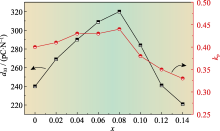
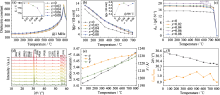
Fig. 7
d
33
and
k
p
of (1-
x
)(0.8PZT-0.2PZN)-
x
BZT ceramics
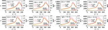
Fig. 6
Temperature dependence of
ε
r
and tan
δ
of (1-
x
)(0.8PZT-0.2PZN)-
x
BZT ceramics
(a)
x
=0; (b)
x
=0.02; (c)
x
=0.04; (d)
x
=0.06; (e)
x
=0.08; (f)
x
=0.10; (g)
x
=0.12; (h)
x
=0.14. Colorful figures are available on website
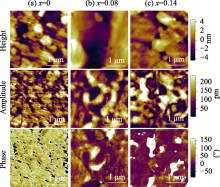
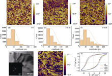
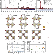
Fig. 5
Room temperature out-of-plane height, amplitude, and phase images of (1-
x
)(0.8PZT-0.2PZN)-
x
BZT ceramics
(a)
x
=0; (b)
x
=0.08; (c)
x
=0.14. Colorful figures are available on website
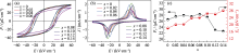
Fig. 4
P-E
hysteresis loops (a),
J-E
curves (b) and variation trends of the remnant polarization
P
r
and coercive field
E
c
(c) for (1-
x
)(0.8PZT-0.2PZN)-
x
BZT ceramics at room temperature
Colorful figures are available on website
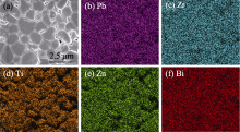
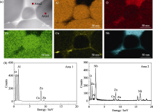
Fig. 3
Microstructure (a) and element mappings (b-f) of (1-
x
)(0.8PZT-0.2PZN)-
x
BZT (
x
=0.08) ceramics
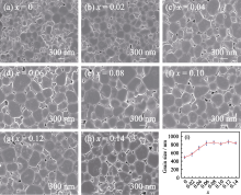
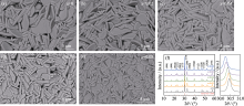
Fig. 2
SEM images (a-h) and average grain sizes (i) of (1-
x
)(0.8PZT-0.2PZN)-
x
BZT ceramics
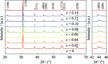
Fig. 1
XRD patterns of (1-
x
)(0.8PZT-0.2PZN)-
x
BZT ceramics
Fig. 7
PFM characterization of CBT-
x
Bi ceramics
(a-c) PFM phase images for (a)
x
=0, (b)
x
=0.04, and (c)
x
=0.06; (d-f) PFM amplitude distribution histograms for (d)
x
=0, (e)
x
=0.04, and (f)
x
=0.06; (g) TEM image of CBT-0.06Bi; (h) 5 μm×5 μm PFM phase image of CBT-0.06Bi; (i) Hysteresis loops of CBT-
x
Bi ceramics after polarizing at 180 ℃ and 1 Hz. Colorful figures are available on website
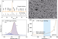
Fig. 6
(a) XRD refinement results of CBT-
x
Bi ceramics; (b) Visual crystal structures of CBT-
x
Bi ceramics; (c) Raman scattering spectra in the range of 80-900 cm
-1
; (d) Wavenumber displacements of B
2g
, B
3g
, A
1g
, and B
1g
modes
Fig. 5
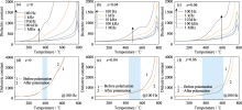
(a) Dielectric temperature spectra of CBT-
x
Bi ceramics; (b) Temperature dependence of DC resistivity of CBT-
x
Bi ceramics; (c) Effect of heat treatment on the piezoelectric constants of CBT-
x
Bi ceramics (set temperature annealing 2 h); (d)
In-situ
XRD patterns of CBT-0.06Bi ceramic; (e) Relationship between lattice constants and unit cell volume with temperature; (f) (119) peak position and
I
(200)
/
I
(020)
changed with temperature
Fig. 4
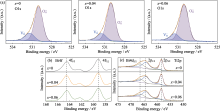
Characterization of CBT-0.06Bi ceramic sintered in a flowing oxygen atmosphere
(a) XRD patterns; (b) SEM image of the thermal etching surface; (c) O1s XPS spectrum; (d) Dielectric temperature spectra at 100 Hz before and after polarization
Table 1 Results of CBT-xBi ceramics O1s XPS peak fitting analysis
Fig. 3
XPS core-level spectra of CBT-
x
Bi ceramics
(a) O1s; (b) Bi4f; (c) Bi4d
3/2
and Ti2p
Fig. 2
Dielectric properties of CBT-
x
Bi ceramics
(a-c) Dielectric constant as a function of temperature at different frequencies after polarization: (a)
x
=0, (b)
x
=0.04 and (c)
x
=0.06; (d-f) Dielectric constant as a function of temperature at 100 Hz before and after polarization: (d)
x
=0, (e)
x
=0.04 and (f)
x
=0.06
Fig. 1
(a-e) Surface SEM images of CBT-
x
Bi ceramics after thermal etching; (f) XRD patterns of CBT-
x
Bi ceramics and corresponding localized enlarged patterns
(a)
x
=0; (b)
x
=0.02; (c)
x
=0.04; (d)
x
=0.06; (e)
x
=0.08
Table S2 EDS analysis results for the grain (Area 1) and the adjacent second phase (Area 2)
Fig. S4
EDS element mappings of sample S5 sintered at 975 ℃ for 2 h (a) and EDS spectra of the grain phase (Area 1) and the adjacent second phase (Area 2) (b)
Fig. S3
XPS spectra of sample S5 sintered at 1000 ℃ for 2 h (a) and detailed XPS spectra of Cu ion (b), Nb ion (c) and O1s (d)
Fig. S2
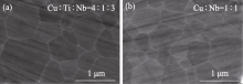
Backscattered electron SEM images of the fracture surface of samples S4 and S5
Table S1 Properties of ZnAl
2
O
4
ceramics with different formulas of CTN additives
跳至
页
第1页
共989页
共19776条记录
首页
上一页
下一页
尾页