无机材料学报 ›› 2026, Vol. 41 ›› Issue (2): 253-261.DOI: 10.15541/jim20250076 CSTR: 32189.14.jim20250076
邓恒杨1( ), 秦翠洁1, 郝胜兰1, 冯光迪1,2, 朱秋香1(), 田博博1,2(), 褚君浩1, 段纯刚1,3
收稿日期:2025-02-22
修回日期:2025-03-14
出版日期:2026-02-20
网络出版日期:2025-05-09
通讯作者:
朱秋香, 副教授. E-mail: qxzhu@clpm.ecnu.edu.cn;作者简介:邓恒杨(1999-), 男, 硕士研究生. E-mail: 51254700083@stu.ecnu.edu.cn
DENG Hengyang1(), QIN Cuijie1, HAO Shenglan1, FENG Guangdi1,2, ZHU Qiuxiang1(), TIAN Bobo1,2(), CHU Junhao1, DUAN Chungang1,3
Received:2025-02-22
Revised:2025-03-14
Published:2026-02-20
Online:2025-05-09
Contact:
ZHU Qiuxiang, associate professor. E-mail: qxzhu@clpm.ecnu.edu.cn;About author:DENG Hengyang (1999-), male, Master candidate. E-mail: 51254700083@stu.ecnu.edu.cn
Supported by:摘要:
隧穿二极管在太赫兹(THz)和可见光频谱的未来整流领域中具有显著的应用前景, 这得益于其拥有飞秒级的隧穿渡越时间。本研究制备了隧穿距离分别为10和5 nm的TiN/ZnO/Pt鳍式隧道二极管(Fin tunneling diodes, FTDs), 它们展现出优异的特性, 其中包括超高的不对称性(10 nm器件为1.6×10⁴, 5 nm器件为1.6×10³)、零偏压下的高响应度(10 nm器件为25.3 V-1, 5 nm器件为28.3 V-1), 均超越了传统肖特基二极管的热电压限制, 并且两个器件的开启电压(Von)都极低, 约为100 mV, 这使得它们成为能量转换应用的理想选择。基于技术计算机辅助设计(Technology computer-aided design, TCAD)模拟, 所观测到的电子传输不对称性可归因于在不同偏置条件下福勒-诺德海姆隧穿(Fowler-Nordheim tunneling, FNT)和陷阱辅助隧穿(Trap-assisted tunneling, TAT)之间的转变, 这在相应的能带排列图中得以阐明。此外, 通过对FTDs进行集成, 设计了一种具有全波整流特性的整流桥电路, 其在太赫兹波段(0.1 THz)的整流性能通过SPICE电路仿真得到了验证。本研究为太赫兹能量转换和探测应用提供了一种高效的解决方案。
中图分类号:
邓恒杨, 秦翠洁, 郝胜兰, 冯光迪, 朱秋香, 田博博, 褚君浩, 段纯刚. 基于金属-半导体-金属鳍式隧穿二极管的高频整流桥电路[J]. 无机材料学报, 2026, 41(2): 253-261.
DENG Hengyang, QIN Cuijie, HAO Shenglan, FENG Guangdi, ZHU Qiuxiang, TIAN Bobo, CHU Junhao, DUAN Chungang. A Rectifier Bridge Circuit Based on Metal-semiconductor-metal Fin Tunneling Diode for High-frequency Application[J]. Journal of Inorganic Materials, 2026, 41(2): 253-261.
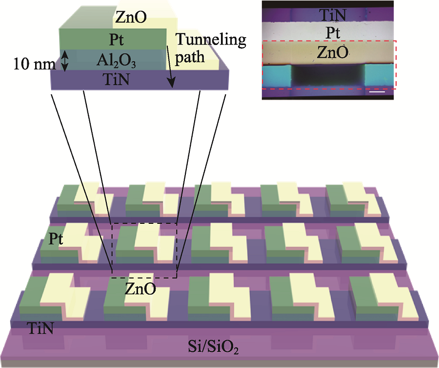
Fig. 1 Schematic diagram of line array constituted by TiN/ZnO/Pt FTDs fabricated on a Si/SiO2 substrate, along with cross-sectional view of a single device Upper right inset shows an optical image of an individual device from the top view (scale: 100 μm)
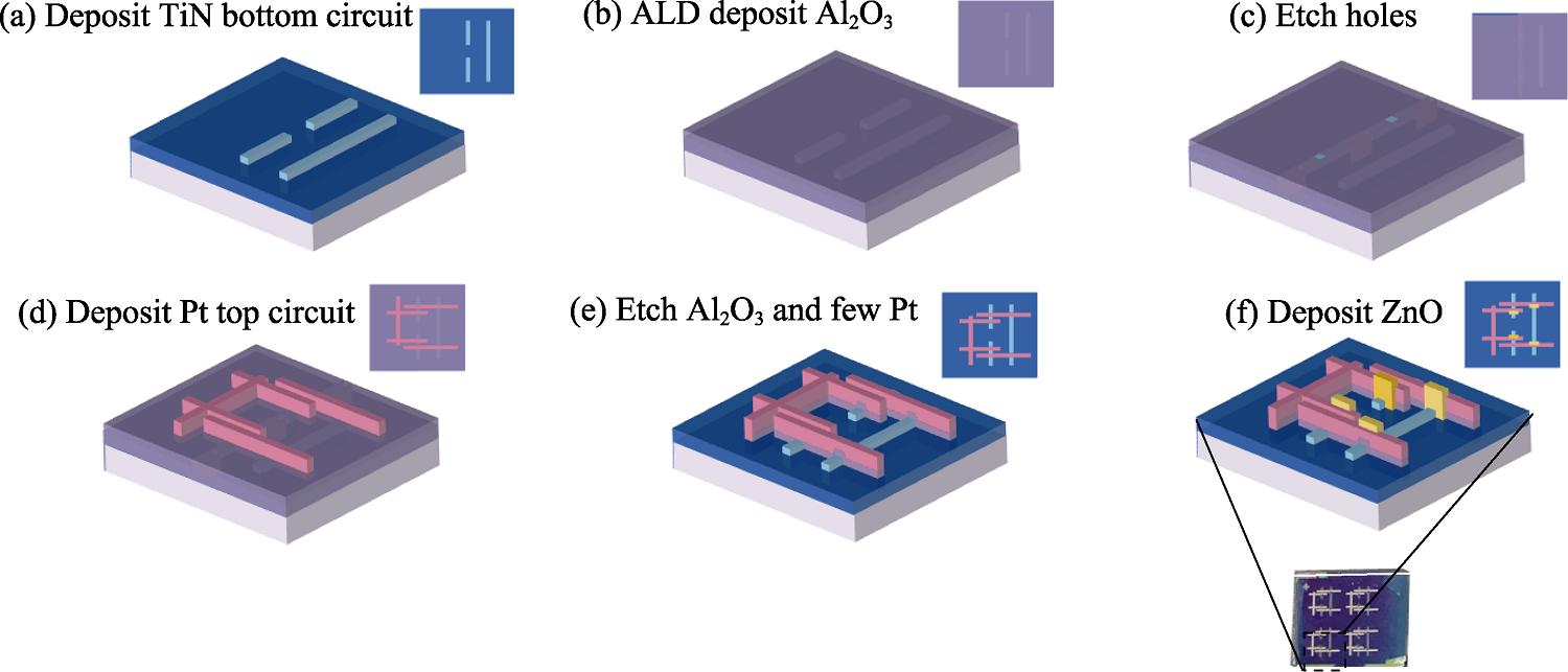
Fig. 2 Fabrication process of the rectifier bridge (a) Deposit TiN bottom circuit; (b) ALD (Atomic layer deposition) deposit Al2O3; (c) Etch holes; (d) Deposit Pt top circuit; (e) Etch Al2O3 and few Pt; (f) Deposit ZnO
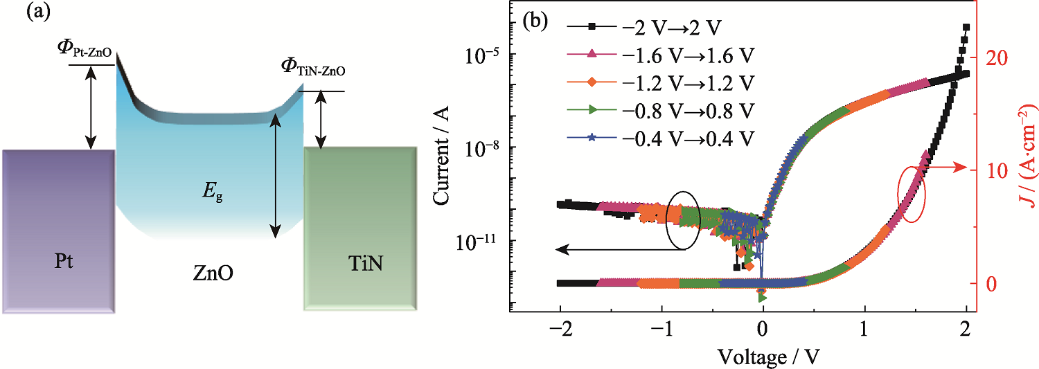
Fig. 3 Energy band alignments and electrical characteristics (a) Energy band alignments of ZnO and electrodes (Pt and TiN) after contact; (b) I-V and J-V characteristics of the TiN/ZnO/Pt FTD device across various bias voltage ranges, where the bias is applied to the bottom electrode (TiN) and the top electrode (Pt) remains grounded
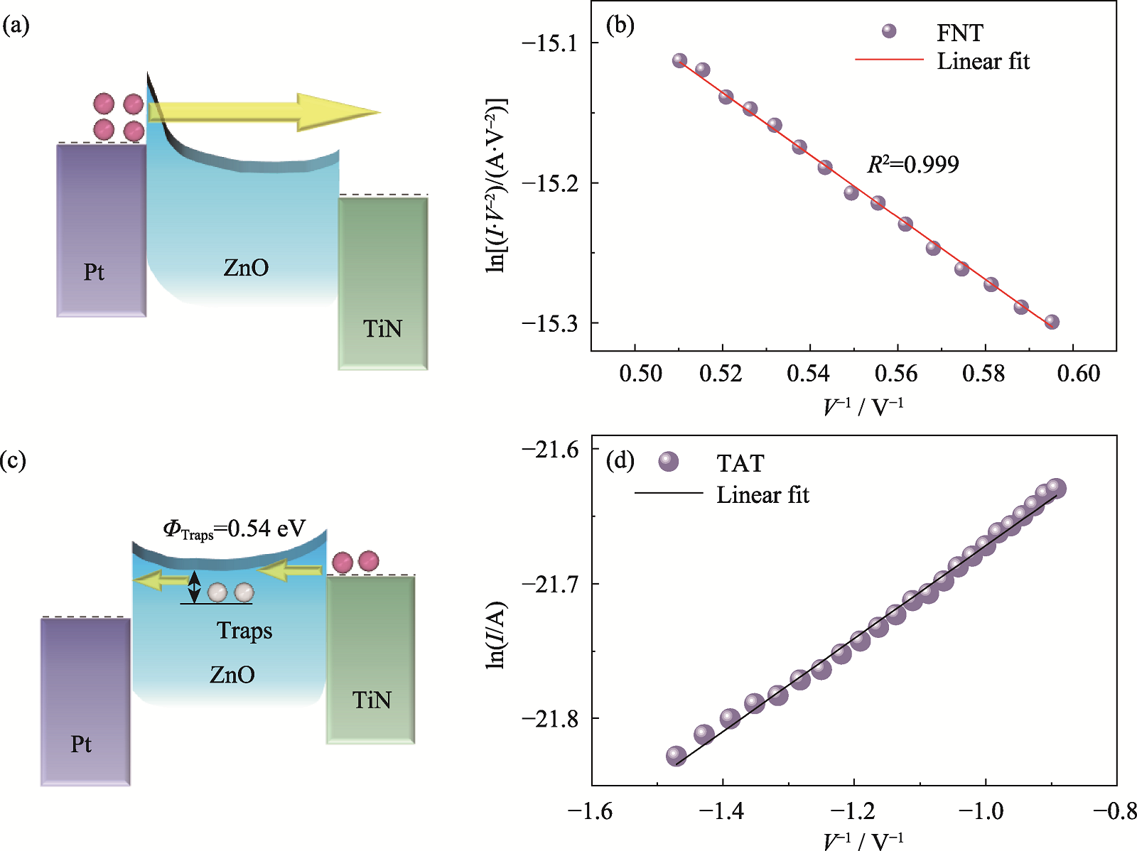
Fig. 4 Energy band alignments and fitting of tunneling mechanism of the FTD (a) Energy band alignments of the FTD and (b) ln(I/V2) vs. V-1 plots with FNT fitting under positive voltage; (c) Energy band alignments of the FTD and (d) lnI vs. V-1 plots with TAT fitting under negative voltage
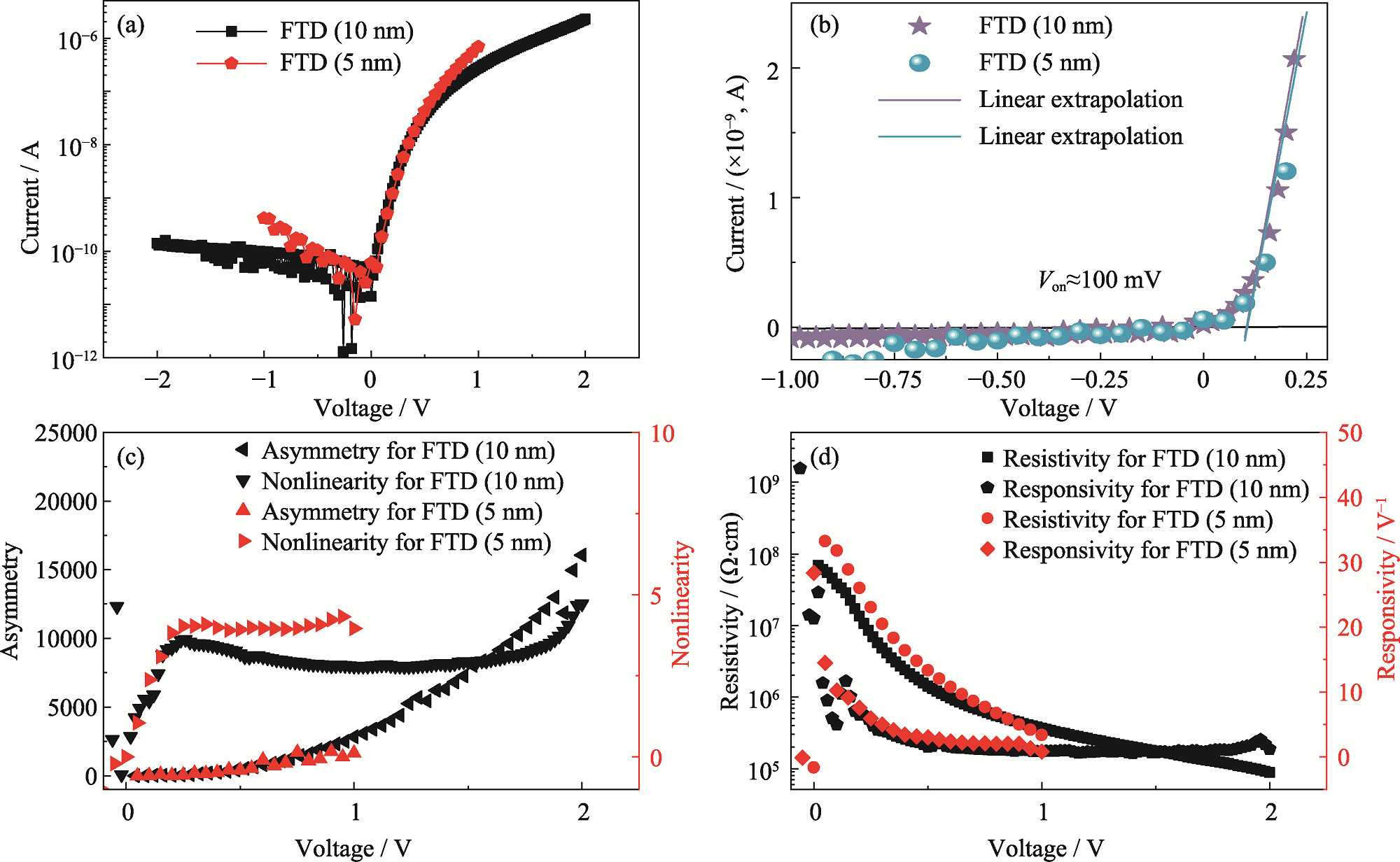
Fig. 5 Rectification performance of FTD (10 nm) and FTD (5 nm) (a) I-V characteristics from experiments of FTD (10 nm) and FTD (5 nm); (b) I-V characteristics of FTD (10 nm) and FTD (5 nm) on a linear scale with Von values being obtained by linear extrapolation; (c) Asymmetry and nonlinearity and (d) responsivity and resistivity of the TiN/ZnO/Pt FTD (10 nm) and FTD (5 nm)
| Structure | fAsy | Von/V | fRes (@0 V)/V-1 | Resistivity/(Ω·cm) |
|---|---|---|---|---|
| Nb/Nb2O3/Pt[ | 1500 | 0.15 | 10 | 8.3×10⁸ (120×120π μm2) |
| Ni/NiO/ZnO/Cr[ | 16 | 0.25 | <5 | 9.5×10⁵ (20×20 μm2) |
| Ti/TiO2/Gr[ | 320 | ~0.8 | 12 | 2.9×10⁴ (140 μm2) |
| Ti/ZnO/Pt[ | <2 | — | 0.125 | 1.125×10⁶ (0.09 mm2) |
| Co/Co3O4/TiO2/Ti[ | 2 | — | 2.2 | 5.8 (0.17 μm2) |
| Pt/Al2O3/Al[ | 107 | 1.4 | <5 | 8.3×10¹² (100 μm2) |
| Pt/ZnO/Al2O3/Al[ | 227 | ~0.5 | 13 | 3000-5000 (10×10 μm2) |
| Cr/TiO2/ZnO/Cr[ | 5.6 | — | 0.28 | 1300 (104 μm2) |
| FTD (10 nm) (This work) | 1.6×10⁴ | 0.1 | 25.3 | 8.8×10⁴ (0.02×500 μm2) |
| FTD (5 nm) (This work) | 1.6×10³ | 0.1 | 28.3 | 8.8×10⁴ (0.02×500 μm2) |
Table 1 Comparison of rectification performance among different tunneling diodes
| Structure | fAsy | Von/V | fRes (@0 V)/V-1 | Resistivity/(Ω·cm) |
|---|---|---|---|---|
| Nb/Nb2O3/Pt[ | 1500 | 0.15 | 10 | 8.3×10⁸ (120×120π μm2) |
| Ni/NiO/ZnO/Cr[ | 16 | 0.25 | <5 | 9.5×10⁵ (20×20 μm2) |
| Ti/TiO2/Gr[ | 320 | ~0.8 | 12 | 2.9×10⁴ (140 μm2) |
| Ti/ZnO/Pt[ | <2 | — | 0.125 | 1.125×10⁶ (0.09 mm2) |
| Co/Co3O4/TiO2/Ti[ | 2 | — | 2.2 | 5.8 (0.17 μm2) |
| Pt/Al2O3/Al[ | 107 | 1.4 | <5 | 8.3×10¹² (100 μm2) |
| Pt/ZnO/Al2O3/Al[ | 227 | ~0.5 | 13 | 3000-5000 (10×10 μm2) |
| Cr/TiO2/ZnO/Cr[ | 5.6 | — | 0.28 | 1300 (104 μm2) |
| FTD (10 nm) (This work) | 1.6×10⁴ | 0.1 | 25.3 | 8.8×10⁴ (0.02×500 μm2) |
| FTD (5 nm) (This work) | 1.6×10³ | 0.1 | 28.3 | 8.8×10⁴ (0.02×500 μm2) |
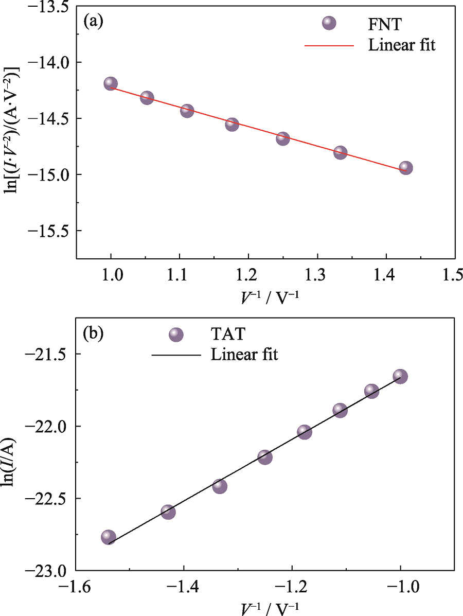
Fig. 6 Fitting of tunneling mechanism for FTD (5 nm) (a) ln(I/V2) vs. V-1 plots with FNT fitting under positive voltage; (b) lnI vs. V-1 plots with TAT fitting under negative voltage
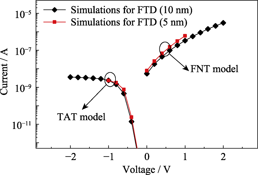
Fig. 7 I-V curves obtained from TCAD simulations for TiN/ZnO/Pt FTDs with tunneling distances of 10 and 5 nm, analyzed using the FNT model under positive bias and the TAT model under negative bias
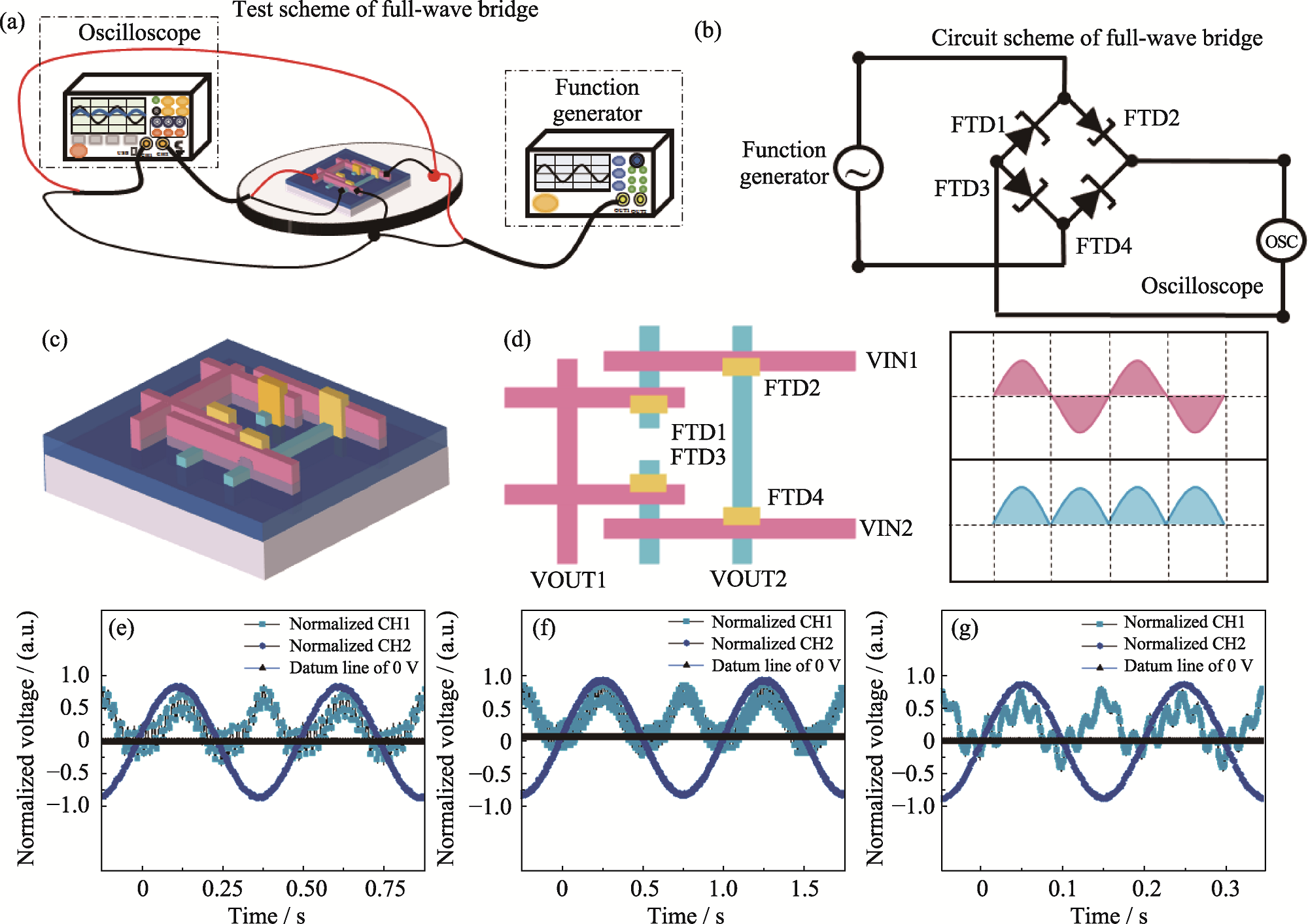
Fig. 8 Scheme and experiment for full-wave rectifier bridge (a) Test scheme for full-wave rectifier bridge; (b) Circuit scheme for full-wave rectifier bridge; (c) Structure schematic of full-wave rectifier bridge; (d) Layout diagram of full wave rectifier circuit (left) and corresponding rectification result (right); (e-g) Normalized full-wave rectification results of full-wave rectifier based on the TiN/ZnO/Pt FTDs with Vpp=1.5 V at frequencies of 1 (e), 2 (f) and 5 Hz (g), respectively
| Parameter | Description | Unit | Value |
|---|---|---|---|
| TOX | Thickness of tunneling layer | Å | 100 |
| IF | Forward Fowler-Nordheim current coefficient | A/V2 | 5×10-16 |
| IR | Reverse Fowler-Nordheim current coefficient | A/V2 | 1×10-16 |
| EF | Forward critical electric field | V/cm | 2×10⁶ |
| ER | Reverse critical electric field | V/cm | 2×10⁸ |
| L | Diode length | m | 2×10⁻⁸ |
| W | Diode width | m | 5×10⁻⁴ |
Table 2 Parameters of the ideal physical model of FTD
| Parameter | Description | Unit | Value |
|---|---|---|---|
| TOX | Thickness of tunneling layer | Å | 100 |
| IF | Forward Fowler-Nordheim current coefficient | A/V2 | 5×10-16 |
| IR | Reverse Fowler-Nordheim current coefficient | A/V2 | 1×10-16 |
| EF | Forward critical electric field | V/cm | 2×10⁶ |
| ER | Reverse critical electric field | V/cm | 2×10⁸ |
| L | Diode length | m | 2×10⁻⁸ |
| W | Diode width | m | 5×10⁻⁴ |
Fig. 9 SPICE simulations for the full-wave rectifier bridge based FTDs with a frequency of 100 GHz and Vpp=2 V
| [1] |
KHAN A A, JAYASWAL G, GAHAFFAR F A, et al. Metal- insulator-metal diodes with sub-nanometre surface roughness for energy-harvesting applications. Microelectron. Eng., 2017, 181: 34.
DOI URL |
| [2] |
DRAGOMAN M, ALDRIGO M. Graphene rectenna for efficient energy harvesting at terahertz frequencies. Appl. Phys. Lett., 2016, 109(11): 113105.
DOI URL |
| [3] |
OLLER D, OSGOOD R, XU J, et al. Optical rectification in a reconfigurable resistive switching filament. Appl. Phys. Lett., 2019, 115(4): 043101.
DOI URL |
| [4] |
WEERAKKODY A, BELKADI A, MODDEL G. Nonstoichiometric nanolayered Ni/NiO/Al2O3/CrAu metal-insulator-metal infrared rectenna. ACS Appl. Nano Mater., 2021, 4(3): 2470.
DOI URL |
| [5] |
BELKADI A, WEERAKKODY A, MODDEL G. Demonstration of resonant tunneling effects in metal-double-insulator-metal (MI(2)M) diodes. Nat. Commun., 2021, 12: 2925.
DOI |
| [6] |
SHAYGAN M, WANG Z, ELSAYED M S, et al. High performance metal-insulator-graphene diodes for radio frequency power detection application. Nanoscale, 2017, 9(33): 11944.
DOI PMID |
| [7] |
SANCHEZ A, DAVIS C F, LIU K C, et al. The MOM tunneling diode: theoretical estimate of its performance at microwave and infrared frequencies. J. Appl. Phys., 1978, 49(10): 5270.
DOI URL |
| [8] |
NISHIDA Y, NISHIGAMI N, DIEBOLD S, et al. Terahertz coherent receiver using a single resonant tunnelling diode. Sci. Rep., 2019, 9: 18125.
DOI PMID |
| [9] |
MITROVIC I Z, ALMALKI S, TEKIN S B, et al. Oxides for rectenna technology. Materials, 2021, 14(18): 5218.
DOI URL |
| [10] |
ALSHEHRI A H, MISTRY K, NGUYEN V H, et al. Quantum- tunneling metal-insulator-metal diodes made by rapid atmospheric pressure chemical vapor deposition. Adv. Funct. Mater., 2018, 29(7): 1805533.
DOI URL |
| [11] |
ANDERSON E C, BOUGHER T L, COLA B A. High performance multiwall carbon nanotube-insulator-metal tunnel diode arrays for optical rectification. Adv. Electron. Mater., 2018, 4(3): 1700446.
DOI URL |
| [12] |
ALSHEHRI A H, SHAHIN A, MISTRY K, et al. Metal- insulator-insulator-metal diodes with responsivities greater than 30 A·W-1 based on nitrogen-doped TiOx and AlOx insulator layers. Adv. Electron. Mater., 2021, 7(11): 2100467.
DOI URL |
| [13] |
ALIMARDANI N, CONLEY J F. Enhancing metal-insulator- insulator-metal tunnel diodes via defect enhanced direct tunneling. Appl. Phys. Lett., 2014, 105(8): 082902.
DOI URL |
| [14] |
SHRIWASTAVA S, TRIPATHI C C. Metal-insulator-metal diodes: a potential high frequency rectifier for rectenna application. J. Electron. Mater., 2019, 48(5): 2635.
DOI |
| [15] | ZHANG X, GRAJAL J, VAZQUEZ-ROY J L, et al. Two- dimensional MoS2-enabled flexible rectenna for Wi-Fi-band wireless energy harvesting. Nature, 2019, 566(7744): 368. |
| [16] |
HOLDEN K E K, QI Y, CONLEY J F. Precision defect engineering of metal/insulator/metal diodes using atomic layer deposition to localize Ni impurities in Al2O3 tunnel barriers. J. Appl. Phys., 2021, 129(14): 144502.
DOI URL |
| [17] |
SINGH A, RATNADURAI R, KUMAR R, et al. Fabrication and current-voltage characteristics of NiOx/ZnO based MIIM tunnel diode. Appl. Surf. Sci., 2015, 334: 197.
DOI URL |
| [18] | RATNADURAI R, KRISHNAN S, STEFANAKOS E, et al. Nanomanufacturability of thin film MIM diodes. AIP Conference Proceedings, 2010, 1313: 403. |
| [19] |
PERIASAMY P, BERRY J J, DAMERON A A, et al. Fabrication and characterization of MIM diodes based on Nb/Nb2O5 via a rapid screening technique. Adv. Mater., 2011, 23(27): 3080.
DOI URL |
| [20] | PERIASAMY P, GUTHREY H L, ABDULAGATOV A I, et al. Metal-insulator-metal diodes: role of the insulator layer on the rectification performance. Adv. Mater., 2013, 25(9): 1301. |
| [21] |
MISTRY K, YAVUZ M, MUSSELMAN K P. Simulated electron affinity tuning in metal-insulator-metal (MIM) diodes. J. Appl. Phys., 2017, 121(18): 184504.
DOI URL |
| [22] |
OZYIGIT D, ULLAH F, GULSARAN A, et al. Manufacturing of quantum-tunneling MIM nanodiodes via rapid atmospheric CVD in terahertz band. Sci. Rep., 2023, 13(1): 20733.
DOI |
| [23] |
WARD D R, HUSER F, PAULY F, et al. Optical rectification and field enhancement in a plasmonic nanogap. Nat. Nanotechnol., 2010, 5(10): 732.
DOI PMID |
| [24] |
LIU Z, ABE S, SHIMIZU M, et al. Enhanced current density and asymmetry of metal-insulator-metal diodes based on self-assembly of Pt nanoparticles. Appl. Phys. Lett., 2023, 122(9): 093502.
DOI URL |
| [25] |
HERNER S B, WEERAKKODY A D, BELKADI A, et al. High performance MIIM diode based on cobalt oxide/titanium oxide. Appl. Phys. Lett., 2017, 110(22): 223901.
DOI URL |
| [26] |
MITROVIC I Z, WEERAKKODY A D, SEDGHI N, et al. Controlled modification of resonant tunneling in metal-insulator- insulator-metal structures. Appl. Phys. Lett., 2018, 112(1): 012902.
DOI URL |
| [27] |
ALSHEHRI A H, ASGARIMOGHADDAM H, DELUMEAU L V, et al. Combinatorial optimization of metal-insulator-insulator-metal (MIIM) diodes with thickness-gradient films via spatial atomic layer deposition. Adv. Electron. Mater., 2024, 10(11): 2400093.
DOI URL |
| [28] |
FENG G, ZHU Q, LIU X, et al. A ferroelectric fin diode for robust non-volatile memory. Nat. Commun., 2024, 15: 513.
DOI PMID |
| [29] |
LIU X, FENG G, FENG X, et al. Ultrahigh rectification ratio in an asymmetric metal/semiconductor/metal nanoscale tunneling junction: implications for high-frequency rectifiers. ACS Appl. Nano Mater., 2023, 6(4): 2491.
DOI URL |
| [30] |
LIU H, ZHANG L, LEBEGUE S, et al. Morphology-electronic effects in ultra-model nanocatalysts under the CO oxidation reaction: the case of ZnO ultrathin films grown on Pt(111). Nanoscale, 2024, 16(43): 20216.
DOI URL |
| [31] |
CHEN T, YU K, HU H, et al. Engineering electron transport layer with ionic liquid for high-performance quantum dot light-emitting diodes. ACS Appl. Nano Mater., 2025, 8(9): 4573.
DOI URL |
| [32] |
SHINDE P, HASE Y, DOIPHODE V, et al. Morphology-dependent ZnO/MoS2 heterostructures for enhanced photoelectrochemical water splitting. ACS Appl. Energ. Mater., 2025, 8(2): 935.
DOI URL |
| [33] |
ALIMARDANI N, KING S W, FRENCH B L, et al. Investigation of the impact of insulator material on the performance of dissimilar electrode metal-insulator-metal diodes. J. Appl. Phys., 2014, 116(2): 024508.
DOI URL |
| [34] |
CONG X, ZHENG Y, HUANG F, et al. Efficiently band-tailored type-Ⅲ van der Waals heterostructure for tunnel diodes and optoelectronic devices. Nano Res., 2022, 15(9): 8442.
DOI |
| [35] |
LEE G H, YU Y J, LEE C, et al. Electron tunneling through atomically flat and ultrathin hexagonal boron nitride. Appl. Phys. Lett., 2011, 99(24): 243114.
DOI URL |
| [36] |
MA Q, ANDERSEN T I, NAIR N L, et al. Tuning ultrafast electron thermalization pathways in a van der Waals heterostructure. Nat. Phys., 2016, 12(5): 455.
DOI |
| [37] |
VU Q A, LEE J H, NGUYEN V L, et al. Tuning carrier tunneling in van der waals heterostructures for ultrahigh detectivity. Nano Lett., 2017, 17(1): 453.
DOI PMID |
| [38] |
TEKIN S B, ALMALKI S, FINCH H, et al. Electron affinity of metal oxide thin films of TiO2, ZnO, and NiO and their applicability in 28.3 THz rectenna devices. J. Appl. Phys., 2023, 134(8): 084503.
DOI URL |
| [39] | FOWLER R H, NORDHEIM L. Electron emission in intense electric fields. Proc. Roy. Soc. A, 1928, 119(791): 173. |
| [40] |
YU S, GUAN X, WONG H S P. Conduction mechanism of TiN/HfOx/Pt resistive switching memory: a trap-assisted-tunneling model. Appl. Phys. Lett., 2011, 99(6): 063507.
DOI URL |
| [41] |
CHANG W J, HOUNG M P, WANG Y H. Electrical properties and modeling of ultrathin impurity-doped silicon dioxides. J. Appl. Phys., 2001, 90(10): 5171.
DOI URL |
| [42] |
TSIARAPAS C, GIRGINOUDI D, DIMITRIADIS E I, et al. Investigation on deep level defects in polycrystalline ZnO thin films. J. Vac. Sci. Technol. B, 2017, 35(3): 031203.
DOI URL |
| [1] | 洪恩柳, 涂欣晨, 李自清, 方晓生. 二维钙钛矿单晶纳米片的漂浮法制备及其光电探测性能[J]. 无机材料学报, 2026, 41(6): 787-794. |
| [2] | 王萌萌, 田力, 张俊敏, 李庆刚, 杨金山, 董绍明. 3D打印制备CNT/SiC-SiO2及其电磁屏蔽性能[J]. 无机材料学报, 2026, 41(6): 831-838. |
| [3] | 李涵涛, 沈强, 罗国强, 王雪飞, 高明, 陈晨. 机械球磨法调控硅基负极材料结构与性能的研究进展[J]. 无机材料学报, 2026, 41(5): 561-572. |
| [4] | 钱新宇, 王无敌, 郭俊尧, 任永春, 董建树, 王庆国, 唐慧丽, 张晨波, 徐晓东, 董永军, 华伟, 徐军. Ho:BaF2晶体在近红外-中红外波段光谱性能分析[J]. 无机材料学报, 2026, 41(5): 595-603. |
| [5] | 朱开煌, 杨世杰, 李欣格, 宋贯卿, 史淦升, 王焱, 任小孟, 陆遥, 徐新宏, 孙静. 基于UiO-66骨架的氧化石墨烯改性金属有机框架凝胶的制备及其对甲苯的高效吸附性能[J]. 无机材料学报, 2026, 41(4): 519-526. |
| [6] | 蒋圣楠, 郑重, 何唯一, 刘涛, 潘秀红, 陈锟, 郭辉, 高攀, 刘春俊, 刘学超. 硼镓共掺氧化锌透明电极的制备及性能优化[J]. 无机材料学报, 2026, 41(4): 479-485. |
| [7] | 徐浩, 顾海涛, 吴鸿辉, 岳晓飞, 林思琪, 金敏. Bi掺杂InSe晶体生长及性能研究[J]. 无机材料学报, 2026, 41(4): 493-499. |
| [8] | 张梦婕, 李智博, 黄瑞楠, 吕向菲, 王伟. 堇青石/硼酸铝晶须/Co0.8FexCe0.2-xCr2O4催化剂的制备及其碳烟过滤-催化燃烧性能[J]. 无机材料学报, 2026, 41(4): 509-518. |
| [9] | 隋金洋, 周大雨, 赵文瑾, 童祎, 王新朋. 工作气压对AlScN薄膜结构和电学性能的影响[J]. 无机材料学报, 2026, 41(4): 486-492. |
| [10] | 程澳芃, 王跃文, 许文涛, 刘全伟, 张海涛, 周有福. 吸附-沉淀自组装结合放电等离子烧结法制备石墨烯增强氧化铝复合陶瓷[J]. 无机材料学报, 2026, 41(4): 536-544. |
| [11] | 李璇, 叶奎材, 冯佳音, 邱家军, 钱文昊, 邢敏. 钛基牙种植体表面改性促进软组织封闭的研究进展[J]. 无机材料学报, 2026, 41(4): 432-444. |
| [12] | 王禹贺, 罗颐秀, 郭会明, 张广珩, 张思岩, 孙鲁超, 王杰民, 王京阳. 高熵稀土氧化物热障涂层材料弹性及热物性的第一性原理研究[J]. 无机材料学报, 2026, 41(4): 445-454. |
| [13] | 李泽熙, 卢文杰, 王朝, 张璐, 李述体, 高芳亮. 基于液态金属镓制备二维氮化镓及其光电性能研究[J]. 无机材料学报, 2026, 41(3): 377-384. |
| [14] | 田洪旺, 罗龙飞, 胡成龙, 闫猛, 庞生洋, 李建, 汤素芳. C/CA表面陶瓷-树脂涂层的简易制备与中温抗氧化性能[J]. 无机材料学报, 2026, 41(3): 401-408. |
| [15] | 曹娟, 吴西士, 刘泽华, 裴兵兵, 韩建燊, 刘欢, 杨亦天, 吴海波, 黄政仁. 晶粒尺寸对常压固相烧结SiC陶瓷断裂强度Weibull分布的影响[J]. 无机材料学报, 2026, 41(2): 217-224. |
| 阅读次数 | ||||||
|
全文 |
|
|||||
|
摘要 |
|
|||||