无机材料学报 ›› 2025, Vol. 40 ›› Issue (9): 1022-1028.DOI: 10.15541/jim20250022 CSTR: 32189.14.jim20250022
所属专题: 【结构材料】热障与环境障涂层(202512); 【信息功能】透明与闪烁陶瓷(202512)
王亮君1( ), 欧阳玉昭1, 赵俊亮2, 杨长1()
收稿日期:2025-01-15
修回日期:2025-02-13
出版日期:2025-09-20
网络出版日期:2025-03-19
通讯作者:
杨长, 教授. E-mail: cyang@phy.ecnu.edu.cn作者简介:王亮君(1998-), 男, 博士研究生. E-mail: 1134420548@qq.com
基金资助:
WANG Liangjun1(), OUYANG Yuzhao1, ZHAO Junliang2, YANG Chang1()
Received:2025-01-15
Revised:2025-02-13
Published:2025-09-20
Online:2025-03-19
Contact:
YANG Chang, professor. E-mail: cyang@phy.ecnu.edu.cnAbout author:WANG Liangjun (1998-), male, PhD candidate. E-mail: 1134420548@qq.com
Supported by:摘要:
在光电子器件领域, 具有可控电学参数的p型透明半导体材料具有重要的应用价值。但以CuI为代表的该类材料在制备工艺与掺杂调控方面仍存在显著技术瓶颈。本研究通过锰阳离子掺杂, 成功制备出具有可调电学特性的新型p型透明半导体材料, 为透明电子学发展提供了新思路。采用反应磁控溅射技术制备的Cu1-xMnxI固溶体薄膜展现出独特的性能优势。首先, 该材料可以在室温条件下制备, 并保持优异的可见光透明性。其次, 随着锰掺杂量(x)的增加, 薄膜晶粒尺寸逐渐减小, 并且出现明显的晶粒团聚现象。通过X射线光电子能谱分析, 揭示了薄膜中锰离子以Mn2+和Mn3+混合价态存在。电学性能表征显示, 薄膜电阻率可在0.017~2.5 Ω·cm区间实现两个数量级的可控调节, 同时空穴载流子浓度稳定维持在1018~1019 cm-3较高数量级。与传统n型半导体掺杂规律不同, 引入高价态锰离子未显著影响材料的p型导电特性, 这可能源于锰取代亚铜离子后形成的非完全离域电子态。本研究表明CuI半导体的空穴导电特性不易受高价锰离子掺杂的影响, 有望在保持良好p型导电性的情况下在较大范围内实现材料组分的宽域调控, 为开发CuI基多功能透明电子器件提供了重要材料基础。
中图分类号:
王亮君, 欧阳玉昭, 赵俊亮, 杨长. Cu-Mn-I固溶体薄膜制备及其p型透明导电性质调控[J]. 无机材料学报, 2025, 40(9): 1022-1028.
WANG Liangjun, OUYANG Yuzhao, ZHAO Junliang, YANG Chang. Cu-Mn-I Solid Solution Thin Films: Preparation and Control of p-type Transparent Conductive Properties[J]. Journal of Inorganic Materials, 2025, 40(9): 1022-1028.
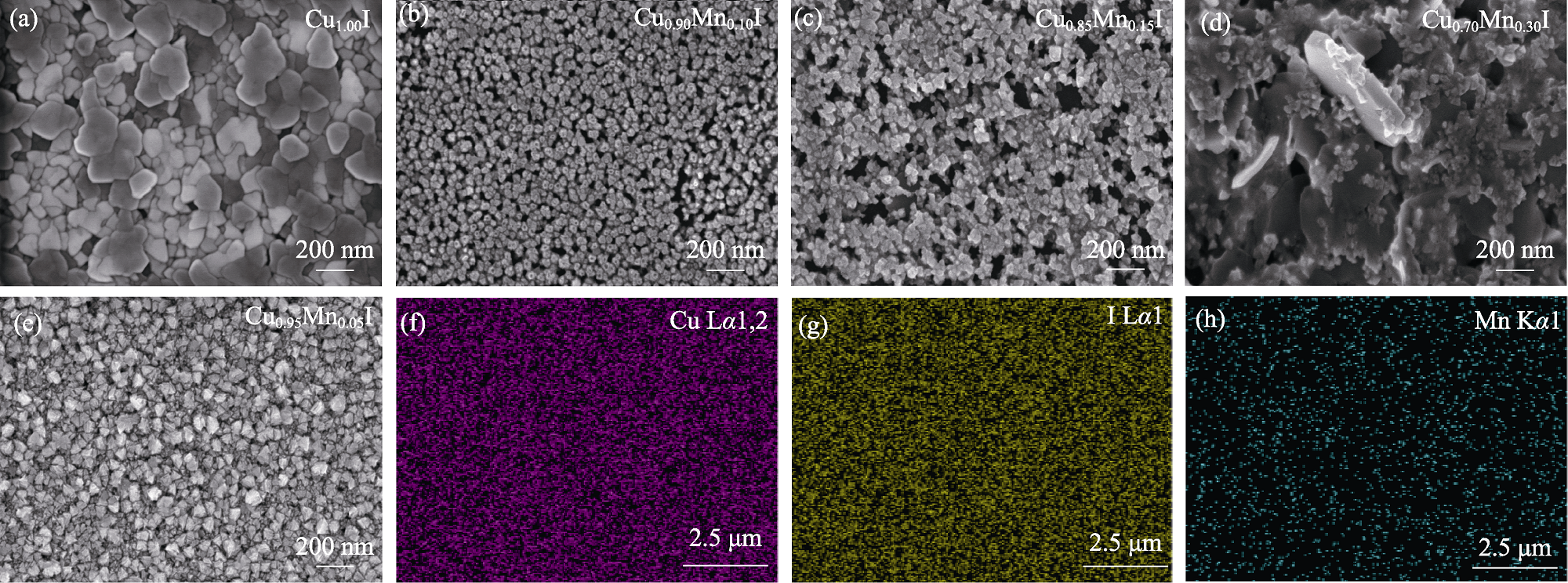
图1 Cu1-xMnxI薄膜的SEM照片(a~e)和Cu0.95Mn0.05I薄膜的元素面分布图(f~h)
Fig. 1 SEM images of Cu1-xMnxI thin films (a-e) and elemental distribution mappings of Cu0.95Mn0.05I thin films (f-h)
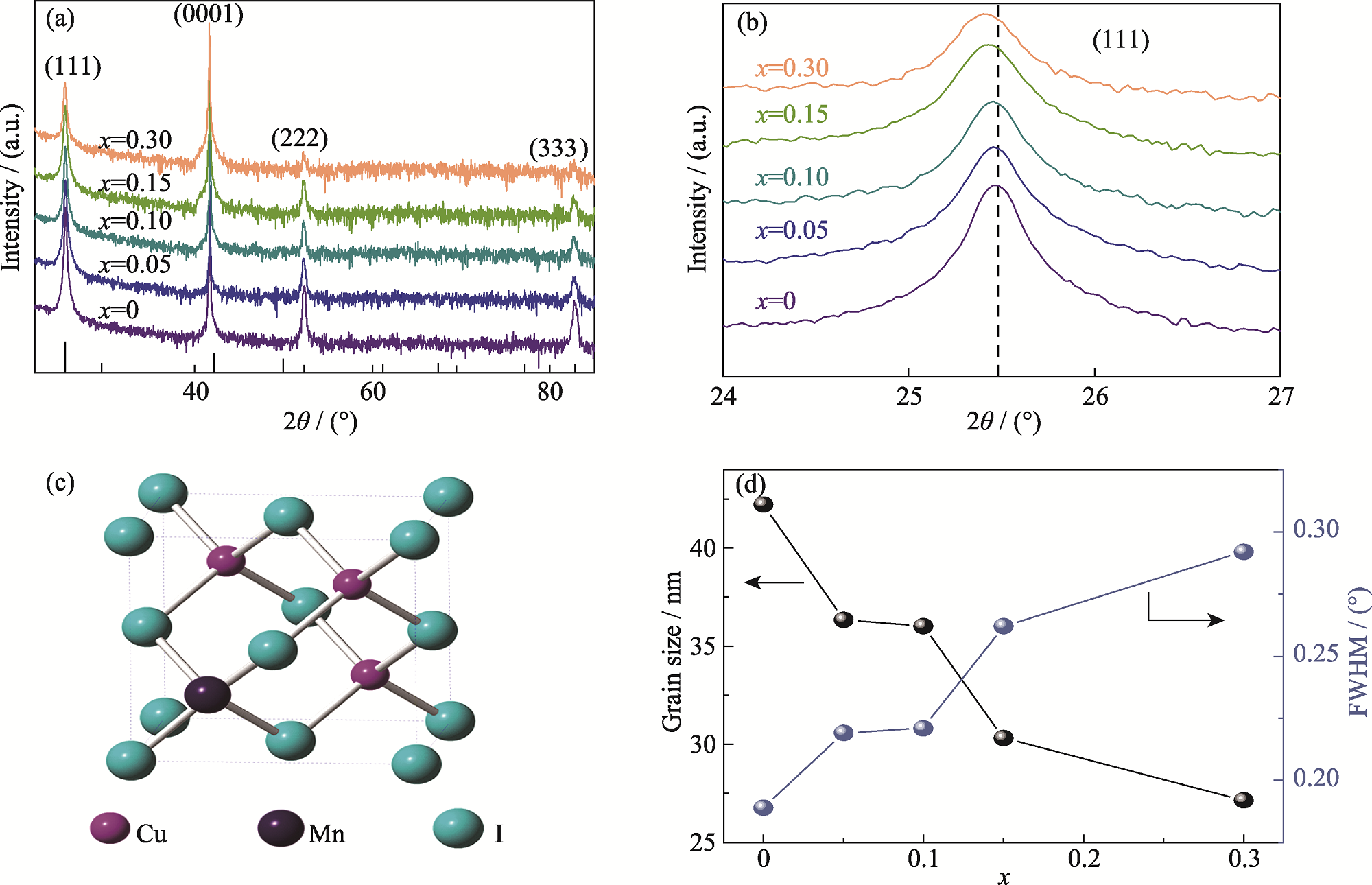
图2 Cu1-xMnxI薄膜晶体结构分析
Fig. 2 Crystal structure analyses of Cu1-xMnxI thin films (a) XRD patterns; (b) Localized magnified patterns of diffraction peak (111); (c) Schematic diagram of manganese ions replacing copper ions; (d) Dependence of grain size and FWHM on x
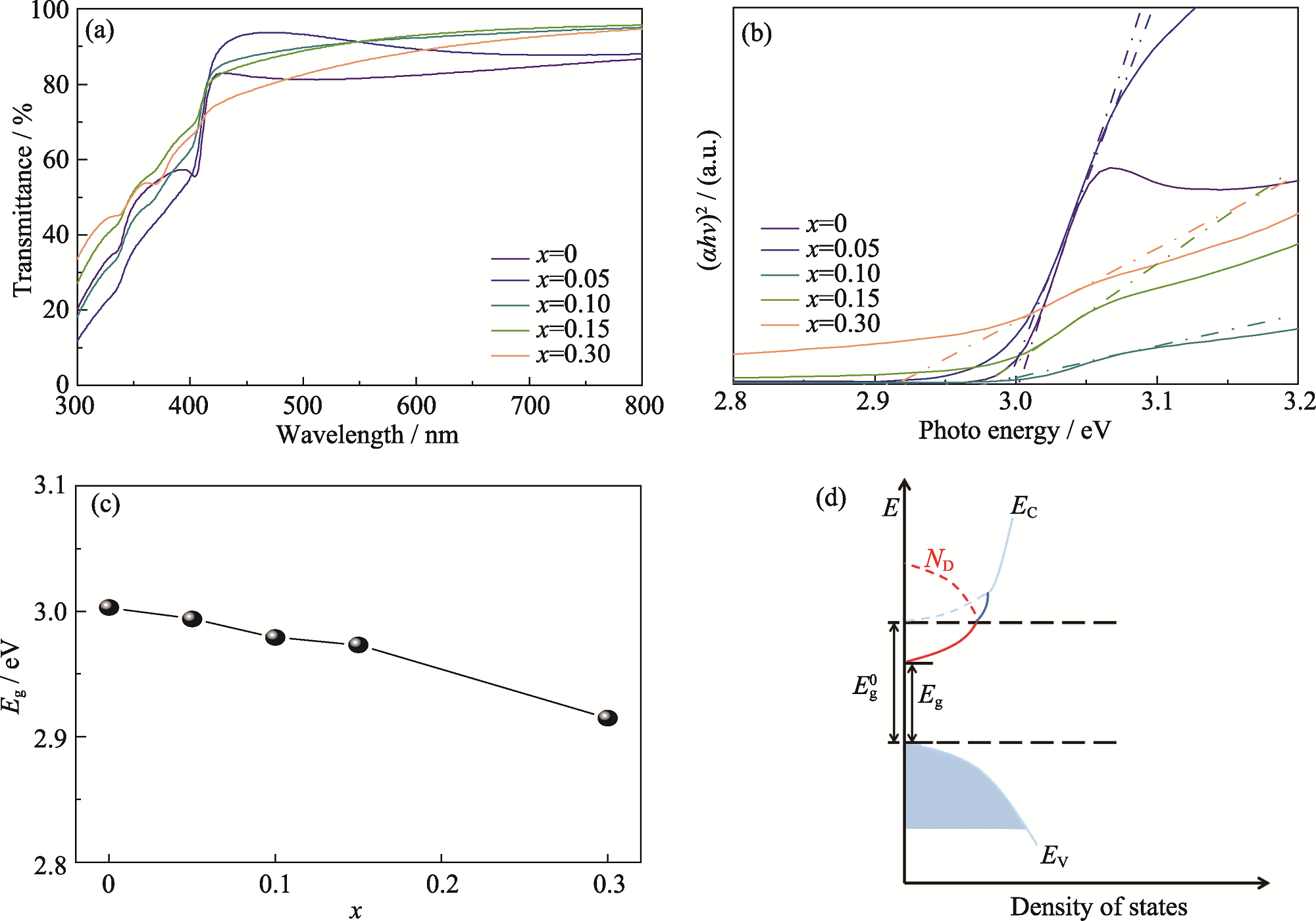
图3 Cu1-xMnxI薄膜光学带隙分析
Fig. 3 Analyses of optical bandgap of Cu1-xMnxI thin films (a) UV-Vis transmission spectra; (b) Tauc plots; (c) Dependence of Eg on x; (d) Schematic diagram of the influence of donor energy levels on Eg. Colorful figures are available on website
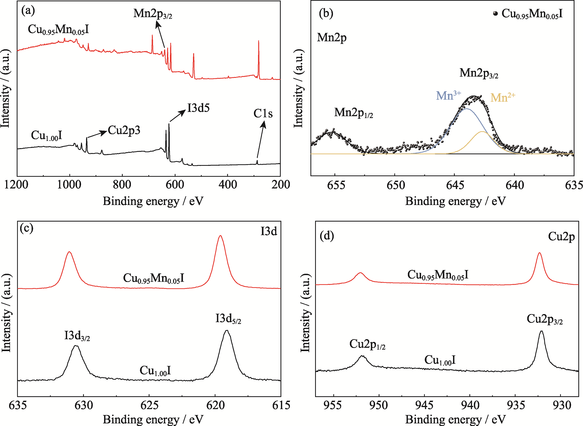
图4 Cu1.00I和Cu0.95Mn0.05I薄膜的XPS图谱
Fig. 4 XPS spectra of Cu1.00I and Cu0.95Mn0.05I thin films (a) XPS survey spectra; (b) High-resolution Mn2p XPS spectra of Cu0.95Mn0.05I films; (c, d) High-resolution I3d (c) and Cu2p (d) XPS spectra of Cu1.00I and Cu0.95Mn0.05I thin films
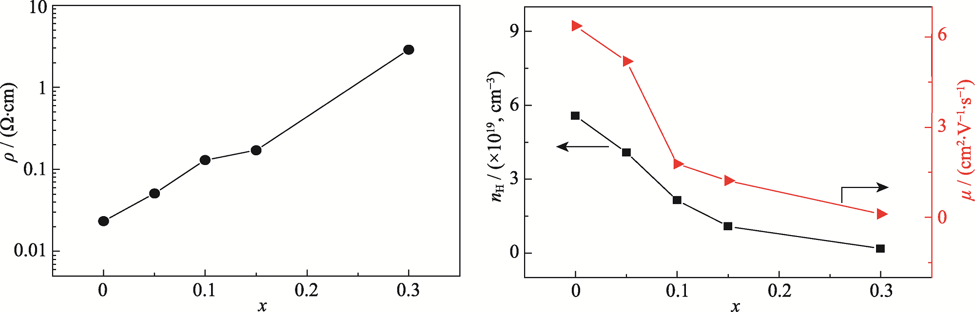
图5 Cu1-xMnxI薄膜电阻率、载流子浓度以及迁移率与x之间的关系
Fig. 5 Dependence of x on resistivity, carrier density, and mobility in Cu1-xMnxI thin films
| [1] | LIU A, ZHU H H, KIM M G, et al. Engineering copper iodide (CuI) for multifunctional p-type transparent semiconductors and conductors. Advanced Science, 2021, 8(14): 2100546. |
| [2] | THOMAS G. Invisible circuits. Nature, 1997, 389(6654): 907. |
| [3] | KAWAZOE H, YASUKAWA M, HYODO H, et al. P-type electrical conduction in transparent thin films of CuAlO2. Nature, 1997, 389(6654): 939. |
| [4] | UEDA K, HASE T, YANAGI H, et al. Epitaxial growth of transparent p-type conducting CuGaO2 thin films on sapphire (001) substrates by pulsed laser deposition. Journal of Applied Physics, 2001, 89(3): 1790. |
| [5] | YANAGI H, HASE T, IBUKI S, et al. Bipolarity in electrical conduction of transparent oxide semiconductor CuInO2 with delafossite structure. Applied Physics Letters, 2001, 78(11): 1583. |
| [6] | KUDO A, YANAGI H, HOSONO H, et al. SrCu2O2: a p-type conductive oxide with wide band gap. Applied Physics Letters, 1998, 73(2): 220. |
| [7] | RAGHUPATHY R K M, KÜHNE T D, FELSER C, et al. Rational design of transparent p-type conducting non-oxide materials from high-throughput calculations. Journal of Materials Chemistry C, 2018, 6(3): 541. |
| [8] | YANG C, KNEIß M, LORENZ M, et al. Room-temperature synthesized copper iodide thin film as degenerate p-type transparent conductor with a boosted figure of merit. Proceedings of the National Academy of Sciences, 2016, 113(46): 12929. |
| [9] | GENG F J, WANG L J, STRALKA, et al. (111)-oriented growth and acceptor doping of transparent conductive CuI:S thin films by spin coating and radio frequency-sputtering. Advanced Engineering Materials, 2023, 25(11): 2201666. |
| [10] | YANG J L, JIANG X L, RUAN S Y, et al. Highly weak-light sensitive and dual-band switchable photodetector based on CuI/Si unilateral heterojunction. Journal of Inorganic Materials, 2024, 39(9): 1063. |
| [11] | GRUNDMANN M, SCHEIN F L, LORENZ M, et al. Cuprous iodide - a p-type transparent semiconductor: history and novel applications. Physica Status Solidi A, 2013, 210(9): 1671. |
| [12] | GRUNDMANN M. Karl Bädeker (1877-1914) and the discovery of transparent conductive materials. Physica Status Solidi A, 2015, 212(7): 1409. |
| [13] | CHEN D, WANG Y, LIN Z, et al. Growth strategy and physical properties of the high mobility p-type CuI crystal. Crystal Growth & Design, 2010, 10(5): 2057. |
| [14] | JUN T, KIM J, SASASE M, et al. Material design of p-type transparent amorphous semiconductor, Cu-Sn-I. Advance Materials, 2018, 30(12): 1706573. |
| [15] | YANG C, SOUCHAY D, KNEIß M, et al. Transparent flexible thermoelectric material based on non-toxic earth-abundant p-type copper iodide thin film. Nature Communications, 2017, 8: 16076. |
| [16] | ZENG G X, DOU W, GAN X M, et al. Low-voltage solution-processed NaxCu1-xI thin-film transistors for mimicking synaptic plasticity. Applied Physical Letters, 2024, 124(12): 123508. |
| [17] | JIANG G G, DOU W, GAN X M, et al. Low-voltage solution- processed p-type Mg-doped CuI thin film transistors with NAND logic function. Applied Physical Letters, 2023, 122(21): 213501. |
| [18] | GHAZAL N, MADKOUR M, NAZEER A A, et al. Electrochemical capacitive performance of thermally evaporated Al-doped CuI thin films. RSC Advance, 2021, 11(62): 39262. |
| [19] | MIRZA A S, VISHAL B, DALLY P, et al. Cs-doped and Cs-S co-doped CuI p-type transparent semiconductors with enhanced conductivity. Advanced Functional Materials, 2024, 34(30): 2316144. |
| [20] | MUDE N N, BUKKE R N, JIANG J. Transparent, p-channel CuISn thin-film transistor with field effect mobility of 45 cm2·V-1·s-1 and excellent bias stability. Advanced Materials Technologies, 2022, 7(8): 2101434. |
| [21] | TAREY R D, RAJU T A. A method for the deposition of transparent conducting thin films of tin oxide. Thin Solid Films, 1985, 128(3/4): 181. |
| [22] | LIU A, ZHU H H, PARK W T, et al. Room-temperature solution-synthesized p-type copper(I) iodide semiconductors for transparent thin-film transistors and complementary electronics. Advanced Materials, 2018, 30(34): 1802379. |
| [23] | STRELCHUNK V, KOLOMYS O, RARATA S, et al. Raman submicron spatial mapping of individual Mn-doped ZnO nanorods. Nano Epress, 2017, 12: 1. |
| [24] | ZI M, LI J, ZHANG Z C, et al. Effect of deposition temperature on transparent conductive properties of γ-CuI film prepared by vacuum thermal evaporation. Physica Status Solidi A, 2015, 212(7): 1466. |
| [25] | SUNG S Y, KIM S Y, JO K M, et al. Fabrication of p-channel thin-film transistors using CuO active layers deposited at low temperature. Applied Physical Letters, 2010, 97(22): 222109. |
| [26] | KYKYNESHI R, MCINTYRE D H, TATE J, et al. Electrical and optical properties of epitaxial transparent conductive BaCuTeF thin films deposited by pulsed laser deposition. Solid State Sciences, 2008, 10(7): 921. |
| [27] | ZAKUTAYEV A, MCINTYRE D H, SCHNEIDER G, et al. Tunable properties of wide-band gap p-type BaCu(Ch1-xChx′)F (Ch=S, Se, Te) thin-film solid solutions. Thin Solid Films, 2010, 518(19): 5494. |
| [28] | YANG C, KNEIß M, SCHEIN F L, et al. Room-temperature domain-epitaxy of copper iodide thin films for transparent CuI/ZnO heterojunctions with high rectification ratios larger than 109. Scientific Reports, 2016, 6: 21937. |
| [29] | YANG C, ROSE E, YU W L, et al. Controllable growth of copper iodide for high-mobility thin films and self-assembled microcrystals. ACS Applied Electronic Materials, 2020, 2(11): 3627. |
| [1] | 王萌萌, 田力, 张俊敏, 李庆刚, 杨金山, 董绍明. 3D打印制备CNT/SiC-SiO2及其电磁屏蔽性能[J]. 无机材料学报, 2026, 41(6): 831-838. |
| [2] | 洪恩柳, 涂欣晨, 李自清, 方晓生. 二维钙钛矿单晶纳米片的漂浮法制备及其光电探测性能[J]. 无机材料学报, 2026, 41(6): 787-794. |
| [3] | 李涵涛, 沈强, 罗国强, 王雪飞, 高明, 陈晨. 机械球磨法调控硅基负极材料结构与性能的研究进展[J]. 无机材料学报, 2026, 41(5): 561-572. |
| [4] | 钱新宇, 王无敌, 郭俊尧, 任永春, 董建树, 王庆国, 唐慧丽, 张晨波, 徐晓东, 董永军, 华伟, 徐军. Ho:BaF2晶体在近红外-中红外波段光谱性能分析[J]. 无机材料学报, 2026, 41(5): 595-603. |
| [5] | 朱开煌, 杨世杰, 李欣格, 宋贯卿, 史淦升, 王焱, 任小孟, 陆遥, 徐新宏, 孙静. 基于UiO-66骨架的氧化石墨烯改性金属有机框架凝胶的制备及其对甲苯的高效吸附性能[J]. 无机材料学报, 2026, 41(4): 519-526. |
| [6] | 蒋圣楠, 郑重, 何唯一, 刘涛, 潘秀红, 陈锟, 郭辉, 高攀, 刘春俊, 刘学超. 硼镓共掺氧化锌透明电极的制备及性能优化[J]. 无机材料学报, 2026, 41(4): 479-485. |
| [7] | 徐浩, 顾海涛, 吴鸿辉, 岳晓飞, 林思琪, 金敏. Bi掺杂InSe晶体生长及性能研究[J]. 无机材料学报, 2026, 41(4): 493-499. |
| [8] | 张梦婕, 李智博, 黄瑞楠, 吕向菲, 王伟. 堇青石/硼酸铝晶须/Co0.8FexCe0.2-xCr2O4催化剂的制备及其碳烟过滤-催化燃烧性能[J]. 无机材料学报, 2026, 41(4): 509-518. |
| [9] | 隋金洋, 周大雨, 赵文瑾, 童祎, 王新朋. 工作气压对AlScN薄膜结构和电学性能的影响[J]. 无机材料学报, 2026, 41(4): 486-492. |
| [10] | 程澳芃, 王跃文, 许文涛, 刘全伟, 张海涛, 周有福. 吸附-沉淀自组装结合放电等离子烧结法制备石墨烯增强氧化铝复合陶瓷[J]. 无机材料学报, 2026, 41(4): 536-544. |
| [11] | 李璇, 叶奎材, 冯佳音, 邱家军, 钱文昊, 邢敏. 钛基牙种植体表面改性促进软组织封闭的研究进展[J]. 无机材料学报, 2026, 41(4): 432-444. |
| [12] | 王禹贺, 罗颐秀, 郭会明, 张广珩, 张思岩, 孙鲁超, 王杰民, 王京阳. 高熵稀土氧化物热障涂层材料弹性及热物性的第一性原理研究[J]. 无机材料学报, 2026, 41(4): 445-454. |
| [13] | 李泽熙, 卢文杰, 王朝, 张璐, 李述体, 高芳亮. 基于液态金属镓制备二维氮化镓及其光电性能研究[J]. 无机材料学报, 2026, 41(3): 377-384. |
| [14] | 田洪旺, 罗龙飞, 胡成龙, 闫猛, 庞生洋, 李建, 汤素芳. C/CA表面陶瓷-树脂涂层的简易制备与中温抗氧化性能[J]. 无机材料学报, 2026, 41(3): 401-408. |
| [15] | 邓恒杨, 秦翠洁, 郝胜兰, 冯光迪, 朱秋香, 田博博, 褚君浩, 段纯刚. 基于金属-半导体-金属鳍式隧穿二极管的高频整流桥电路[J]. 无机材料学报, 2026, 41(2): 253-261. |
| 阅读次数 | ||||||
|
全文 |
|
|||||
|
摘要 |
|
|||||