
Journal of Inorganic Materials ›› 2026, Vol. 41 ›› Issue (2): 253-261.DOI: 10.15541/jim20250076
• RESEARCH LETTER • Previous Articles Next Articles
DENG Hengyang1( ), QIN Cuijie1, HAO Shenglan1, FENG Guangdi1,2, ZHU Qiuxiang1(), TIAN Bobo1,2(), CHU Junhao1, DUAN Chungang1,3
Received:2025-02-22
Revised:2025-03-14
Published:2026-02-20
Online:2025-05-09
Contact:
ZHU Qiuxiang, associate professor. E-mail: qxzhu@clpm.ecnu.edu.cn;About author:DENG Hengyang (1999-), male, Master candidate. E-mail: 51254700083@stu.ecnu.edu.cn
Supported by:CLC Number:
DENG Hengyang, QIN Cuijie, HAO Shenglan, FENG Guangdi, ZHU Qiuxiang, TIAN Bobo, CHU Junhao, DUAN Chungang. A Rectifier Bridge Circuit Based on Metal-semiconductor-metal Fin Tunneling Diode for High-frequency Application[J]. Journal of Inorganic Materials, 2026, 41(2): 253-261.
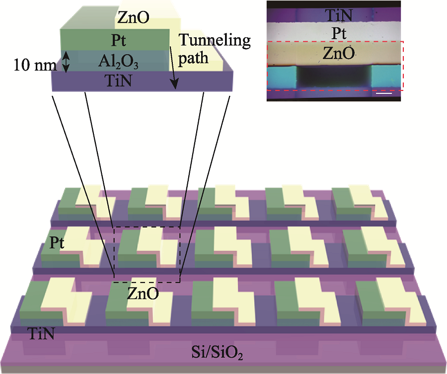
Fig. 1 Schematic diagram of line array constituted by TiN/ZnO/Pt FTDs fabricated on a Si/SiO2 substrate, along with cross-sectional view of a single device Upper right inset shows an optical image of an individual device from the top view (scale: 100 μm)
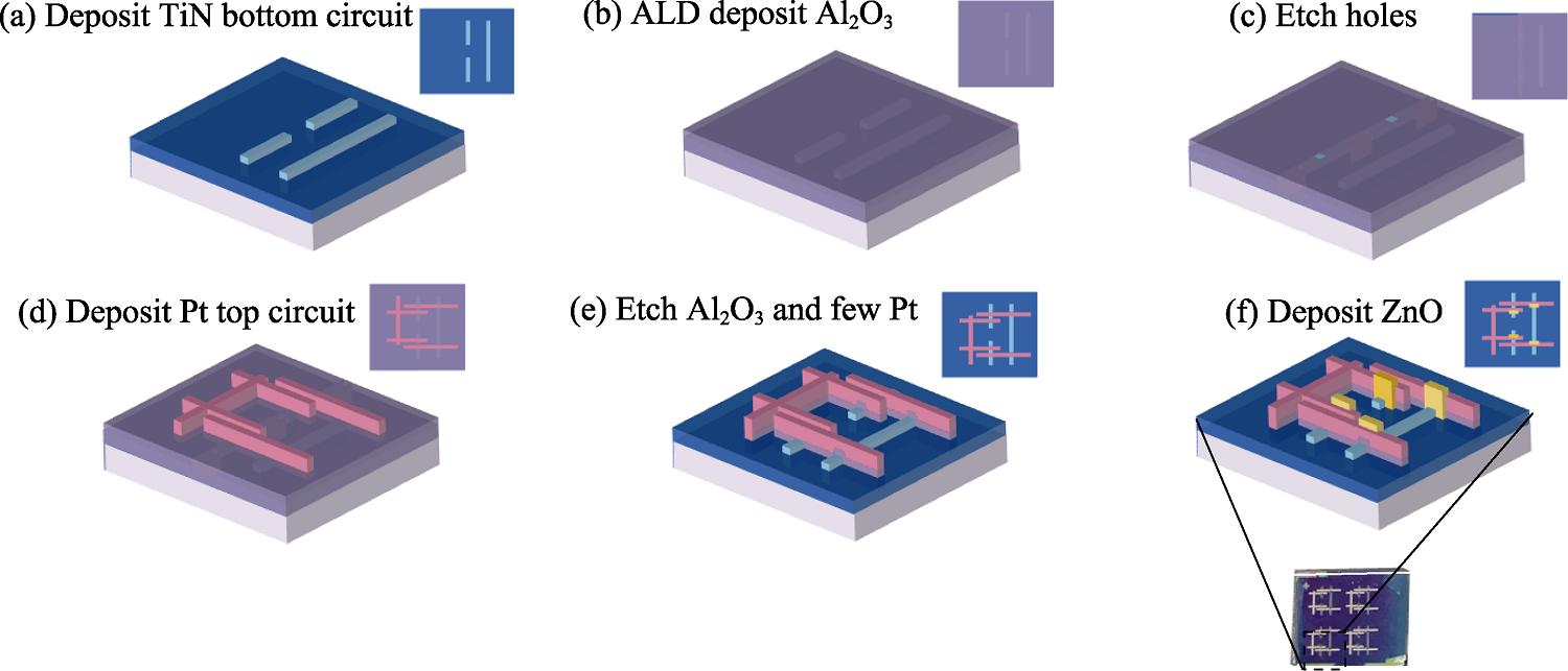
Fig. 2 Fabrication process of the rectifier bridge (a) Deposit TiN bottom circuit; (b) ALD (Atomic layer deposition) deposit Al2O3; (c) Etch holes; (d) Deposit Pt top circuit; (e) Etch Al2O3 and few Pt; (f) Deposit ZnO
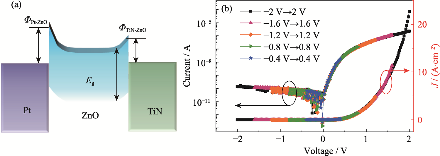
Fig. 3 Energy band alignments and electrical characteristics (a) Energy band alignments of ZnO and electrodes (Pt and TiN) after contact; (b) I-V and J-V characteristics of the TiN/ZnO/Pt FTD device across various bias voltage ranges, where the bias is applied to the bottom electrode (TiN) and the top electrode (Pt) remains grounded
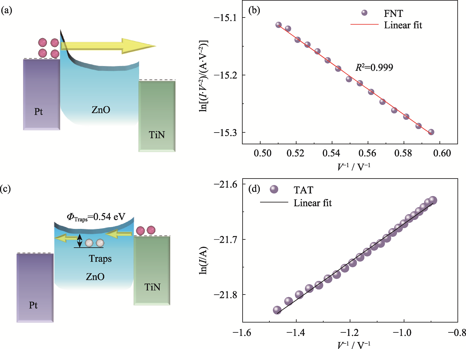
Fig. 4 Energy band alignments and fitting of tunneling mechanism of the FTD (a) Energy band alignments of the FTD and (b) ln(I/V2) vs. V-1 plots with FNT fitting under positive voltage; (c) Energy band alignments of the FTD and (d) lnI vs. V-1 plots with TAT fitting under negative voltage
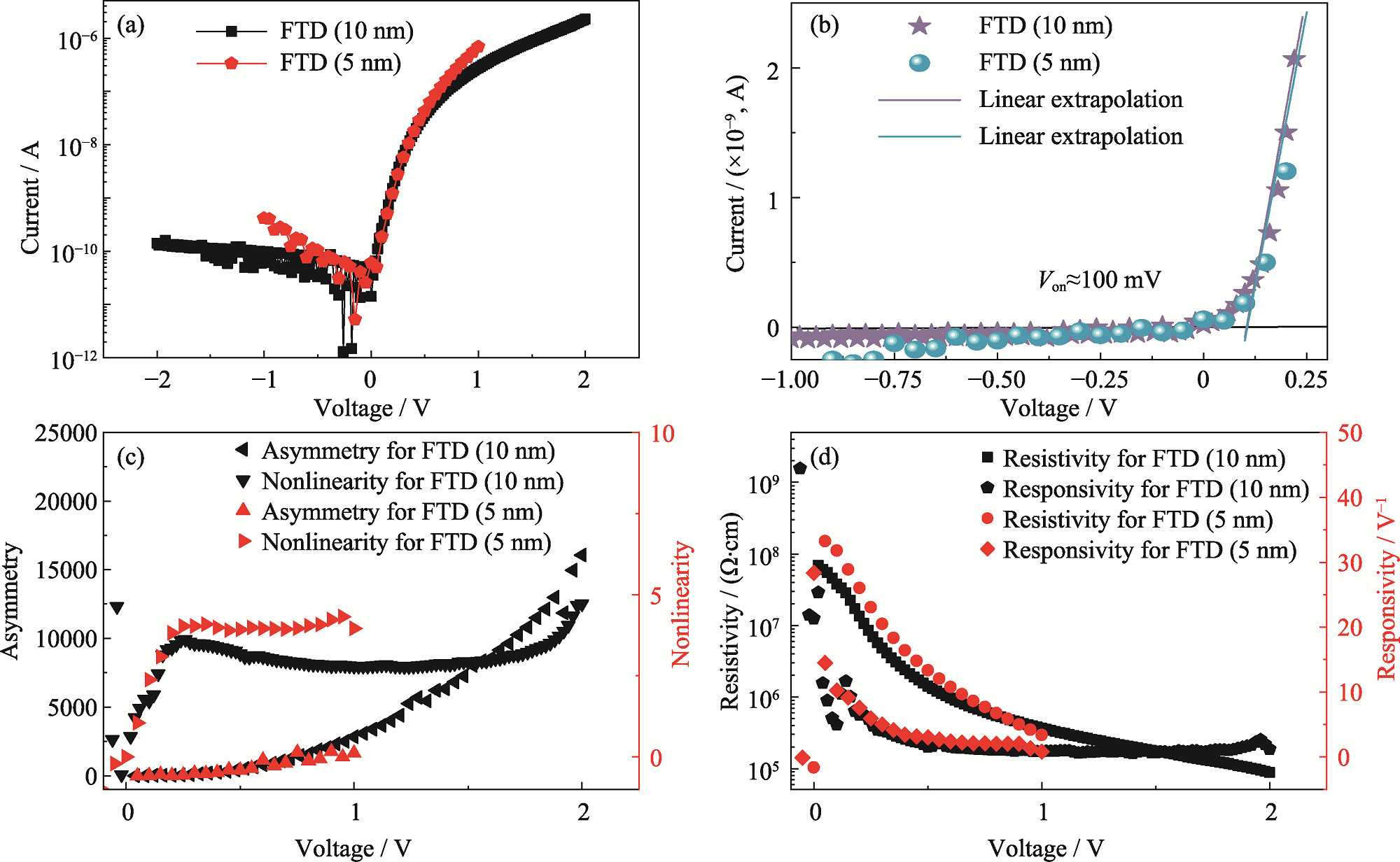
Fig. 5 Rectification performance of FTD (10 nm) and FTD (5 nm) (a) I-V characteristics from experiments of FTD (10 nm) and FTD (5 nm); (b) I-V characteristics of FTD (10 nm) and FTD (5 nm) on a linear scale with Von values being obtained by linear extrapolation; (c) Asymmetry and nonlinearity and (d) responsivity and resistivity of the TiN/ZnO/Pt FTD (10 nm) and FTD (5 nm)
| Structure | fAsy | Von/V | fRes (@0 V)/V-1 | Resistivity/(Ω·cm) |
|---|---|---|---|---|
| Nb/Nb2O3/Pt[ | 1500 | 0.15 | 10 | 8.3×10⁸ (120×120π μm2) |
| Ni/NiO/ZnO/Cr[ | 16 | 0.25 | <5 | 9.5×10⁵ (20×20 μm2) |
| Ti/TiO2/Gr[ | 320 | ~0.8 | 12 | 2.9×10⁴ (140 μm2) |
| Ti/ZnO/Pt[ | <2 | — | 0.125 | 1.125×10⁶ (0.09 mm2) |
| Co/Co3O4/TiO2/Ti[ | 2 | — | 2.2 | 5.8 (0.17 μm2) |
| Pt/Al2O3/Al[ | 107 | 1.4 | <5 | 8.3×10¹² (100 μm2) |
| Pt/ZnO/Al2O3/Al[ | 227 | ~0.5 | 13 | 3000-5000 (10×10 μm2) |
| Cr/TiO2/ZnO/Cr[ | 5.6 | — | 0.28 | 1300 (104 μm2) |
| FTD (10 nm) (This work) | 1.6×10⁴ | 0.1 | 25.3 | 8.8×10⁴ (0.02×500 μm2) |
| FTD (5 nm) (This work) | 1.6×10³ | 0.1 | 28.3 | 8.8×10⁴ (0.02×500 μm2) |
Table 1 Comparison of rectification performance among different tunneling diodes
| Structure | fAsy | Von/V | fRes (@0 V)/V-1 | Resistivity/(Ω·cm) |
|---|---|---|---|---|
| Nb/Nb2O3/Pt[ | 1500 | 0.15 | 10 | 8.3×10⁸ (120×120π μm2) |
| Ni/NiO/ZnO/Cr[ | 16 | 0.25 | <5 | 9.5×10⁵ (20×20 μm2) |
| Ti/TiO2/Gr[ | 320 | ~0.8 | 12 | 2.9×10⁴ (140 μm2) |
| Ti/ZnO/Pt[ | <2 | — | 0.125 | 1.125×10⁶ (0.09 mm2) |
| Co/Co3O4/TiO2/Ti[ | 2 | — | 2.2 | 5.8 (0.17 μm2) |
| Pt/Al2O3/Al[ | 107 | 1.4 | <5 | 8.3×10¹² (100 μm2) |
| Pt/ZnO/Al2O3/Al[ | 227 | ~0.5 | 13 | 3000-5000 (10×10 μm2) |
| Cr/TiO2/ZnO/Cr[ | 5.6 | — | 0.28 | 1300 (104 μm2) |
| FTD (10 nm) (This work) | 1.6×10⁴ | 0.1 | 25.3 | 8.8×10⁴ (0.02×500 μm2) |
| FTD (5 nm) (This work) | 1.6×10³ | 0.1 | 28.3 | 8.8×10⁴ (0.02×500 μm2) |
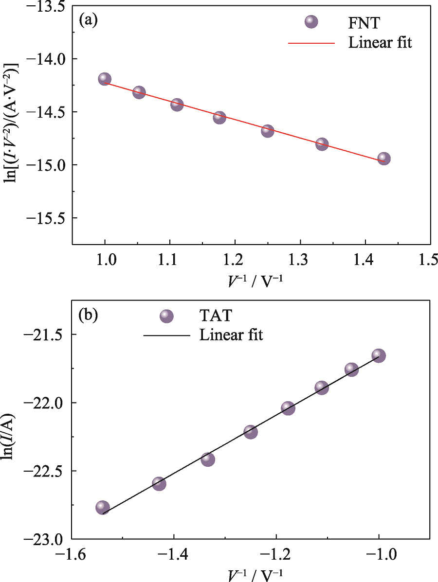
Fig. 6 Fitting of tunneling mechanism for FTD (5 nm) (a) ln(I/V2) vs. V-1 plots with FNT fitting under positive voltage; (b) lnI vs. V-1 plots with TAT fitting under negative voltage
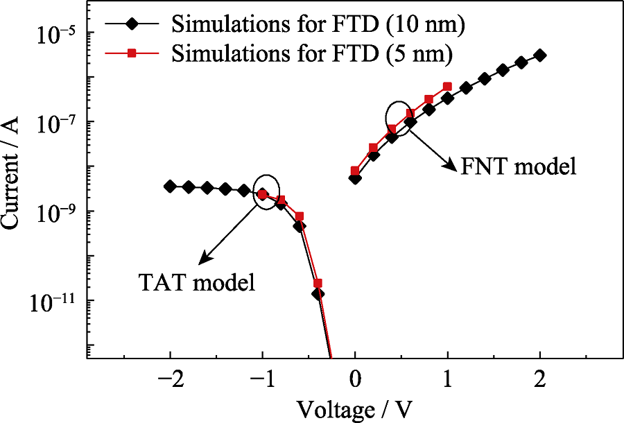
Fig. 7 I-V curves obtained from TCAD simulations for TiN/ZnO/Pt FTDs with tunneling distances of 10 and 5 nm, analyzed using the FNT model under positive bias and the TAT model under negative bias
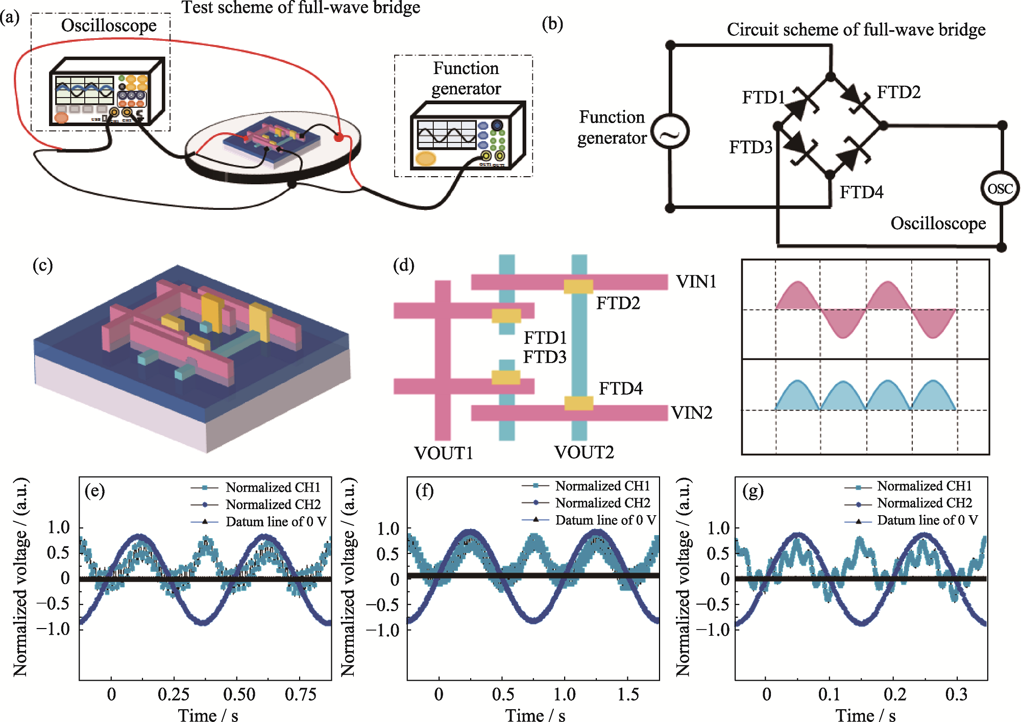
Fig. 8 Scheme and experiment for full-wave rectifier bridge (a) Test scheme for full-wave rectifier bridge; (b) Circuit scheme for full-wave rectifier bridge; (c) Structure schematic of full-wave rectifier bridge; (d) Layout diagram of full wave rectifier circuit (left) and corresponding rectification result (right); (e-g) Normalized full-wave rectification results of full-wave rectifier based on the TiN/ZnO/Pt FTDs with Vpp=1.5 V at frequencies of 1 (e), 2 (f) and 5 Hz (g), respectively
| Parameter | Description | Unit | Value |
|---|---|---|---|
| TOX | Thickness of tunneling layer | Å | 100 |
| IF | Forward Fowler-Nordheim current coefficient | A/V2 | 5×10-16 |
| IR | Reverse Fowler-Nordheim current coefficient | A/V2 | 1×10-16 |
| EF | Forward critical electric field | V/cm | 2×10⁶ |
| ER | Reverse critical electric field | V/cm | 2×10⁸ |
| L | Diode length | m | 2×10⁻⁸ |
| W | Diode width | m | 5×10⁻⁴ |
Table 2 Parameters of the ideal physical model of FTD
| Parameter | Description | Unit | Value |
|---|---|---|---|
| TOX | Thickness of tunneling layer | Å | 100 |
| IF | Forward Fowler-Nordheim current coefficient | A/V2 | 5×10-16 |
| IR | Reverse Fowler-Nordheim current coefficient | A/V2 | 1×10-16 |
| EF | Forward critical electric field | V/cm | 2×10⁶ |
| ER | Reverse critical electric field | V/cm | 2×10⁸ |
| L | Diode length | m | 2×10⁻⁸ |
| W | Diode width | m | 5×10⁻⁴ |
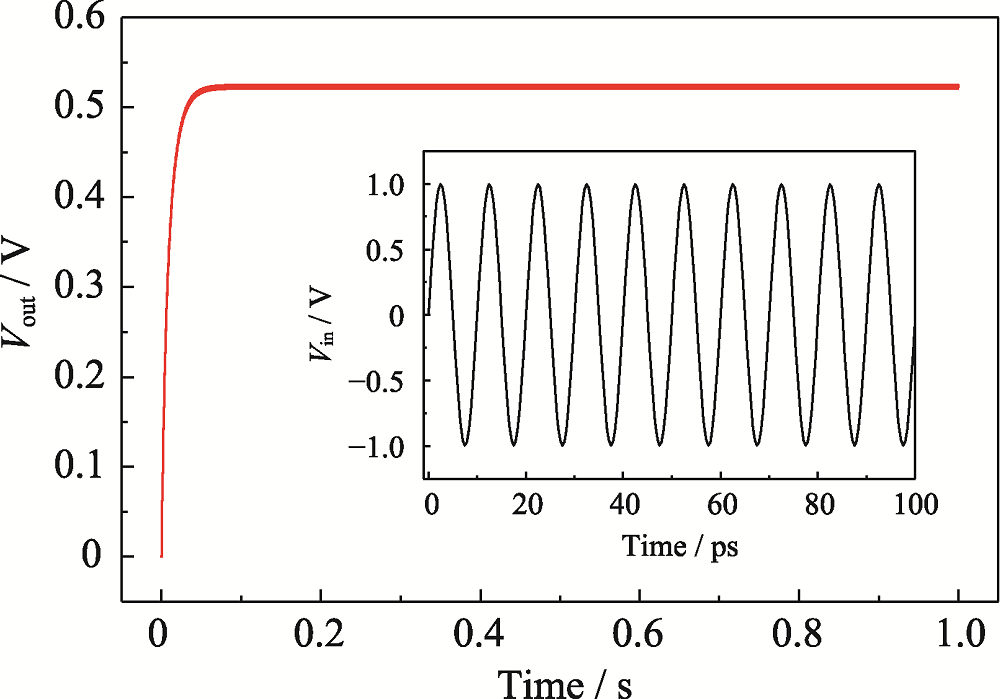
Fig. 9 SPICE simulations for the full-wave rectifier bridge based FTDs with a frequency of 100 GHz and Vpp=2 V
| [1] |
KHAN A A, JAYASWAL G, GAHAFFAR F A, et al. Metal- insulator-metal diodes with sub-nanometre surface roughness for energy-harvesting applications. Microelectron. Eng., 2017, 181: 34.
DOI URL |
| [2] |
DRAGOMAN M, ALDRIGO M. Graphene rectenna for efficient energy harvesting at terahertz frequencies. Appl. Phys. Lett., 2016, 109(11): 113105.
DOI URL |
| [3] |
OLLER D, OSGOOD R, XU J, et al. Optical rectification in a reconfigurable resistive switching filament. Appl. Phys. Lett., 2019, 115(4): 043101.
DOI URL |
| [4] |
WEERAKKODY A, BELKADI A, MODDEL G. Nonstoichiometric nanolayered Ni/NiO/Al2O3/CrAu metal-insulator-metal infrared rectenna. ACS Appl. Nano Mater., 2021, 4(3): 2470.
DOI URL |
| [5] |
BELKADI A, WEERAKKODY A, MODDEL G. Demonstration of resonant tunneling effects in metal-double-insulator-metal (MI(2)M) diodes. Nat. Commun., 2021, 12: 2925.
DOI |
| [6] |
SHAYGAN M, WANG Z, ELSAYED M S, et al. High performance metal-insulator-graphene diodes for radio frequency power detection application. Nanoscale, 2017, 9(33): 11944.
DOI PMID |
| [7] |
SANCHEZ A, DAVIS C F, LIU K C, et al. The MOM tunneling diode: theoretical estimate of its performance at microwave and infrared frequencies. J. Appl. Phys., 1978, 49(10): 5270.
DOI URL |
| [8] |
NISHIDA Y, NISHIGAMI N, DIEBOLD S, et al. Terahertz coherent receiver using a single resonant tunnelling diode. Sci. Rep., 2019, 9: 18125.
DOI PMID |
| [9] |
MITROVIC I Z, ALMALKI S, TEKIN S B, et al. Oxides for rectenna technology. Materials, 2021, 14(18): 5218.
DOI URL |
| [10] |
ALSHEHRI A H, MISTRY K, NGUYEN V H, et al. Quantum- tunneling metal-insulator-metal diodes made by rapid atmospheric pressure chemical vapor deposition. Adv. Funct. Mater., 2018, 29(7): 1805533.
DOI URL |
| [11] |
ANDERSON E C, BOUGHER T L, COLA B A. High performance multiwall carbon nanotube-insulator-metal tunnel diode arrays for optical rectification. Adv. Electron. Mater., 2018, 4(3): 1700446.
DOI URL |
| [12] |
ALSHEHRI A H, SHAHIN A, MISTRY K, et al. Metal- insulator-insulator-metal diodes with responsivities greater than 30 A·W-1 based on nitrogen-doped TiOx and AlOx insulator layers. Adv. Electron. Mater., 2021, 7(11): 2100467.
DOI URL |
| [13] |
ALIMARDANI N, CONLEY J F. Enhancing metal-insulator- insulator-metal tunnel diodes via defect enhanced direct tunneling. Appl. Phys. Lett., 2014, 105(8): 082902.
DOI URL |
| [14] |
SHRIWASTAVA S, TRIPATHI C C. Metal-insulator-metal diodes: a potential high frequency rectifier for rectenna application. J. Electron. Mater., 2019, 48(5): 2635.
DOI |
| [15] | ZHANG X, GRAJAL J, VAZQUEZ-ROY J L, et al. Two- dimensional MoS2-enabled flexible rectenna for Wi-Fi-band wireless energy harvesting. Nature, 2019, 566(7744): 368. |
| [16] |
HOLDEN K E K, QI Y, CONLEY J F. Precision defect engineering of metal/insulator/metal diodes using atomic layer deposition to localize Ni impurities in Al2O3 tunnel barriers. J. Appl. Phys., 2021, 129(14): 144502.
DOI URL |
| [17] |
SINGH A, RATNADURAI R, KUMAR R, et al. Fabrication and current-voltage characteristics of NiOx/ZnO based MIIM tunnel diode. Appl. Surf. Sci., 2015, 334: 197.
DOI URL |
| [18] | RATNADURAI R, KRISHNAN S, STEFANAKOS E, et al. Nanomanufacturability of thin film MIM diodes. AIP Conference Proceedings, 2010, 1313: 403. |
| [19] |
PERIASAMY P, BERRY J J, DAMERON A A, et al. Fabrication and characterization of MIM diodes based on Nb/Nb2O5 via a rapid screening technique. Adv. Mater., 2011, 23(27): 3080.
DOI URL |
| [20] | PERIASAMY P, GUTHREY H L, ABDULAGATOV A I, et al. Metal-insulator-metal diodes: role of the insulator layer on the rectification performance. Adv. Mater., 2013, 25(9): 1301. |
| [21] |
MISTRY K, YAVUZ M, MUSSELMAN K P. Simulated electron affinity tuning in metal-insulator-metal (MIM) diodes. J. Appl. Phys., 2017, 121(18): 184504.
DOI URL |
| [22] |
OZYIGIT D, ULLAH F, GULSARAN A, et al. Manufacturing of quantum-tunneling MIM nanodiodes via rapid atmospheric CVD in terahertz band. Sci. Rep., 2023, 13(1): 20733.
DOI |
| [23] |
WARD D R, HUSER F, PAULY F, et al. Optical rectification and field enhancement in a plasmonic nanogap. Nat. Nanotechnol., 2010, 5(10): 732.
DOI PMID |
| [24] |
LIU Z, ABE S, SHIMIZU M, et al. Enhanced current density and asymmetry of metal-insulator-metal diodes based on self-assembly of Pt nanoparticles. Appl. Phys. Lett., 2023, 122(9): 093502.
DOI URL |
| [25] |
HERNER S B, WEERAKKODY A D, BELKADI A, et al. High performance MIIM diode based on cobalt oxide/titanium oxide. Appl. Phys. Lett., 2017, 110(22): 223901.
DOI URL |
| [26] |
MITROVIC I Z, WEERAKKODY A D, SEDGHI N, et al. Controlled modification of resonant tunneling in metal-insulator- insulator-metal structures. Appl. Phys. Lett., 2018, 112(1): 012902.
DOI URL |
| [27] |
ALSHEHRI A H, ASGARIMOGHADDAM H, DELUMEAU L V, et al. Combinatorial optimization of metal-insulator-insulator-metal (MIIM) diodes with thickness-gradient films via spatial atomic layer deposition. Adv. Electron. Mater., 2024, 10(11): 2400093.
DOI URL |
| [28] |
FENG G, ZHU Q, LIU X, et al. A ferroelectric fin diode for robust non-volatile memory. Nat. Commun., 2024, 15: 513.
DOI PMID |
| [29] |
LIU X, FENG G, FENG X, et al. Ultrahigh rectification ratio in an asymmetric metal/semiconductor/metal nanoscale tunneling junction: implications for high-frequency rectifiers. ACS Appl. Nano Mater., 2023, 6(4): 2491.
DOI URL |
| [30] |
LIU H, ZHANG L, LEBEGUE S, et al. Morphology-electronic effects in ultra-model nanocatalysts under the CO oxidation reaction: the case of ZnO ultrathin films grown on Pt(111). Nanoscale, 2024, 16(43): 20216.
DOI URL |
| [31] |
CHEN T, YU K, HU H, et al. Engineering electron transport layer with ionic liquid for high-performance quantum dot light-emitting diodes. ACS Appl. Nano Mater., 2025, 8(9): 4573.
DOI URL |
| [32] |
SHINDE P, HASE Y, DOIPHODE V, et al. Morphology-dependent ZnO/MoS2 heterostructures for enhanced photoelectrochemical water splitting. ACS Appl. Energ. Mater., 2025, 8(2): 935.
DOI URL |
| [33] |
ALIMARDANI N, KING S W, FRENCH B L, et al. Investigation of the impact of insulator material on the performance of dissimilar electrode metal-insulator-metal diodes. J. Appl. Phys., 2014, 116(2): 024508.
DOI URL |
| [34] |
CONG X, ZHENG Y, HUANG F, et al. Efficiently band-tailored type-Ⅲ van der Waals heterostructure for tunnel diodes and optoelectronic devices. Nano Res., 2022, 15(9): 8442.
DOI |
| [35] |
LEE G H, YU Y J, LEE C, et al. Electron tunneling through atomically flat and ultrathin hexagonal boron nitride. Appl. Phys. Lett., 2011, 99(24): 243114.
DOI URL |
| [36] |
MA Q, ANDERSEN T I, NAIR N L, et al. Tuning ultrafast electron thermalization pathways in a van der Waals heterostructure. Nat. Phys., 2016, 12(5): 455.
DOI |
| [37] |
VU Q A, LEE J H, NGUYEN V L, et al. Tuning carrier tunneling in van der waals heterostructures for ultrahigh detectivity. Nano Lett., 2017, 17(1): 453.
DOI PMID |
| [38] |
TEKIN S B, ALMALKI S, FINCH H, et al. Electron affinity of metal oxide thin films of TiO2, ZnO, and NiO and their applicability in 28.3 THz rectenna devices. J. Appl. Phys., 2023, 134(8): 084503.
DOI URL |
| [39] | FOWLER R H, NORDHEIM L. Electron emission in intense electric fields. Proc. Roy. Soc. A, 1928, 119(791): 173. |
| [40] |
YU S, GUAN X, WONG H S P. Conduction mechanism of TiN/HfOx/Pt resistive switching memory: a trap-assisted-tunneling model. Appl. Phys. Lett., 2011, 99(6): 063507.
DOI URL |
| [41] |
CHANG W J, HOUNG M P, WANG Y H. Electrical properties and modeling of ultrathin impurity-doped silicon dioxides. J. Appl. Phys., 2001, 90(10): 5171.
DOI URL |
| [42] |
TSIARAPAS C, GIRGINOUDI D, DIMITRIADIS E I, et al. Investigation on deep level defects in polycrystalline ZnO thin films. J. Vac. Sci. Technol. B, 2017, 35(3): 031203.
DOI URL |
| [1] | HONG Enliu, TU Xinchen, LI Ziqing, FANG Xiaosheng. Two-dimensional Perovskite Single Crystal Nanosheets: Floating Growth and Optoelectronic Performance [J]. Journal of Inorganic Materials, 2026, 41(6): 787-794. |
| [2] | WANG Mengmeng, TIAN Li, ZHANG Junmin, LI Qinggang, YANG Jinshan, DONG Shaoming. Highly Efficient EMI Shielding via 3D-printed CNT/SiC-SiO2 Architectures [J]. Journal of Inorganic Materials, 2026, 41(6): 831-838. |
| [3] | LI Hantao, SHEN Qiang, LUO Guoqiang, WANG Xuefei, GAO Ming, CHEN Chen. Research Progress on Structure and Performance Regulation of Silicon-based Anode Materials via Mechanical Ball Milling [J]. Journal of Inorganic Materials, 2026, 41(5): 561-572. |
| [4] | QIAN Xinyu, WANG Wudi, GUO Junyao, REN Yongchun, DONG Jianshu, WANG Qingguo, TANG Huili, ZHANG Chenbo, XU Xiaodong, DONG Yongjun, HUA Wei, XU Jun. Spectroscopic Analysis of Ho:BaF2 Crystals in the NIR to MIR Spectral Region [J]. Journal of Inorganic Materials, 2026, 41(5): 595-603. |
| [5] | ZHU Kaihuang, YANG Shijie, LI Xinge, SONG Guanqing, SHI Gansheng, WANG Yan, REN Xiaomeng, LU Yao, XU Xinhong, SUN Jing. Graphene Oxide Modified UiO-66 Based Metal Organic Framework Gel: Preparation and Efficient Toluene Adsorption Performance [J]. Journal of Inorganic Materials, 2026, 41(4): 519-526. |
| [6] | JIANG Shengnan, ZHENG Zhong, HE Weiyi, LIU Tao, PAN Xiuhong, CHEN Kun, GUO Hui, GAO Pan, LIU Chunjun, LIU Xuechao. Preparation and Performance Optimization of Boron-gallium Co-doped Zinc Oxide Transparent Electrodes [J]. Journal of Inorganic Materials, 2026, 41(4): 479-485. |
| [7] | XU Hao, GU Haitao, WU Honghui, YUE Xiaofei, LIN Siqi, JIN Min. Crystal Growth and Properties of Bi-doped InSe [J]. Journal of Inorganic Materials, 2026, 41(4): 493-499. |
| [8] | ZHANG Mengjie, LI Zhibo, HUANG Ruinan, LÜ Xiangfei, WANG Wei. Cordierite/Aluminum Borate Whiskers/Co0.8FexCe0.2-xCr2O4 Catalysts: Preparation and Filtration Catalytic Performance for Carbon Soot [J]. Journal of Inorganic Materials, 2026, 41(4): 509-518. |
| [9] | SUI Jinyang, ZHOU Dayu, ZHAO Wenjin, TONG Yi, WANG Xinpeng. Effects of Working Pressure on the Structure and Electrical Properties of AlScN Thin Films [J]. Journal of Inorganic Materials, 2026, 41(4): 486-492. |
| [10] | CHENG Aopeng, WANG Yuewen, XU Wentao, LIU Quanwei, ZHANG Haitao, ZHOU Youfu. Fabrication of Graphene-reinforced Alumina Ceramic Composites via Adsorption-precipitation Self-assembly Combined with Spark Plasma Sintering [J]. Journal of Inorganic Materials, 2026, 41(4): 536-544. |
| [11] | LI Xuan, YE Kuicai, FENG Jiayin, QIU Jiajun, QIAN Wenhao, XING Min. Surface Modification of Titanium-based Dental Implants for Soft Tissue Sealing: A Review [J]. Journal of Inorganic Materials, 2026, 41(4): 432-444. |
| [12] | WANG Yuhe, LUO Yixiu, GUO Huiming, ZHANG Guangheng, ZHANG Siyan, SUN Luchao, WANG Jiemin, WANG Jingyang. First-principles Investigation of Elastic and Thermophysical Properties of High-entropy Rare-earth Oxide Thermal Barrier Coating Materials [J]. Journal of Inorganic Materials, 2026, 41(4): 445-454. |
| [13] | LI Zexi, LU Wenjie, WANG Chao, ZHANG Lu, LI Shuti, GAO Fangliang. Two-dimensional GaN: Preparation Based on Liquid Metal Gallium and Photoelectric Properties [J]. Journal of Inorganic Materials, 2026, 41(3): 377-384. |
| [14] | TIAN Hongwang, LUO Longfei, HU Chenglong, YAN Meng, PANG Shengyang, LI Jian, TANG Sufang. Facile Fabrication of Ceramic-resin Coatings on C/CA Composites for Oxidation Protection at Medium Temperatures [J]. Journal of Inorganic Materials, 2026, 41(3): 401-408. |
| [15] | CAO Juan, WU Xishi, LIU Zehua, PEI Bingbing, HAN Jianshen, LIU Huan, YANG Yitian, WU Haibo, HUANG Zhengren. Influence of Grain Size on Weibull Distribution of Fracture Strength in Atmospheric-pressure Solid-phase Sintered SiC Ceramics [J]. Journal of Inorganic Materials, 2026, 41(2): 217-224. |
| Viewed | ||||||
|
Full text |
|
|||||
|
Abstract |
|
|||||
