Journal of Inorganic Materials ›› 2025, Vol. 40 ›› Issue (11): 1188-1200.DOI: 10.15541/jim20250094
Special Issue: 【信息功能】透明与闪烁陶瓷(202512); 【信息功能】功能晶体(202512)
• REVIEW • Previous Articles Next Articles
LI Chengming( ), ZHOU Chuang, LIU Peng, ZHENG Liping, LAI Yongji, CHEN Liangxian, LIU Jinlong, WEI Junjun
Received:2025-03-05
Revised:2025-03-31
Published:2025-11-20
Online:2025-04-24
About author:LI Chengming (1962-), male, professor. E-mail: chengmli@mater.ustb.edu.cn
CLC Number:
LI Chengming, ZHOU Chuang, LIU Peng, ZHENG Liping, LAI Yongji, CHEN Liangxian, LIU Jinlong, WEI Junjun. Stress in CVD Diamond Films: Generation, Suppression, Application, and Measurement[J]. Journal of Inorganic Materials, 2025, 40(11): 1188-1200.
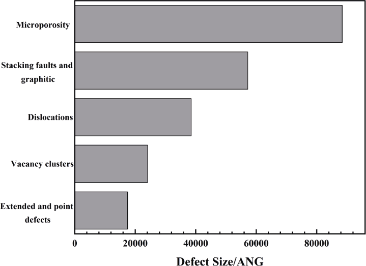
Fig. 1 Comparison of different types of defect sizes[11]
| Substrate material | Elastic modulus/GPa | Melting temperature/K | Coefficient of thermal expansion (polynomial interpolation)/(×10-6, K-1) |
|---|---|---|---|
| Si | 130 | 1683 | -2.15+2.47×10⁻²T-3.82×10⁻⁵T2+2.67×10⁻⁸T3-6.87×10⁻¹²T4 |
| Mo | 327 | 2888 | 4.31+0.002T |
| W | 411 | 3660 | 2.78+0.01T-2.21×10⁻⁵T2+1.93×10⁻⁸T3-5.56×10⁻¹²T4 |
| Diamond | 1050 | — | -1.36+8.79×10⁻³T+3.98×10⁻⁷T²-6.18×10⁻⁹T³+2.78×10⁻¹²T4 |
Table 1 Thermal expansion coefficients of common substrate materials[12]
| Substrate material | Elastic modulus/GPa | Melting temperature/K | Coefficient of thermal expansion (polynomial interpolation)/(×10-6, K-1) |
|---|---|---|---|
| Si | 130 | 1683 | -2.15+2.47×10⁻²T-3.82×10⁻⁵T2+2.67×10⁻⁸T3-6.87×10⁻¹²T4 |
| Mo | 327 | 2888 | 4.31+0.002T |
| W | 411 | 3660 | 2.78+0.01T-2.21×10⁻⁵T2+1.93×10⁻⁸T3-5.56×10⁻¹²T4 |
| Diamond | 1050 | — | -1.36+8.79×10⁻³T+3.98×10⁻⁷T²-6.18×10⁻⁹T³+2.78×10⁻¹²T4 |
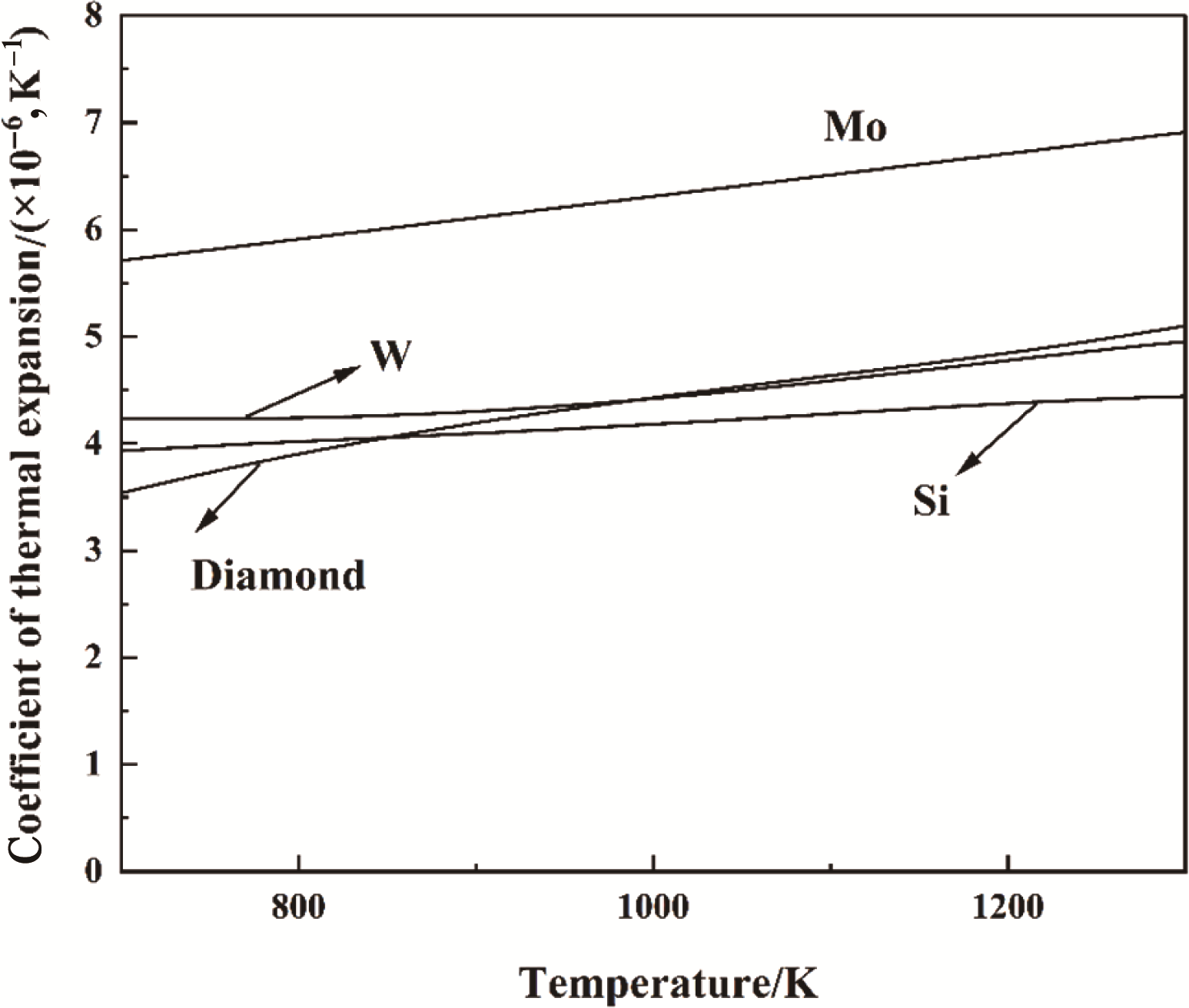
Fig. 2 Relationship between coefficient of thermal expansion and temperature of common substrate materials[12]
| Material | Si (0.543 nm) | Mo (0.3147 nm) | W (0.3165 nm) | Diamond (0.357 nm) |
|---|---|---|---|---|
| Lattice mismatch | 34.3% | 13.4% | 12.8% | — |
Table 2 Lattice constants and lattice mismatch of diamond with various materials
| Material | Si (0.543 nm) | Mo (0.3147 nm) | W (0.3165 nm) | Diamond (0.357 nm) |
|---|---|---|---|---|
| Lattice mismatch | 34.3% | 13.4% | 12.8% | — |
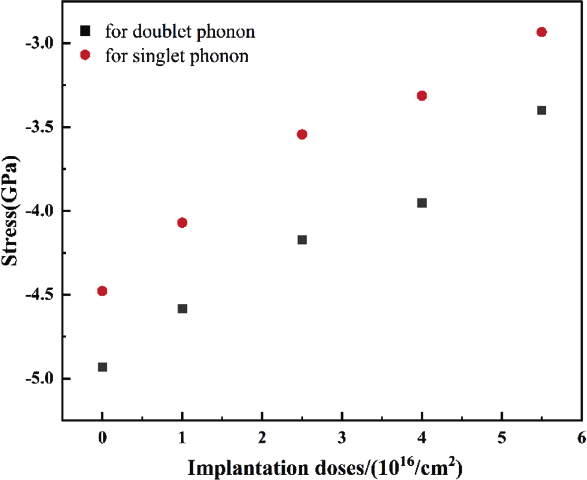
Fig. 3 Relationship between carbon ion implantation dose and stress[47]
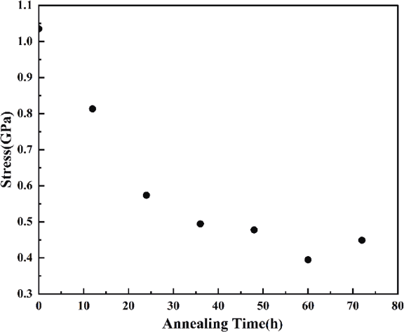
Fig. 4 Relationship between annealing time and stress[16]
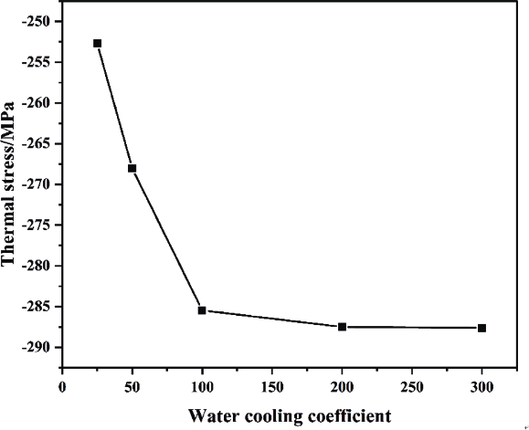
Fig. 5 Relationship between water cooling coefficient and thermal stress[58]
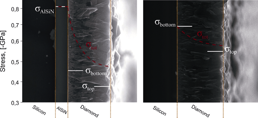
Fig. 6 Distribution of the total stress σtot in the system and the stress σAlSiN in the Al-Si-N intermediate layer, as well as the bottom and top stress (σbottom, σtop) of the diamond film[62]
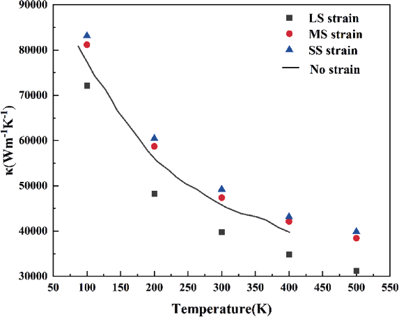
Fig. 7 Temperature dependence of κ under uniaxial tensile stress at different scales[66]
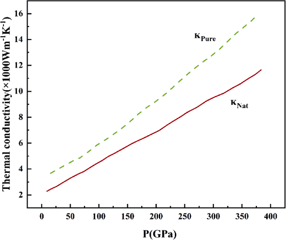
Fig. 8 Thermal conductivity κNat and κPure of natural diamond and pure diamond varied with pressure at 300 K[67]
| [1] |
INYUSHKIN A V, TALDENKOV A N, RALCHENKO V G, et al. Thermal conductivity of high purity synthetic single crystal diamonds. Physical Review B, 2018, 97(14): 144305.
DOI URL |
| [2] | MARTIN H, REINTJES M, REIJS D, et al. Heterogeneous integration of diamond heat spreaders for power electronics application. IEEE 73rd Electronic Components and Technology Conference (ECTC), Orlando, 2023: 118-125. |
| [3] |
HOTCHANDANI V, MATHEW B, YESUDASAN S, et al. Thermo-hydraulic characteristics of novel MEMS heat sink. Microsystem Technologies, 2021, 27(1): 145.
DOI |
| [4] |
LEE V Y S, KARAYIANNIS T G. Effect of inlet subcooling on flow boiling in microchannels. Applied Thermal Engineering, 2020, 181: 115966.
DOI URL |
| [5] | SHAPIRA S, NIRENBERG N. Performance envelope enabled by CVD diamond heatspreader integration in semiconductor chips. IEEE International Conference on Microwaves, Communications, Antennas, Biomedical Engineering and Electronic Systems (COMCAS), Tel Aviv, 2024: 1-6. |
| [6] | SHAPIRA S. Performance enhancement of integrated circuits and power devices via embedded diamond heat management. IEEE International Conference on Microwaves, Antennas, Communications and Electronic Systems (COMCAS), Tel Aviv, 2021: 470-472. |
| [7] | LIU C. Stress response and physical properties of diamondunder complex strain. Changchun: PhD thesis of Jilin University, 2020. |
| [8] |
ZHANG S L, YE Z H, ZHU Y, et al. Enhanced optical properties of CVD diamond through HPHT annealing. Crystal Growth & Design, 2024, 24(16): 6701.
DOI URL |
| [9] |
FERREIRA N G, ABRAMOF E, CORAT E J, et al. Residual stresses and crystalline quality of heavily boron-doped diamond films analysed by micro-Raman spectroscopy and X-ray diffraction. Carbon, 2003, 41(6): 1301.
DOI URL |
| [10] | HUANG Y S, LOU C P, QIU W Q. Crystal defects and impurities of CVD diamond films. China Surface Engineering, 2004(1):5. |
| [11] | GRAY K J, WINDISCHMANN H. Free-standing CVD diamond wafers for thermal management by d.c. arc jet technology. Diamond & Related Materials, 1999, 8(2-5): 903. |
| [12] |
JEONG J H, LEE S Y, LEE W S, et al. Mechanical analysis for crack-free release of chemical-vapor-deposited diamond wafers. Diamond and Related Materials, 2002, 11(8): 1597.
DOI URL |
| [13] |
LEIGH W G S, CUENCA J A, THOMAS E L H, et al. Mapping the effect of substrate temperature inhomogeneity during microwave plasma-enhanced chemical vapour deposition nanocrystalline diamond growth. Carbon, 2023, 201: 328.
DOI URL |
| [14] | GEORGE C. Numerical simulation of a multicomponent non-transferred constricted direct current arc with a supersonic plasma jet. Minnesota: PhD thesis of University of Minnesota, 1998. |
| [15] | FAN Y D, ZHOU Z F. Crystal defects and impurities of CVD diamond films. Journal of Materials Science and Engineering (Materials Science & Engineering), 1996(1): 5. |
| [16] | NAKAMURA Y, SAKAGAMI S, AMAMOTO Y, et al. Measurement of internal stresses in CVD diamond films. Thin Solid Films, 1997, 308: 249. |
| [17] | SCARDI P, LEONI M, SESSA V, et al. Residual stress in diamond coatings by synchrotron radiation XRD. European Powder Diffraction: Epdic Iv, Pts 1 and 2, Stafa-Zurich, 1996: 451-456. |
| [18] |
WENG J, LIU F, XIONG L W, et al. Deposition of large area uniform diamond films by microwave plasma CVD. Vacuum, 2018, 147: 134.
DOI URL |
| [19] |
SCHRECK M, BAUR T, FEHLING R, et al. Modification of diamond film growth by a negative bias voltage in microwave plasma chemical vapor deposition. Diamond and Related Materials, 1998, 7(2-5): 293.
DOI URL |
| [20] |
LIU P, SHAO S, YANG Z, et al. The uniform and robust 8-inch CVD diamond plate generated by dual-magnetic field controlled DC Jet CVD. Diamond and Related Materials, 2024, 141: 110670.
DOI URL |
| [21] |
HUANG Y, CHEN L, SHAO S, et al. The 7-in. freestanding diamond thermal conductive film fabricated by DC arc plasma jet CVD with multi-stage magnetic fields. Diamond and Related Materials, 2022, 122: 108812.
DOI URL |
| [22] |
FERREIRA N G, ABRAMOF E, LEITE N F, et al. Analysis of residual stress in diamond films by X-ray diffraction and micro-Raman spectroscopy. Journal of Applied Physics, 2002, 91(4): 2466.
DOI URL |
| [23] |
LONG F, WEI Q P, YU Z M, et al. Effects of temperature and Mo2C layer on stress and structural properties in CVD diamond film grown on Mo foil. Journal of Alloys and Compounds, 2013, 579: 638.
DOI URL |
| [24] |
WOEHRL N, HIRTE T, POSTH O, et al. Investigation of the coefficient of thermal expansion in nanocrystalline diamond films. Diamond and Related Materials, 2009, 18(2/3): 224.
DOI URL |
| [25] | YANG J X, LI C M, CHEN G C, et al. Analysis of residual stress distribution in DC arc plasma jet CVD high quality diamond films by Raman spectroscopy. Journal of Synthetic Crystals, 2004(4): 674. |
| [26] | DAI X N, BAI L, SUN W Y, et al. Study on the preparation technology of diamond film by MPCVD. Superhard Material Engineering, 2022, 34(2): 36. |
| [27] |
WOEHRL N, BUCK V. Influence of hydrogen on the residual stress in nanocrystalline diamond films. Diamond and Related Materials, 2007, 16(4-7): 748.
DOI URL |
| [28] | YAMADA H. Numerical simulations to study growth of single- crystal diamond by using microwave plasma chemical vapor deposition with reactive (H, C, N) species. Japanese Journal of Applied Physics, 2012, 51(9): 105. |
| [29] | LIANG T. Study on high quality diamond prepared by high pressure MPCVD. Wuhan: Master Thesis of Wuhan Institute of Technology, 2018. |
| [30] |
SALGUEIREDO E, AMARAL M, NETO M A, et al. HFCVD diamond deposition parameters optimized by a Taguchi Matrix. Vacuum, 2011, 85(6): 701.
DOI URL |
| [31] | ZHU H X, MAO W M, FENG H P. Influence of texture on residual strain in CVD free standing diamond films. Chinese Journal of Materials Research, 2007(1): 32. |
| [32] | ZHOU Z Y, CHEN G C, ZHOU Y L, et al. Controlling deposition and roughness of free-standing diamond film deposited by DC plasma jet CVD. Journal of Synthetic Crystals, 2005(1): 21. |
| [33] | LI R B. Study of the stress in doped CVD diamond films. Acta Physica Sinica, 2007(6): 3428. |
| [34] |
MAO W M, ZHU H X, CHEN L, et al. Relationship between texture and residual macro-strain in CVD diamond films based on phenomenological analysis. Journal of University of Science and Technology Beijing, 2008, 15(2): 197.
DOI URL |
| [35] |
IKEDA R, UCHIYAMA T, CHO H, et al. An advanced method for measuring the residual stress of deposited film utilizing laser spallation technique. Science and Technology of Advanced Materials, 2006, 7(1): 90.
DOI URL |
| [36] |
TSUJI T, SHINEI C, IWASAKI T, et al. Evaluation of stress in (111) homoepitaxial CVD diamond films by Raman spectrum and nitrogen- vacancy centers. Applied Physics Express, 2024, 17(11): 115502.
DOI |
| [37] | HE J S, ZHANG M, XIAO Q. Calculation of the lattice mismatch between semiconductor epitaxy and substrate. Journal of Nanchang University Natural Science, 2006, 30(1): 63. |
| [38] | NIU D C, LI C M, LIU Z, et al. Growth stability and quality of plasma jet CVD diamond films under gas recycling condition. Journal of University Science and Technology Beijing, 2007, 29(11): 1133. |
| [39] |
TACHIBANA T, YOKOTA Y, HAYASHI K, et al. Parametric study of bias-enhanced nucleation of diamond on platinum in microwave plasma. Diamond and Related Materials, 2000, 9(3-6): 251.
DOI URL |
| [40] |
NIU C M, TSAGAROPOULOS G, BAGLIO J, et al. Nucleation and growth of diamond on Si, Cu, and Au substrates. Journal of Solid State Chemistry, 1991, 91(1): 47.
DOI URL |
| [41] |
CHIU K A, WU P H, WANG W L, et al. Homoepitaxial overgrowth of (111) diamond films on Au-coated and Ni-coated substrates. Surface and Coatings Technology, 2022, 437: 128348.
DOI URL |
| [42] |
KHAN M A, HAQUE M S, NASEEM H A, et al. Microwave plasma chemical vapor deposition of diamond films with low residual stress on large area porous silicon substrates. Thin Solid Films, 1998, 332(1/2): 93.
DOI URL |
| [43] | ZHANG Y Y, ZHANG D L, ZHANG L B, et al. The effect of surface roughness of seed on the high-rate homoepitaxial growth of CVD single-crystal diamonds. Applied Physics A-Materials Science & Processing, 2023, 129(6): 415. |
| [44] |
SILVA F, ACHARD J, BRINZA O, et al. High quality, large surface area, homoepitaxial MPACVD diamond growth. Diamond and Related Materials, 2009, 18(5-8): 683.
DOI URL |
| [45] | MARTINEAU P M, LAWSON S C, TAYLOR A J, et al. Identification of synthetic diamond grown using chemical vapor deposition (CVD). Gems & Gemology, 2004, 40(1): 2. |
| [46] |
GAUKROGER M P, MARTINEAU P M, CROWDER M J, et al. X-ray topography studies of dislocations in single crystal CVD diamond. Diamond and Related Materials, 2008, 17(3): 262.
DOI URL |
| [47] | XIA Y B, WANG L J. Diamond film/alumina composites used as the packaging material in integrated circuits with ultra-high speed and high power. 6th IEEE CPMT Conference on High Density Microsystem Design and Packaging and Component Failure Analysis (HDP 04), Shanghai, 2004: 367-372. |
| [48] |
ITO S, NAGAI M, MATSUMOTO T, et al. Self-separation of freestanding diamond films using graphite interlayers precipitated from C-dissolved Ni substrates. Journal of Crystal Growth, 2017, 470: 104.
DOI URL |
| [49] |
MATTHIEU J. VERSTRAETE J C C. Why is iridium the best substrate for single crystal diamond growth? Applied Physics Letters, 2005, 86(191): 191917.
DOI URL |
| [50] | REDDY P R S, JANARDHANAM V, REDDY V R, et al. Effects of rapid thermal annealing on the structural, optical, and electrical properties of Au/CuPc/n-Si (MPS)-type Schottky barrier diodes. Applied Physics A-Materials Science & Processing, 2021, 127(10): 803. |
| [51] | PAVANI M, KUMAR A A, REDDY V R, et al. Optical, morphological and electrical properties of rapid thermally annealed CoPc/n-Ge heterostructures for photodiode applications. Materials Science and Engineering B-Advanced Functional Solid-State Materials, 2024, 300: 117102. |
| [52] |
FENG C Q, WU L, CHEN P, et al. Repairing slight damages on monocrystalline silicon surface by thermal annealing. Materials Research Express, 2021, 8(4): 045005.
DOI |
| [53] |
WU J M, HE Z, GUO Z Y, et al. Pulsed laser annealing of phosphorous-implanted 4H-SiC: electrical and structural characteristics. Journal of Electronic Materials, 2022, 51(1): 172.
DOI |
| [54] |
YANG T, XIA Z L, FAN D Y, et al. Activation enhancement and grain size improvement for poly-Si channel vertical transistor by laser thermal annealing in 3D NAND Flash. Micromachines, 2023, 14(1): 230.
DOI URL |
| [55] |
JACOBS A G, FEIGELSON B N, SPENCER J A, et al. Efficient activation and high mobility of ion-implanted silicon for next-generation GaN devices. Crystals, 2023, 13(5): 736.
DOI URL |
| [56] | NIJHAWAN S, RANKIN J, WALDEN B L, et al. Grain impingement and intrinsic stresses in CVD diamond. Symposium on Thin-Films-Stresses and Mechanical Properties VII at the MRS Fall Meeting, Boston, 1997: 415-420. |
| [57] | YAN X B. Graphitization behavior of CVD free-standing diamond films at high temperature. Beijing: PhD thesis of University of Science &Technology Beijing, 2019. |
| [58] | XU F, ZUO D W, LU W Z, et al. Study of the thermal and intrinsic stress of large area diamond film prepared by HFCVD. 9th Conference on Machining and Advanced Manufacturing Technology in China, Harbin, 2007: 123-127. |
| [59] | YANG C, LIU D, ZHU F, et al. Method for reducing crack of diamond film, involves controlling substrate column to be separated from cooling table placed under substrate column until cooling is completed, in cooling process after growth is completed, when temperature of substrate column is lowered to set temperature: CN113684466-A; CN113684466-B. 2021-11-23; 2022-01-25. |
| [60] |
CHANG Y Y, YANG Y J, WENG S Y. Effect of interlayer design on the mechanical properties of AlTiCrN and multilayered AlTiCrN/ TiSiN hard coatings. Surface & Coatings Technology, 2020, 389: 125637.
DOI URL |
| [61] |
LIU L L, RUAN Q D, WU Z Z, et al. Fabrication and cutting performance of CrAlN/CrAl multilayer coatings deposited by continuous high-power magnetron sputtering. Ceramics International, 2022, 48(10): 14528.
DOI URL |
| [62] |
GAYDAYCHUK A, ZENKIN S, LINNIK S. Influence of Al-Si-N interlayer on residual stress of CVD diamond coatings. Surface & Coatings Technology, 2019, 357: 348.
DOI URL |
| [63] | DU Y, YAN B, LI H, et al. Method for preparing low stress diamond film by using ultrasonic cavitation technology to synthesize metal gallium buffer layer in medical fields, involves adding liquid gallium into ethanol, performing ultrasonic treatment, and taking supernatant to obtain metal gallium nano-particle suspension: CN117026201-A. 2023-11-10. |
| [64] |
GUO J C, LIU J L, HUA C Y, et al. Interfacial stress evolution simulation on the graphite substrate/interlayer/diamond film during the cooling process. Diamond and Related Materials, 2017, 75: 12.
DOI URL |
| [65] | RILEY P R, JOSHI P, NARAYAN J, et al. Enhanced nucleation and large-scale growth of CVD diamond via surface-modification of silicon-incorporated diamond-like carbon thin films. Diamond and Related Materials, 2021, 120: 11. |
| [66] | WANG B, ZHAO J W, HU Y W, et al. Anomalous thermal response of bulk diamond to uniaxial (100) strain: a first-principles prediction. Physical Review B, 2022, 106(18): 10. |
| [67] | BROIDO D A, LINDSAY L, WARD A. Thermal conductivity of diamond under extreme pressure: a first-principles study. Physical Review B, 2012, 86(11): 7. |
| [68] |
LIU C, SONG X Q, LI Q, et al. Superconductivity in compression-shear deformed diamond. Physical Review Letters, 2020, 124(14): 147001.
DOI URL |
| [69] |
DANG C Q, CHOU J P, DAI B, et al. Achieving large uniform tensile elasticity in microfabricated diamond. Science, 2021, 371(6524): 76.
DOI PMID |
| [70] |
NIE A M, BU Y Q, LI P H, et al. Approaching diamond's theoretical elasticity and strength limits. Nature Communications, 2019, 10: 7.
DOI |
| [71] |
LIU Z, LI C M, NIU D C, et al. Finite-element analysis of thermal stresses in diamond film deposition on Mo substrate with Ti interlayer. Materials Science Forum, 2008, 575-578: 996.
DOI URL |
| [72] |
SHAO S, LIU P, YE S, et al. Structural evolution and self- destructive behavior of Mo/Ti transition layers during free- standing diamond-film preparation. Ceramics International, 2024, 50(13): 23677.
DOI URL |
| [73] |
YULIANTO N, KADJA G T M, BORNEMANN S, et al. Ultrashort pulse laser lift-off processing of InGaN/GaN light-emitting diode chips. ACS Applied Electronic Materials, 2021, 3(2): 778.
DOI URL |
| [74] | ZHANG J, ZHANG W. Micro-LED laser lift-off research of GaN on AlN of sapphire substrate. Laser Technology, 2023, 47(1): 25. |
| [75] |
QIN F F, ZHU Q X, ZHANG Y F, et al. Effect of substrates on lasing properties of GaN transferable membranes. Optical Materials, 2021, 122: 111663.
DOI URL |
| [76] |
PIÑERO J C, FERNÁNDEZ D, LLORET F, et al. Inducing controlled blistering by Smart-Cut™ process in semiconducting diamond: a STEM study. Applied Surface Science, 2025, 681: 161570.
DOI URL |
| [77] |
MASANTE C, DE VECCHY J, MAZEN F, et al. Hydrogen implantation-induced blistering in diamond: toward diamond layer transfer by the Smart Cut™ technique. Diamond and Related Materials, 2022, 126: 109085.
DOI URL |
| [78] |
JING J X, SUN F Q, WANG Z Q, et al. Scalable production of ultraflat and ultraflexible diamond membrane. Nature, 2024, 636(8043): 627.
DOI |
| [79] | LI Y, XU J Q, SU J H, et al. Residual stress and deformation of 1064 nm high reflection films for laser systems. Surface Technology, 2022, 51(9): 311. |
| [80] |
PENG X L, TSUI Y C, CLYNE T W. Stiffness, residual stresses and interfacial fracture energy of diamond films on titanium. Diamond and Related Materials, 1997, 6(11): 1612.
DOI URL |
| [81] |
CHEN S L, SHEN B, ZHANG J G, et al. Evaluation on residual stresses of silicon-doped CVD diamond films using X-ray diffraction and Raman spectroscopy. Transactions of Nonferrous Metals Society of China, 2012, 22(12): 3021.
DOI URL |
| [82] |
AHMED F, BAYERLEIN K, ROSIWAL S M, et al. Stress evolution and cracking of crystalline diamond thin films on ductile titanium substrate: analysis by micro-Raman spectroscopy and analytical modelling. Acta Materialia, 2011, 59(14): 5422.
DOI URL |
| [83] |
SHU G Y, DAI B, RALCHENKQ V G, et al. Epitaxial growth of mosaic diamond: mapping of stress and defects in crystal junction with a confocal Raman spectroscopy. Journal of Crystal Growth, 2017, 463: 19.
DOI URL |
| [84] |
BOPPART H, VAN STRAATEN J, SILVERA I F. Raman spectra of diamond at high pressures. Physical Review B, 1985, 32(2): 1423.
PMID |
| [85] |
TARDIEU A, CANSELL F, PETITET J P. Pressure and temperature dependence of the first-order Raman mode of diamond. Journal of Applied Physics, 1990, 68(7): 3243.
DOI URL |
| [86] |
DURAND O, BISARO R, BRIERLEY C J, et al. Residual stresses in chemical vapor deposition free-standing diamond films by X-ray diffraction analyses. Materials Science and Engineering A, 2000, 288(2): 217.
DOI URL |
| [87] | Shanghai Research Institute of Materials. Non-destructive testing—practice for residual stress measurement by X-ray: GB/T 7704--2017. Beijing: Standards Press of China, 2017. |
| [88] | AIDA H, IHARA T, OSHIMA R, et al. Analysis of external surface and internal lattice curvatures of freestanding heteroepitaxial diamond grown on an Ir (001)/MgO (001) substrate. Diamond and Related Materials, 2023, 136: 9. |
| [89] |
LI Z, CUI C, ARTEAGA O, et al. Full-field measurement of residual stress in single-crystal diamond substrates based on Mueller matrix microscopy. Measurement, 2024, 234: 114790.
DOI URL |
| [90] |
HUA C Y, YAN X B, WEI J J, et al. Intrinsic stress evolution during different growth stages of diamond film. Diamond and Related Materials, 2017, 73: 62.
DOI URL |
| [91] |
SRIKANTH V, STAEDLER T, JIANG X. Deposition of stress-free diamond films on Si by diamond/β-SiC nanocomposite intermediate layers. Diamond and Related Materials, 2009, 18(10): 1326.
DOI URL |
| [92] | North University of China. Micro-electromechanical system technology—measuring method of microstructure surface stress based on Raman spectroscopy: GB/T 34899- -2017. Beijing: Standards Press of China, 2017. |
| [93] |
CHAN S Y, TU J P, HUANG K, et al. Oriented growth of 5-inch optical polycrystalline diamond films by suppressing dark features. Ceramics International, 2024, 50(19): 37111.
DOI URL |
| [94] |
LIN H, LI J, YANG Z L, et al. Recent progress in stress analysis technology and application of neutron diffraction. Acta Metallurgica Sinica, 2024, 60(8): 1017.
DOI |
| [1] | CHEN Mingjun, MIAO Hongkang, XIAO Yingjun, DENG Jianbo, ZHANG Xiang, ZHAO Jiupeng, LI Yao. Photo- and Thermo-chromic Dual-responsive Materials: A Review on Design Strategies and Applications in Smart Windows [J]. Journal of Inorganic Materials, 2026, 41(6): 723-738. |
| [2] | SONG Kunjie, XIE Rongjun. Research Advances on Machine Learning-driven Development of Novel Luminescent Materials [J]. Journal of Inorganic Materials, 2026, 41(6): 689-703. |
| [3] | HU Yuqing, ZHU Yixin, LE Xianhao, WAN Qing. Lithium Tantalate Wafer: Advances in Thinning Technology and Application in Pyroelectric Infrared Detectors [J]. Journal of Inorganic Materials, 2026, 41(6): 764-774. |
| [4] | LIU Chunfan, CHEN Ke, GE Fangfang, HUANG Qing. Research Progress on Lead-bismuth Eutectic Corrosion Resistant Coatings [J]. Journal of Inorganic Materials, 2026, 41(6): 775-786. |
| [5] | HU Yang, XIE Min, ZHANG Xiaoyi, LI Xiang, GUO Xinwei, JIANG Nan, ZHOU Wenhan, ZHANG Shengli, ZENG Haibo. Research Progress on Computational and Data-driven Environmental-friendly Luminescent Materials [J]. Journal of Inorganic Materials, 2026, 41(6): 704-722. |
| [6] | WANG Junbu, HUANG Zeai, YANG Mingkai, MENG Ying, ZHOU Mingwei, ZHOU Ying. Research Progress on Anti-coking Catalytic Materials for Methane Conversion [J]. Journal of Inorganic Materials, 2026, 41(6): 739-750. |
| [7] | WANG Jinwen, YANG Zhen, ZHOU Huan, XIA Dan, YANG Lei. Biomedical Applications of Injectable Inorganic Biomaterials [J]. Journal of Inorganic Materials, 2026, 41(6): 751-763. |
| [8] | LI Hantao, SHEN Qiang, LUO Guoqiang, WANG Xuefei, GAO Ming, CHEN Chen. Research Progress on Structure and Performance Regulation of Silicon-based Anode Materials via Mechanical Ball Milling [J]. Journal of Inorganic Materials, 2026, 41(5): 561-572. |
| [9] | XIE Chenyi, MIAO Huaming, ZHANG Weiran, LIU Rongjun, WANG Yanfei, LI Duan. Research Progress on Theoretical Calculation in the Field of High-entropy Ceramics [J]. Journal of Inorganic Materials, 2026, 41(5): 545-560. |
| [10] | LI Xuan, YE Kuicai, FENG Jiayin, QIU Jiajun, QIAN Wenhao, XING Min. Surface Modification of Titanium-based Dental Implants for Soft Tissue Sealing: A Review [J]. Journal of Inorganic Materials, 2026, 41(4): 432-444. |
| [11] | PENG Dezhao, LI Rui, WANG Wenhong, WANG Zirui, ZHANG Zhizhen. Research Progress on Sodium Chloride Solid Electrolytes [J]. Journal of Inorganic Materials, 2026, 41(4): 409-420. |
| [12] | CHEN Kun, JIANG Yonggang, FENG Junzong, LI Liangjun, HU Yijie, FENG Jian. Research Progress on Lanthanum Zirconate Porous Materials for Thermal Insulation [J]. Journal of Inorganic Materials, 2026, 41(4): 421-431. |
| [13] | WEI Lianjin, QI Zhijie, WANG Xin, ZHU Junwu, FU Yongsheng. Modification of Nanodiamond and Its Application in Electrocatalytic Oxygen Reduction Reaction [J]. Journal of Inorganic Materials, 2026, 41(3): 273-288. |
| [14] | LIU Zhanyi, LI Mian, OUYANG Xiaoping, CHAI Zhifang, HUANG Qing. Recent Progress on Removal of Sr/Cs from Molten Salt in Dry Reprocessing [J]. Journal of Inorganic Materials, 2026, 41(2): 150-158. |
| [15] | SUN Lian, ZHANG Leilei, XUE Zexu, WU Kun, CHEN Ye, LI Zhiyuan, WANG Lukai, WANG Zungang. Research Progress on Zero-dimensional Metal Halide Scintillators towards Radiation Detection Applications [J]. Journal of Inorganic Materials, 2026, 41(2): 159-176. |
| Viewed | ||||||
|
Full text |
|
|||||
|
Abstract |
|
|||||