
Journal of Inorganic Materials ›› 2023, Vol. 38 ›› Issue (3): 228-242.DOI: 10.15541/jim20220620
• REVIEW • Previous Articles Next Articles
ZHANG Chaoyi1( ), TANG Huili1(
 ), LI Xianke1, WANG Qingguo1, LUO Ping1, WU Feng1, ZHANG Chenbo1, XUE Yanyan1, XU Jun1(
 ), HAN Jianfeng2, LU Zhanwen2
Received:2022-10-20
Revised:2022-11-17
Published:2023-03-20
Online:2023-01-19
Contact:
TANG Huili, associate professor. E-mail: tanghl@tongji.edu.cn;About author:ZHANG Chaoyi (1998-), male, PhD candidate. E-mail: zcy99945111@163.com
Supported by:CLC Number:
ZHANG Chaoyi, TANG Huili, LI Xianke, WANG Qingguo, LUO Ping, WU Feng, ZHANG Chenbo, XUE Yanyan, XU Jun, HAN Jianfeng, LU Zhanwen. Research Progress of ScAlMgO4 Crystal: a Novel GaN and ZnO Substrate[J]. Journal of Inorganic Materials, 2023, 38(3): 228-242.
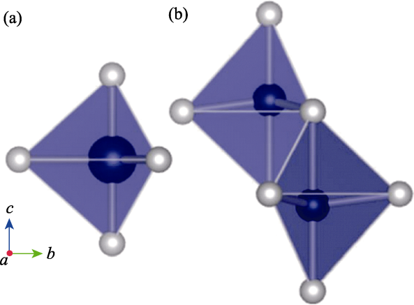
Fig. 2 Two types of trigonal bipyramid coordination in (RAO3)n(MO)m compounds[11] (a) Type I with D3h symmetry environment; (b) Type II with C3v symmetry environment
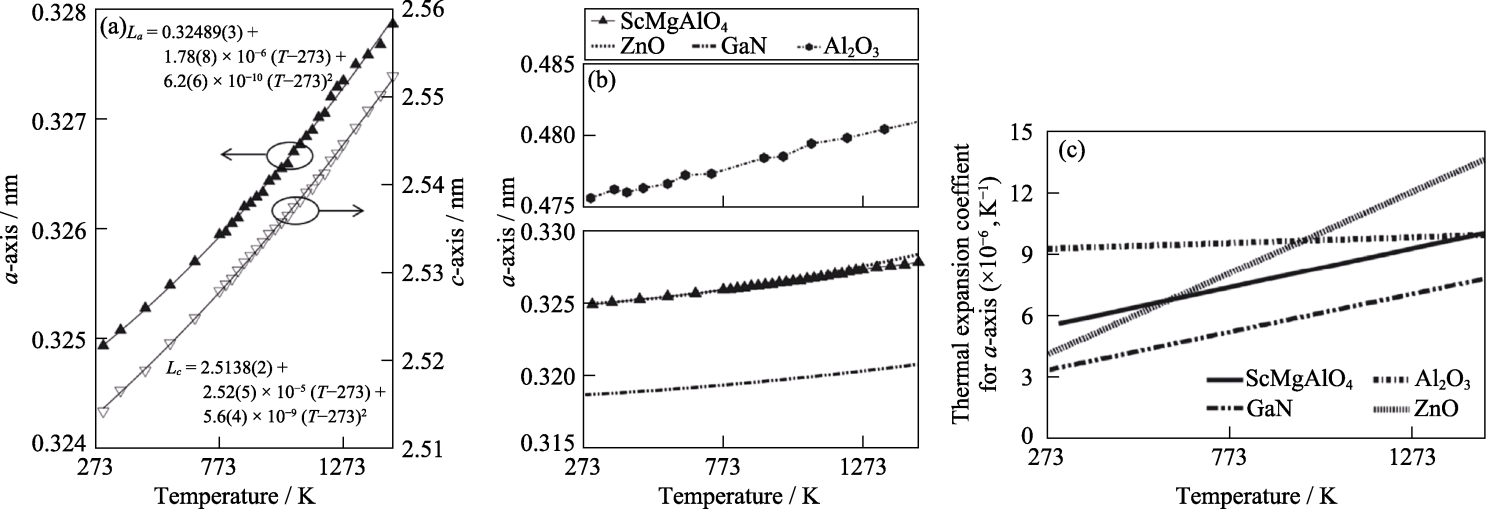
Fig. 4 Thermal properties of SCAM[37] (a) Cell parameters for SCAM as a function of temperature based on the high temperature XRD; (b, c) Length of a-axis (b) and the axial thermal expansion coefficient for a-axis (c) of SCAM in comparison to those of GaN, ZnO and Al2O3

Fig. 5 Optical properties of SCAM[9] (a) Transmittance spectrum; (b) PL spectrum under 200 nm excitation; (c) PLE spectrum monitoring at 300-500 nm emission bands of SCAM crystal; Inset in (c) focuses on ~250 nm band
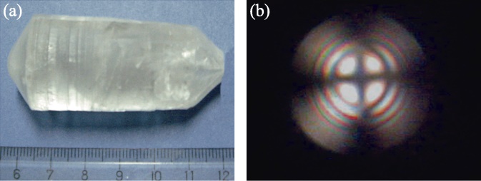
Fig. 7 SCAM single crystal grown by Cz method[38] (a) SCAM single crystal with the dimension of ϕ30 mm×59 mm grown by Cz method; (b) Interference photograph of (0001) SCAM wafer under the polarizing microscopy
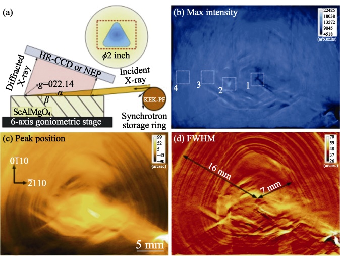
Fig. 9 Dislocation analysis of SCAM crystal grown by Fukuda laboratory[50] (a) Schematic diagram of the XRT test setup, and (b-d) reconstruct (b) maximum intensity map, (c) peak position map and (d) FWHM map using 201 XRT images
| Crystal | GaN | Sapphire | 6H-SiC | Si | GaAs | SCAM | |
|---|---|---|---|---|---|---|---|
| Space group | |||||||
| Lattice parameters | a=b=0.319 nm c=0.519 nm α=β=90° γ=120° | a=b=0.476 nm c=1.299 nm α=β=90° γ=120° | a=b=0.307 nm c=1.508 nm α=β=90° γ=120° | a=b=c=0.543 nm α=β=γ=90° | a=b=c=0.565 nm α=β=γ=90° | a=b=0.324 nm c=2.515 nm α=β=90° γ=120° | |
| Lattice mismatch, | GaN | 0 | 16%[ | 3.3%[ | 16%[ | 20%[ | 1.4%[ |
| ZnO | 2.2%[ | 18%[ | 5.8%[ | 16.6%[ | 22%[ | 0.09%[ | |
| Thermal expansion coefficient, α (~300 K)/(×10-6, K-1) | αa=3.43 αc=3.34[ | αa=7.5 αc=8.5[ | αa=3.2 αc=3.1[ | α=2.55[ | α=5.73[ | αa=5.59 αc=10.2[ | |
| Melting point/K | 2770[ | 2326[ | 3100[ | 1680[ | 1500[ | 2220[ | |
| Thermal conductivity, λ (~300 K)/(W·cm-1·K-1) | λc=2.2[ | λc=0.23[ | λc=4.3[ | λ=1.3[ | λ=0.55[ | λc=0.062[ | |
| Growth methods | HVPE MOCVD | Cz, KY, EFG | PVT | Cz | LEC, VB | Cz | |
| Cost | High | Medium | High | Low | Low | Low | |
Table 1 Common substrates for GaN and ZnO epitaxial layers
| Crystal | GaN | Sapphire | 6H-SiC | Si | GaAs | SCAM | |
|---|---|---|---|---|---|---|---|
| Space group | |||||||
| Lattice parameters | a=b=0.319 nm c=0.519 nm α=β=90° γ=120° | a=b=0.476 nm c=1.299 nm α=β=90° γ=120° | a=b=0.307 nm c=1.508 nm α=β=90° γ=120° | a=b=c=0.543 nm α=β=γ=90° | a=b=c=0.565 nm α=β=γ=90° | a=b=0.324 nm c=2.515 nm α=β=90° γ=120° | |
| Lattice mismatch, | GaN | 0 | 16%[ | 3.3%[ | 16%[ | 20%[ | 1.4%[ |
| ZnO | 2.2%[ | 18%[ | 5.8%[ | 16.6%[ | 22%[ | 0.09%[ | |
| Thermal expansion coefficient, α (~300 K)/(×10-6, K-1) | αa=3.43 αc=3.34[ | αa=7.5 αc=8.5[ | αa=3.2 αc=3.1[ | α=2.55[ | α=5.73[ | αa=5.59 αc=10.2[ | |
| Melting point/K | 2770[ | 2326[ | 3100[ | 1680[ | 1500[ | 2220[ | |
| Thermal conductivity, λ (~300 K)/(W·cm-1·K-1) | λc=2.2[ | λc=0.23[ | λc=4.3[ | λ=1.3[ | λ=0.55[ | λc=0.062[ | |
| Growth methods | HVPE MOCVD | Cz, KY, EFG | PVT | Cz | LEC, VB | Cz | |
| Cost | High | Medium | High | Low | Low | Low | |
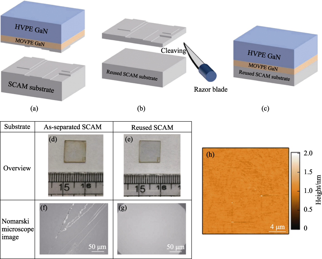
Fig. 11 SCAM substrate reuse process[58] (a) GaN film is naturally separated from SCAM substrate during the growth and cooling process of HVPE; (b) Separated SCAM substrate being cleaved with a razor blade to prepare the reusable SCAM substrate; (c) GaN film grown by MOVPE and HVPE being performed on the reusable SCAM substrate; (d, f) Photo and Nomarski microscope image of naturally separated SCAM substrate; (e, g) Photo and Nomarski microscope image of SCAM substrate cleaved with a razor blade; (h) AFM image of SCAM substrate cleaved with a razor blade
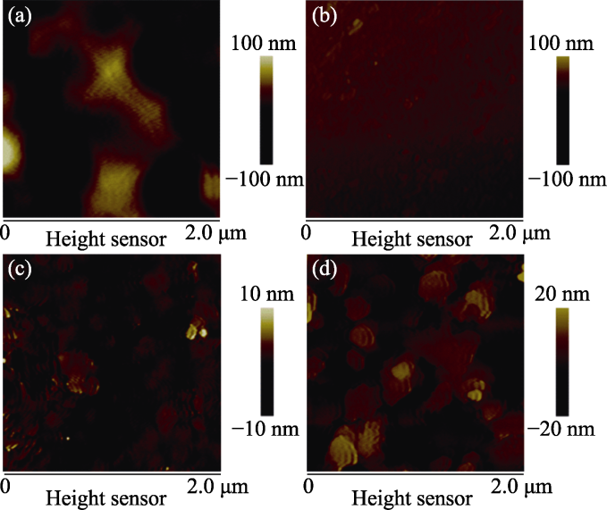
Fig. 12 AFM images of the ~300 nm-thick GaN epitaxial films grown on SCAM substrates with different laser repetition rates[85] (a) 10 Hz; (b) 20 Hz; (c) 30 Hz; (d) 40 Hz
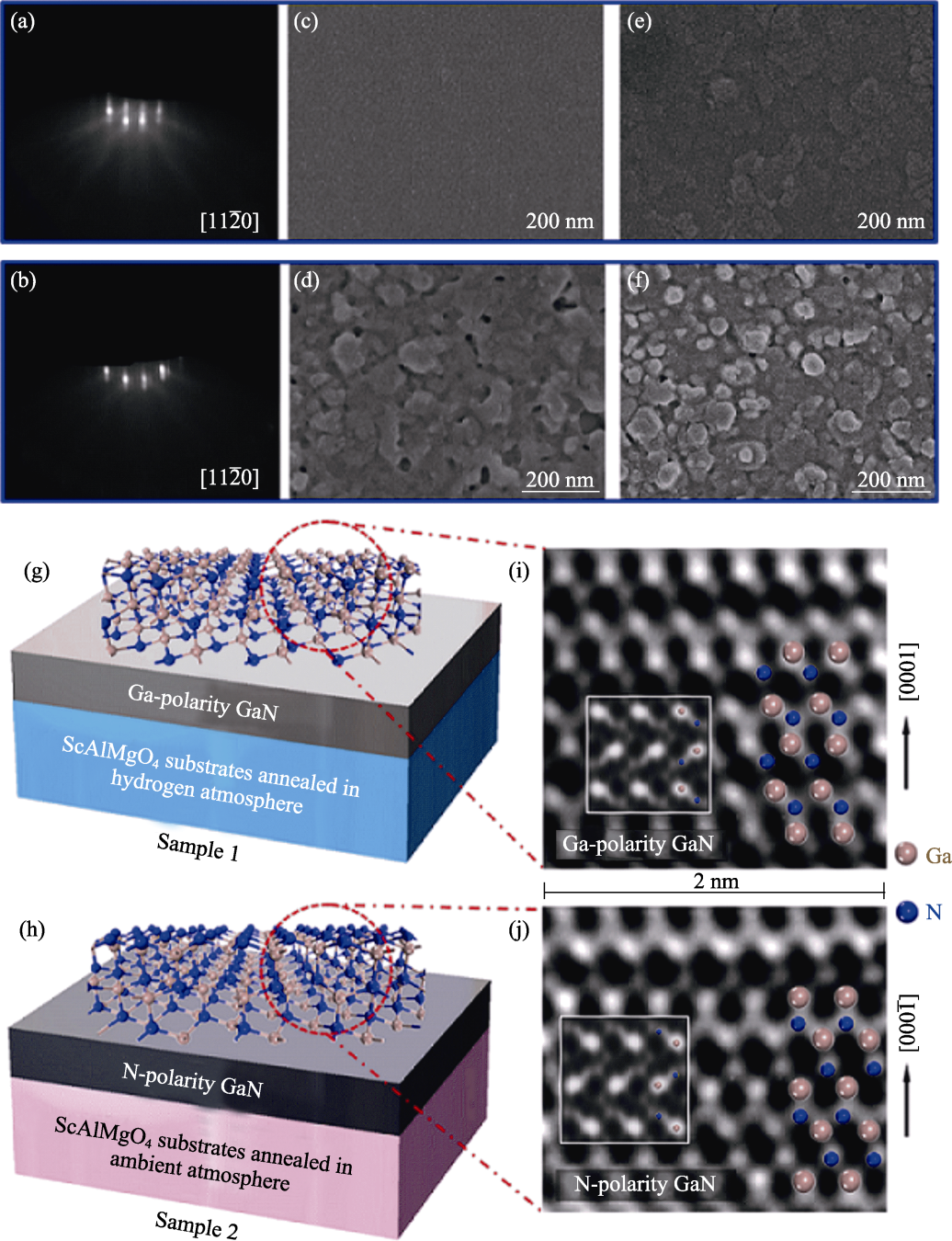
Fig. 13 GaN epitaxial films grown on SCAM substrate annealed under different atmospheres[86] (a, b) RHEED patterns for as-grown GaN epitaxial films on SCAM annealed in (a) hydrogen and (b) ambient atmosphere. (c, d) SEM images for as-grown GaN epitaxial films on SCAM annealed in (c) hydrogen and (d) ambient atmosphere; (e, f) Surfaces of GaN epitaxial films after molten KOH etching for (c) and (d), respectively; (g, h) Schematic structures of SCAM annealed in (g) hydrogen and (h) ambient atmosphere; (i, j) HAADF-STEM images and schematic illustrations of (i) Ga-polarity and (j) N-polarity GaN, where the bright spots in the HAADF images indicates Ga atoms and the dark ones indicates N atoms with insets showing the simulated micrograph
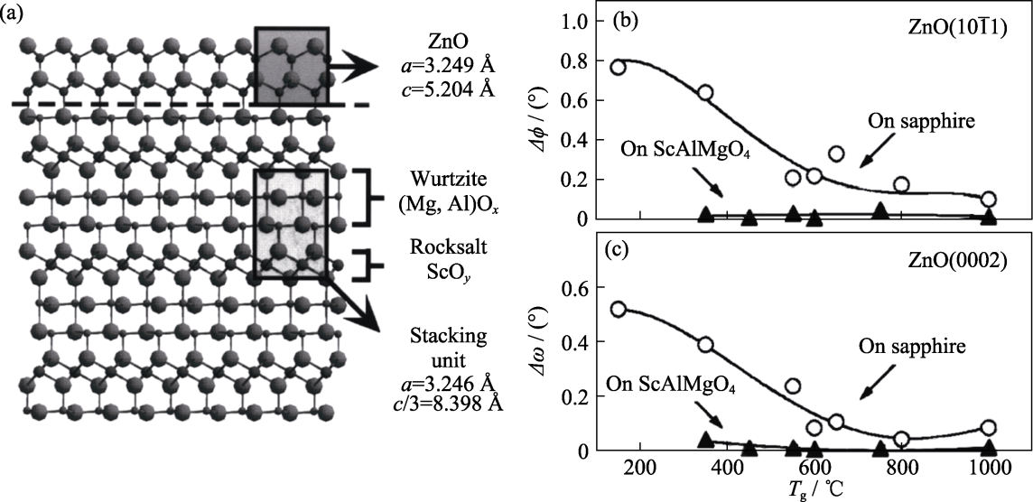
Fig. 15 ZnO films grown by laser-MBE on SCAM substrate[65] (a) Schematic illustration of the crystal structure of SCAM consisting of alternating layers of wurtzite AlMgO2.5 (0001) and rock salt ScO1.5 (111) layers; During epitaxy of ZnO, the wurtzite layer of SCAM is interconnected with the wurtzite layer of ZnO; (b, c) In-plane twisting (Δφ) and out-of-plane tilting (Δω) of epitaxial ZnO films on SCAM and sapphire substrates as a function of growth temperature; 1 Å=0.1 nm
| [1] |
ZHANG L, YU J, HAO X, et al. Influence of stress in GaN crystals grown by HVPE on MOCVD-GaN/6H-SiC substrate. Scientific Reports, 2014, 4: 4179.
DOI |
| [2] | ZHANG P M, WANG J F, CAI D M, et al. Progress on GaN single crystal substrate grown by hydride vapor phase epitaxy. Journal of Synthetic Crystals, 2020, 49(11): 1970. |
| [3] |
LEE W, PARK M, LEE W, et al. Characteristic comparison between GaN layer grown on c-plane cone shape patterned sapphire substrate and planar c-plane sapphire substrate by HVPE. Journal of Crystal Growth, 2018, 493: 8.
DOI URL |
| [4] |
LEE M, AHNC W, VUTK O, et al. First observation of electronic trap levels in freestanding GaN crystals extracted from Si substrates by hydride vapour phase epitaxy. Scientific Reports, 2019, 9(1): 7128.
DOI PMID |
| [5] |
TAMURA K, OHTOMO A, SAIKUSA K, et al. Epitaxial growth of ZnO films on lattice-matched ScAlMgO4 (0001) substrates. Journal of Crystal Growth, 2000, 214-215: 59.
DOI URL |
| [6] |
RAMIREZ P. Oxide electronics emerge. Science, 2007, 315: 1377.
DOI URL |
| [7] |
OBATA T, TAKAHASHI R, OHKUBO I, et al. Epitaxial ScAlMgO4 (0001) films grown on sapphire substrates by flux- mediated epitaxy. Applied Physics Letters, 2006, 89(19): 191910.
DOI URL |
| [8] |
KATASE T, NOMURA K, OHTA H, et al. Fabrication of ScAlMgO4 epitaxial thin films using ScGaO3(ZnO)m buffer layers and its application to lattice-matched buffer layer for ZnO epitaxial growth. Thin Solid Films, 2008, 516(17): 5842.
DOI URL |
| [9] |
YANAGIDA T, KOSHIMIZU M, KAWANO N, et al. Optical and scintillation properties of ScAlMgO4 crystal grown by the floating zone method. Materials Research Bulletin, 2017, 95: 409.
DOI URL |
| [10] |
NOBORU K, TAKAHIKO M, MASAKI N. Compounds which have InFeO3(ZnO)m-type structures (m= integer). Journal of Solid State Chemistry, 1989, 81: 70.
DOI URL |
| [11] |
GRAJCZYK R, SUBRAMANIAN M. Structure-property relationships of YbFe2O4- and Yb2Fe3O7-type layered oxides: a bird's eye view. Progress in Solid State Chemistry, 2015, 43(1/2): 37.
DOI URL |
| [12] |
AKEN B, MEETSMA A, PALSTRA T. Structural view of hexagonal non-perovskite AMnO3. 2001, DOI: 10.48550/arxiv.cond-mat/0106298.
DOI |
| [13] | VAN A, MEETSMA A, PALSTRA T. Hexagonal YMnO3. Acta Crystallographica Section C, 2001, 57(3): 230. |
| [14] |
MIZOGUCHI H, SLEIGHT A, SUBRAMANIAN M. New oxides showing an intense blue color based on Mn3+ in trigonal- bipyramidal coordination. Inorganic Chemistry, 2011, 50(1): 10.
DOI URL |
| [15] |
KATASE T, NOMURA K, OHTA H, et al. Large domain growth of GaN epitaxial films on lattice-matched buffer layer ScAlMgO4. Materials Science and Engineering: B, 2009, 161(1/2/3): 66.
DOI URL |
| [16] | SCHMITZ O, HORST K. Über eine neue klasse quarternärer oxide von typus MIIMIIIInO4. die lichtabsorption des 2-wertigen kupfers, nickels und kobalts sowie des 3-wertigen chroms. Journal of Inorganic and General Chemistry, 1965, 341(5/6): 252. |
| [17] |
KATO K, KAWADA I, KIMIZUKA N, et al. Die Kristallstruktur von YbFe2O4. Zeitschrift für Kristallographie-Crystalline Materials, 1975, 141(1-6): 314.
DOI URL |
| [18] |
GÉRARDIN R, ALEBOUYEH A, JEANNOT F, et al. Sur l'existence des oxydes rhomboe driques A(III)B(II)B(III)O4. Materials Research Bulletin, 1980, 15(5): 647.
DOI URL |
| [19] |
NOBORU K, AKIJI Y, HARUO O, et al. The stability of the phases in the Ln2O3-FeO-Fe2O3 systems which are stable at elevated temperatures (Ln: Lanthanide elements and Y). Journal of Solid State Chemistry, 1983, 49(1): 65.
DOI URL |
| [20] |
NESPOLO M, SATO A, OSAWA T, et al. Synthesis, crystal structure and charge distribution of InGaZnO4. X-ray diffraction study of 20 kB single crystal and 50 kB twin by reticular merohedry. Crystal Research and Technology, 2000, 35(2): 151.
DOI URL |
| [21] |
MURAT A, MEDVEDEVA J E. Electronic properties of layered multicomponent wide-band-gap oxides: a combinatorial approach. Physical Review B, 2012, 85(15): 155101.
DOI URL |
| [22] |
WALSH A, DA S, WEI S, et al. Nature of the band gap of In2O3 revealed by first-principles calculations and X-ray spectroscopy. Physical Review Letters, 2008, 100(16): 167402.
DOI URL |
| [23] |
WALSH A, DA F, WEI S. Origins of band-gap renormalization in degenerately doped semiconductors. Physical Review B, 2008, 78(7): 075211.
DOI URL |
| [24] |
KÖRBER C, KRISHNAKUMAR V, KLEIN A, et al. Electronic structure of In2O3 and Sn-doped In2O3 by hard X-ray photoemission spectroscopy. Physical Review B, 2010, 81(16): 165207.
DOI URL |
| [25] |
WALSH A, DA S, WEI S. Multi-component transparent conducting oxides: progress in materials modelling. Journal of Physics-Condensed Matter, 2011, 23(33): 334210.
DOI URL |
| [26] |
HUDA M, YAN Y, WALSH A, et al. Group-IIIA versus IIIB delafossites: electronic structure study. Physical Review B, 2009, 80(3): 035205.
DOI URL |
| [27] |
SCANLON D, WALSH A, MORGAN B, et al. Effect of Cr substitution on the electronic structure of CuAl1-xCrxO2. Physical Review B, 2009, 79(3): 035101.
DOI URL |
| [28] |
SCANLON D, WALSH A, WATSON G. Understanding the p-type conduction properties of the transparent conducting oxide CuBO2: a density functional theory analysis. Chemistry of Materials, 2009, 21(19): 4568.
DOI URL |
| [29] |
WALSH A, DA S, WEI S. Interplay between order and disorder in the high performance of amorphous transparent conducting oxides. Chemistry of Materials, 2009, 21(21): 5119.
DOI URL |
| [30] |
WALSH A, CATLOW C. Structure, stability and work functions of the low index surfaces of pure indium oxide and Sn-doped indium oxide (ITO) from density functional theory. Journal of Materials Chemistry, 2010, 20(46): 10438.
DOI URL |
| [31] |
TAMURA K, MAKINO T, TSUKAZAKI A, et al. Donor-acceptor pair luminescence in nitrogen-doped ZnO films grown on lattice- matched ScAlMgO4 (0001) substrates. Solid State Communications, 2003, 127(4): 265.
DOI URL |
| [32] |
MEDVEDEVA J, HETTIARACHCHI C. Tuning the properties of complex transparent conducting oxides: role of crystal symmetry, chemical composition, and carrier generation. Physical Review B, 2010, 81(12): 125116.
DOI URL |
| [33] |
NOBORU K, TAKAHIKOM. Spinel, YbFe2O4, and Yb2Fe3O7 types of structures for compounds in the In2O3 and Sc2O3-A2O3-BO systems [A: Fe, Ga, or Al; B: Mg, Mn, Fe, Ni, Cu, or Zn] at temperatures over 1000 ℃. Journal of Solid State Chemistry, 1985, 60(3): 382.
DOI URL |
| [34] |
BYLANDER D, KLEINMAN L. Good semiconductor band gaps with a modified local-density approximation. Physical Review B, 1990, 41(11): 7868.
PMID |
| [35] | HELLMAN E, BRANDLE C, SCHNEEMEYER L, et al. ScAlMgO4: an oxide substrate for GaN epitaxy. MRS Internet Journal of Nitride Semiconductor Research, 1996, 1: U3. |
| [36] |
IWANAGA H, KUNISHIGE A, TAKEUCHI S. Anisotropic thermal expansion in wurtzite-type crystals. Journal of Materials Science, 2000, 35: 2451.
DOI URL |
| [37] |
SIMURA R, SUGIYAMA K, NAKATSUKA A, et al. High-temperature thermal expansion of ScAlMgO4 for substrate application of GaN and ZnO epitaxial growth. Japanese Journal of Applied Physics, 2016, 55(9): 099201.
DOI |
| [38] |
TANG H, XU J, DONG Y, et al. Study on growth and characterization of ScAlMgO4 substrate crystal. Journal of Alloys and Compounds, 2009, 471(1/2): L43.
DOI URL |
| [39] |
DE HAAS J, DORENBOS P. Advances in yield calibration of scintillators. IEEE Transactions on Nuclear Science, 2008, 55(3): 1086.
DOI URL |
| [40] |
ABRAHAMS S, MARSH P, BRANDLE C. Laser and phosphor host La1-xMgAl11+xO19 (x=0.050): crystal structure at 295 K. The Journal of Chemical Physics, 1986, 86(5): 4221.
DOI URL |
| [41] | CHAUD X, MESLIN S, NOUDEM J, et al. Isothermal growth of large YBaCuO single domains through an artificial array of holes. Journal of Crystal Growth, 2005, 275(1/2): 855. |
| [42] | HANSKARL B. Über Oxoscandate. II. Zur Kenntnis des MgSc2O4. Journal of Inorganic and General Chemistry, 1966, 343(3/4): 113. |
| [43] |
NANCY R. High pressure study of ScAlO3 perovskite. Physics and Chemistry of Minerals, 1998, 25: 597.
DOI URL |
| [44] |
ZAWRAH M, HAMAAD H, MEKY S. Synthesis and characterization of nano MgAl2O4 spinel by the co-precipitated method. Ceramics International, 2007, 33(6): 969.
DOI URL |
| [45] | TANG H, DONG Y, XU J, et al. Study on the growth of lattice-matched ScAlMgO4 substrate for GaN and ZnO based film epitaxy. Journal of Synthetic Crystals, 2007, 36(3): 612. |
| [46] |
NOBORU K, TAKAHIKO M, YOSHIO M, et al. Homologous compounds, InFeO3(ZnO)m (m=1-9). Journal of Solid State Chemistry, 1988, 74(1): 98.
DOI URL |
| [47] | TANG H, DONG Y, XU J, et al. Growth defects of ScAlMgO4 crystal. Journal of the Chinese Ceramic Society, 2008, 36(5): 689. |
| [48] |
FUKUDA T, SHIRAISHI Y, NANTO T, et al. Growth of bulk single crystal ScAlMgO4 boules and GaN films on ScAlMgO4 substrates for GaN-based optical devices, high-power and high- frequency transistors. Journal of Crystal Growth, 2021, 574: 126286.
DOI URL |
| [49] | ISHIJI K, FUJII T, ARAKI T, et al. Observation of defect structure in ScAlMgO4 crystal using X-ray topography. Journal of Crystal Growth, 2022, 580: 136477. |
| [50] |
YAO Y, HIRANO K, YAMAGUCHI H, et al. A synchrotron X-ray topography study of crystallographic defects in ScAlMgO4 single crystals. Journal of Alloys and Compounds, 2022, 896: 163025.
DOI URL |
| [51] |
KARCH K, WAGNER M, BECHSTEDT F. Ab initio study of structural, dielectric, and dynamical properties of GaN. Physical Review B, 1998, 57(12): 7043.
DOI URL |
| [52] |
ZOU J, KOTCHETKOV D, BALANDIN A, et al. Thermal conductivity of GaN films: effects of impurities and dislocations. Journal of Applied Physics, 2002, 92(5): 2534.
DOI URL |
| [53] |
STEPHEN P, FAN R. GaN electronics. Advanced Materials, 2000, 12(21): 1571.
DOI URL |
| [54] |
LIU L, EDGAR J. Substrates for gallium nitride epitaxy. Materials Science and Engineering R, 2002, 37: 61.
DOI URL |
| [55] |
WANG W, YANG W, WANG H, et al. Epitaxial growth of GaN films on unconventional oxide substrates. Journal of Materials Chemistry C, 2014, 2(44): 9342.
DOI URL |
| [56] |
WANG W, YAN T, YANG W, et al. Effect of growth temperature on the properties of GaN epitaxial films grown on magnesium aluminate scandium oxide substrates by pulsed laser deposition. Materials Letters, 2016, 183: 382.
DOI URL |
| [57] |
ERRANDONEA D, KUMAR R S, RUIZ-FUERTES J, et al. High-pressure study of substrate material ScAlMgO4. Physical Review B, 2011, 83(14): 144104.
DOI URL |
| [58] |
OHNISHI K, KUBOYA S, TANIKAWA T, et al. Reuse of ScAlMgO4 substrates utilized for halide vapor phase epitaxy of GaN. Japanese Journal of Applied Physics, 2019, 58(C): SC1023.
DOI |
| [59] |
FUKUI T, SAKAGUCHI T, MATSUDA Y, et al. Metalorganic vapor phase epitaxy of GaN on 2 inch ScAlMgO4 (0001) substrates. Japanese Journal of Applied Physics, 2022, 61(9): 090904.
DOI |
| [60] |
UETA A, OHNO H, YANAGITA N, et al. High quality nitride semiconductors grown on novel ScAlMgO4 substrates and their light emitting diodes. Japanese Journal of Applied Physics, 2019, 58(C): SC1041.
DOI URL |
| [61] |
WILLIAM M, JACQUES P. GaN growth on sapphire. Journal of Crystal Growth. 1997, 178: 168.
DOI URL |
| [62] |
PAL S, JACOB C. Silicon-a new substrate for GaN growth. Bulletin of Materials Science, 2004, 27(6): 501.
DOI URL |
| [63] |
DING S A, BARMAN S R, HORN K, et al. Valence band discontinuity at a cubic GaN/GaAs heterojunction measured by synchrotron-radiation photoemission spectroscopy. Applied Physics Letters, 1997, 70(18): 2407.
DOI URL |
| [64] |
FAUGIER J, LAZAR F, MARICHY C, et al. Influence of the lattice mismatch on the atomic ordering of ZnO grown by atomic layer deposition onto single crystal surfaces with variable mismatch (InP, GaAs, GaN, SiC). Condensed Matter, 2017, 2(1): 3.
DOI URL |
| [65] |
OHTOMO A, TAMURA K, SAIKUSA K. Single crystalline ZnO films grown on lattice-matched ScAlMgO4(0001) substrates. Applied Physics Letters, 1999, 75(17): 2635.
DOI URL |
| [66] |
HASSAN J J, MAHDI M A, RAMIZY A, et al. Fabrication and characterization of ZnO nanorods/p-6H-SiC heterojunction LED by microwave-assisted chemical bath deposition. Superlattices and Microstructures, 2013, 53: 31.
DOI URL |
| [67] |
ZHU J, LIN B, SUN X, et al. Heteroepitaxy of ZnO film on Si(111) substrate using a 3C-SiC buffer layer. Thin Solid Films, 2005, 478(1/2): 218.
DOI URL |
| [68] |
DEHM G, INKSON B, WAGNER T. Growth and microstructural stability of epitaxial Al films on (0001) α-Al2O3 substrates. Acta Materialia, 2002, 50: 5021.
DOI URL |
| [69] |
STOCKMEIER M, SAKWE S A, HENS P, et al. Thermal expansion coefficients of 6H silicon carbide. Materials Science Forum, 2008, 600-603: 517.
DOI URL |
| [70] |
MIDDELMANN T, WALKOV A, BARTL G, et al. Thermal expansion coefficient of single-crystal silicon from 7 K to 293 K. Physical Review B, 2015, 92(17): 174113.
DOI URL |
| [71] |
SOMA T, SATOH J, MATSUO H. Thermal expansion coefficient of GaAs and InP. Solid State Communications, 1982, 42(12): 889.
DOI URL |
| [72] | KURLOV V. Sapphire:Properties, Growth, and Applications. Encyclopedia of Materials:Science and Technology, Elsevier Science Ltd., 2001: 8259-8264. |
| [73] |
LIU Z, MASUDA A, KONDO M. Investigation on the crystal growth process of spherical Si single crystals by melting. Journal of Crystal Growth, 2009, 311(16): 4116.
DOI URL |
| [74] |
KAKIMOTO K, HIBIYA T. Temperature dependence of viscosity of molten GaAs by an oscillating cup method. Applied Physics Letters, 1987, 50(18): 1249.
DOI URL |
| [75] |
ZHENG Q, LI C, RAI A, et al. Thermal conductivity of GaN, 71GaN, and SiC from 150 K to 850 K. Physical Review Materials, 2019, 3(1): 014601.
DOI URL |
| [76] |
SHIBATA H, WASEDA Y, OHTA H, et al. High thermal conductivity of gallium nitride (GaN) crystals grown by HVPE process. Materials Transactions, 2007, 48(10): 2782.
DOI URL |
| [77] |
GLASSBRENNER C, SLACK G. Thermal conductivity of silicon and Germanium from 3 K to the melting point. Physical Review, 1964, 134(4A): A1058.
DOI URL |
| [78] |
CARLSON R, SLACK G, SILVERMAN S. Thermal conductivity of GaAs and GaAs1-xPx laser semiconductors. Journal of Applied Physics, 1965, 36(2): 505.
DOI URL |
| [79] |
LI G, WANG W, YANG W, et al. Epitaxial growth of group III- nitride films by pulsed laser deposition and their use in the development of LED devices. Surface Science Reports, 2015, 70: 380.
DOI URL |
| [80] |
WANG W, YANG W, LI G. Quality-enhanced GaN epitaxial films grown on (La, Sr)(Al, Ta)O3 substrates by pulsed laser deposition. Materials Letters, 2016, 168: 52.
DOI URL |
| [81] | IWABUCHI T, KUBOYA S, TANIKAWA T, et al. Ga-polar GaN film grown by MOVPE on cleaved ScAlMgO4(0001) substrate with millimeter-scale wide terraces. Physica Status Solidi A, 2017, 214(9): 1600754. |
| [82] |
FLORIDUZ A, MATIOLI E. Direct high-temperature growth of single-crystalline GaN on ScAlMgO4 substrates by metalorganic chemical vapor deposition. Japanese Journal of Applied Physics, 2022, 61(4): 048002.
DOI |
| [83] |
KIM T, MATSUKI N, OHTA J, et al. Epitaxial growth of AlN on single-crystal Ni(111) substrates. Applied Physics Letters, 2006, 88(12): 121916.
DOI URL |
| [84] |
CAI H, LIANG P, HÜBNER R, et al. Composition and bandgap control of AlxGa1-xN films synthesized by plasma-assisted pulsed laser deposition. Journal of Materials Chemistry C, 2015, 3(20): 5307.
DOI URL |
| [85] |
WANG W, YAN T, YANG W, et al. Epitaxial growth of GaN films on lattice-matched ScAlMgO4 substrates. CrystEngComm, 2016, 18(25): 4688.
DOI URL |
| [86] |
ZHENG Y, WANG W, LI X, et al. Polarity-controlled GaN epitaxial films achieved via controlling the annealing process of ScAlMgO4 substrates and the corresponding thermodynamic mechanisms. The Journal of Physical Chemistry C, 2018, 122(28): 16161.
DOI URL |
| [87] |
BORYSIEWICZ M. ZnO as a functional material: a review. Crystals, 2019, 9(10): 505.
DOI URL |
| [88] |
KOZUKA Y, TSUKAZAKI A, KAWASAKI M. Challenges and opportunities of ZnO-related single crystalline heterostructures. Applied Physics Reviews, 2014, 1(1): 011303.
DOI URL |
| [89] |
HALLIBURTON L, GILES N, GARCES N, et al. Production of native donors in ZnO by annealing at high temperature in Zn vapor. Applied Physics Letters, 2005, 87(17): 172108.
DOI URL |
| [90] |
KIM K, NIKI S, OH J, et al. High electron concentration and mobility in Al-doped n-ZnO epilayer achieved via dopant activation using rapid-thermal annealing. Journal of Applied Physics, 2005, 97(6): 066103.
DOI URL |
| [91] |
MAKINO T, SEGAWA Y, TSUKAZAKI A, et al. Electron transport in ZnO thin films. Applied Physics Letters, 2005, 87(2): 022101.
DOI URL |
| [92] | LOOK D. Recent advances in ZnO materials and devices. Materials Science and Engineering, 2001, B80: 383. |
| [93] |
LOOK D, CLAFLIN B. P-type doping and devices based on ZnO. Physica Status Solidi B, 2004, 241(3): 624.
DOI URL |
| [94] |
LOOK D, CLAFLIN B, ALIVOV Y I, et al. The future of ZnO light emitters. Physica Status Solidi A, 2004, 201(10): 2203.
DOI URL |
| [95] |
NEAL J, GILES N, YANG X, et al. Evaluation of melt-grown, ZnO single crystals for use as alpha-particle detectors. IEEE Transactions on Nuclear Science, 2008, 55(3): 1397.
DOI URL |
| [96] |
TSUKAZAKI A, OHTOMO A, ONUMA T, et al. Repeated temperature modulation epitaxy for p-type doping and light-emitting diode based on ZnO. Nature Materials, 2004, 4(1): 42.
DOI |
| [97] |
WEN M C, YAN T, CHANG L, et al. Achieving high MgO content in wurtzite ZnO epilayer grown on ScAlMgO4 substrate. Journal of Crystal Growth, 2017, 477: 174.
DOI URL |
| [98] |
TRINKLER L, AULIKA I, KRIEKE G, et al. Characterization of wurtzite Zn1-xMgxO epilayers grown on ScAlMgO4 substrate by methods of optical spectroscopy. Journal of Alloys and Compounds, 2022, 912: 165178.
DOI URL |
| [99] |
TSUKAZAKI A, SAITO H, TAMURA K, et al. Systematic examination of carrier polarity in composition spread ZnO thin films codoped with Ga and N. Applied Physics Letters, 2002, 81(2): 235.
DOI URL |
| [100] |
MASASHI O, HIROMITSU K, TOSHINOBU Y. Sol-Gel preparation of ZnO films with extremely preferred orientation along (002) plane from zinc acetate solution. Thin Solid Films, 1997, 306: 78.
DOI URL |
| [101] |
YUTAKA O, HISAO S, TOSHIMASA T, et al. Microstructure of TiO2 and ZnO films fabricated by the Sol-Gel method. Journal of the American Ceramic Society, 1996, 79: 825.
DOI URL |
| [102] |
WESSLER B, STEINECKER A, MADER W. Epitaxial growth of ZnO thin films on ScAlMgO4 (0001) by chemical solution deposition. Journal of Crystal Growth, 2002, 242: 283.
DOI URL |
| [103] |
KATASE T, NOMURA K, OHTA H, et al. Fabrication of atomically flat ScAlMgO4 epitaxial buffer layer and low- temperature growth of high-mobility ZnO films. Crystal Growth & Design, 2010, 10(3): 1084.
DOI URL |
| [1] | ZHU Wenjie, TANG Lu, LU Jichang, LIU Jiangping, LUO Yongming. Research Progress on Catalytic Oxidation of Volatile Organic Compounds by Perovskite Oxides [J]. Journal of Inorganic Materials, 2025, 40(7): 735-746. |
| [2] | HU Zhichao, YANG Hongyu, YANG Hongcheng, SUN Chengli, YANG Jun, LI Enzhu. Usage of the P-V-L Bond Theory in Regulating Properties of Microwave Dielectric Ceramics [J]. Journal of Inorganic Materials, 2025, 40(6): 609-626. |
| [3] | WU Qiong, SHEN Binglin, ZHANG Maohua, YAO Fangzhou, XING Zhipeng, WANG Ke. Research Progress on Lead-based Textured Piezoelectric Ceramics [J]. Journal of Inorganic Materials, 2025, 40(6): 563-574. |
| [4] | ZHANG Bihui, LIU Xiaoqiang, CHEN Xiangming. Recent Progress of Hybrid Improper Ferroelectrics with Ruddlesden-Popper Structure [J]. Journal of Inorganic Materials, 2025, 40(6): 587-608. |
| [5] | WU Jie, YANG Shuai, WANG Mingwen, LI Jinglei, LI Chunchun, LI Fei. Textured PT-based Piezoelectric Ceramics: Development, Status and Challenge [J]. Journal of Inorganic Materials, 2025, 40(6): 575-586. |
| [6] | JIANG Kun, LI Letian, ZHENG Mupeng, HU Yongming, PAN Qinxue, WU Chaofeng, WANG Ke. Research Progress on Low-temperature Sintering of PZT Ceramics [J]. Journal of Inorganic Materials, 2025, 40(6): 627-638. |
| [7] | TIAN Ruizhi, LAN Zhengyi, YIN Jie, HAO Nanjing, CHEN Hangrong, MA Ming. Microfluidic Technology Based Synthesis of Inorganic Nano-biomaterials: Principles and Progress [J]. Journal of Inorganic Materials, 2025, 40(4): 337-347. |
| [8] | ZHANG Jiguo, WU Tian, ZHAO Xu, YANG Fan, XIA Tian, SUN Shien. Improvement of Cycling Stability of Cathode Materials and Industrialization Process for Sodium-ion Batteries [J]. Journal of Inorganic Materials, 2025, 40(4): 348-362. |
| [9] | YIN Jie, GENG Jiayi, WANG Kanglong, CHEN Zhongming, LIU Xuejian, HUANG Zhengren. Recent Advances in 3D Printing and Densification of SiC Ceramics [J]. Journal of Inorganic Materials, 2025, 40(3): 245-255. |
| [10] | CHEN Guangchang, DUAN Xiaoming, ZHU Jinrong, GONG Qing, CAI Delong, LI Yuhang, YANG Donglei, CHEN Biao, LI Xinmin, DENG Xudong, YU Jin, LIU Boya, HE Peigang, JIA Dechang, ZHOU Yu. Advanced Ceramic Materials in Helicopter Special Structures: Research Progress and Application Prospect [J]. Journal of Inorganic Materials, 2025, 40(3): 225-244. |
| [11] | FAN Xiaobo, ZU Mei, YANG Xiangfei, SONG Ce, CHEN Chen, WANG Zi, LUO Wenhua, CHENG Haifeng. Research Progress on Proton-regulated Electrochemical Ionic Synapses [J]. Journal of Inorganic Materials, 2025, 40(3): 256-270. |
| [12] | HAIREGU Tuxun, GUO Le, DING Jiayi, ZHOU Jiaqi, ZHANG Xueliang, NUERNISHA Alifu. Research Progress of Optical Bioimaging Technology Assisted by Upconversion Fluorescence Probes in Tumor Imaging [J]. Journal of Inorganic Materials, 2025, 40(2): 145-158. |
| [13] | SUN Shujuan, ZHENG Nannan, PAN Haokun, MA Meng, CHEN Jun, HUANG Xiubing. Research Progress on Preparation Methods of Single-atom Catalysts [J]. Journal of Inorganic Materials, 2025, 40(2): 113-127. |
| [14] | TAO Guilong, ZHI Guowei, LUO Tianyou, OUYANG Peidong, YI Xinyan, LI Guoqiang. Progress on Key Technologies of Cavity-structured Thin Film Bulk Acoustic Wave Filter [J]. Journal of Inorganic Materials, 2025, 40(2): 128-144. |
| [15] | ZHOU Fan, TIAN Zhilin, LI Bin. Research Progress on Carbide Ultra-high Temperature Ceramic Anti-ablation Coatings for Thermal Protection System [J]. Journal of Inorganic Materials, 2025, 40(1): 1-16. |
| Viewed | ||||||
|
Full text |
|
|||||
|
Abstract |
|
|||||