Journal of Inorganic Materials ›› 2024, Vol. 39 ›› Issue (4): 416-422.DOI: 10.15541/jim20230392
Special Issue: 【AI4材料】Al4材料(202512); 【信息功能】功能晶体(202512)
• RESEARCH ARTICLE • Previous Articles Next Articles
WANG Weihua1( ), ZHANG Leining2, DING Feng3(), DAI Bing4(), HAN Jiecai4, ZHU Jiaqi4, JIA Yi1, Yang Yu5
Received:2023-08-30
Revised:2023-11-06
Published:2024-04-20
Online:2023-11-28
Contact:
DING Feng, professor. E-mail: f.ding@siat.ac.cn;About author:WANG Weihua (1992-), male, PhD. E-mail: weihuawang2011@163.com
Supported by:CLC Number:
WANG Weihua, ZHANG Leining, DING Feng, DAI Bing, HAN Jiecai, ZHU Jiaqi, JIA Yi, Yang Yu. Heteroepitaxial Diamond Nucleation and Growth on Iridium: First-principle Calculation[J]. Journal of Inorganic Materials, 2024, 39(4): 416-422.
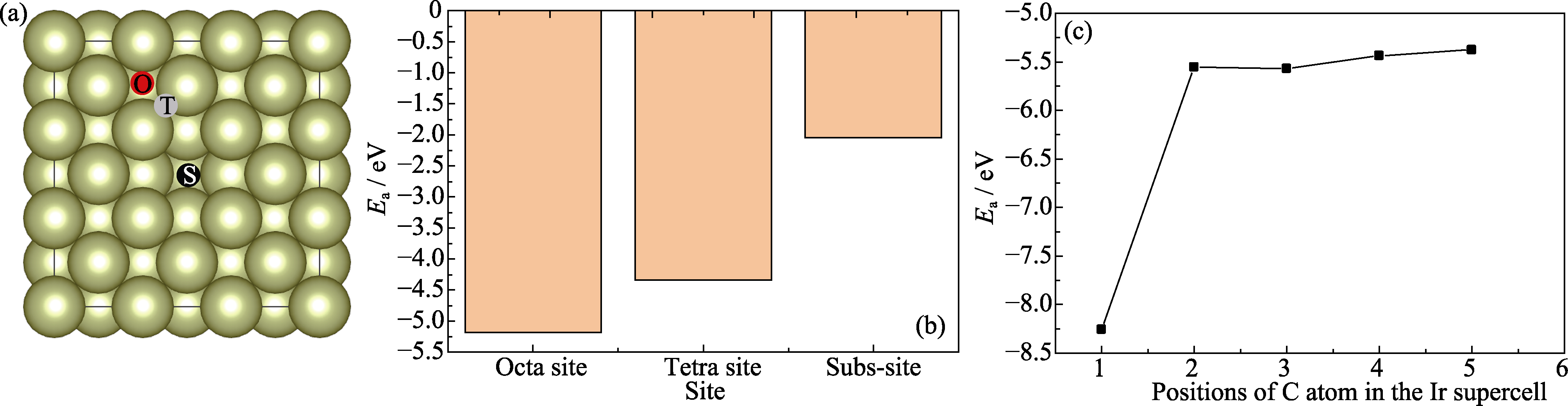
Fig. 1 Adsorption modes and behaviors of C atom on Ir substrate (a) Adsorption modes of C atom in octa-site (O), tetra-site (T) and subs-site (S) of the surface; (b) Adsorption energy when one C atom is adsorbed on different sites of Ir substrate; (c) Adsorption energy variation of C atoms adsorbed on different depths from Ir (001) surface
| Ion rate | 0.005 nm/fs | 0.011 nm/fs | 0.019 nm/fs | 0.025 nm/fs | 0.030 nm/fs | 0.035 nm/fs | ||||||
|---|---|---|---|---|---|---|---|---|---|---|---|---|
| Number Step | C atom | sp3-C atom | C atom | sp3-C atom | C atom | sp3-C atom | C atom | sp3-C atom | C atom | sp3-C atom | C atom | sp3-C atom |
| 2500 | 4 | 0 | 4 | 0 | 6 | 0 | 6 | 0 | 6 | 0 | 6 | 0 |
| 5000 | 9 | 0 | 7 | 1 | 9 | 0 | 11 | 0 | 11 | 0 | 11 | 0 |
| 7500 | 6 | 0 | 13 | 1 | 15 | 0 | 15 | 0 | 17 | 0 | 17 | 1 |
| 10000 | - | 16 | 3 | 21 | 1 | 17 | 2 | 20 | 2 | 23 | 1 | |
| 12500 | 21 | 4 | 22 | 1 | 18 | 2 | 23 | 0 | 26 | 1 | ||
| 15000 | 17 | 5 | - | - | - | - | - | |||||
Table 1 Carbon atom number and sp3-bonded carbon number in the a-C:H layer after the CH3+ ion bombardment with different rates
| Ion rate | 0.005 nm/fs | 0.011 nm/fs | 0.019 nm/fs | 0.025 nm/fs | 0.030 nm/fs | 0.035 nm/fs | ||||||
|---|---|---|---|---|---|---|---|---|---|---|---|---|
| Number Step | C atom | sp3-C atom | C atom | sp3-C atom | C atom | sp3-C atom | C atom | sp3-C atom | C atom | sp3-C atom | C atom | sp3-C atom |
| 2500 | 4 | 0 | 4 | 0 | 6 | 0 | 6 | 0 | 6 | 0 | 6 | 0 |
| 5000 | 9 | 0 | 7 | 1 | 9 | 0 | 11 | 0 | 11 | 0 | 11 | 0 |
| 7500 | 6 | 0 | 13 | 1 | 15 | 0 | 15 | 0 | 17 | 0 | 17 | 1 |
| 10000 | - | 16 | 3 | 21 | 1 | 17 | 2 | 20 | 2 | 23 | 1 | |
| 12500 | 21 | 4 | 22 | 1 | 18 | 2 | 23 | 0 | 26 | 1 | ||
| 15000 | 17 | 5 | - | - | - | - | - | |||||
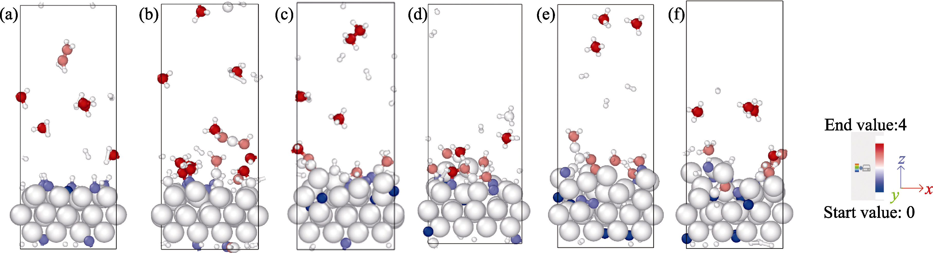
Fig. 2 Bonding types of C atoms after the CH3+ ion bombardment with different ion rates (a) 0.005 nm/fs; (b) 0.011 nm/fs; (c) 0.019 nm/fs; (d) 0.025 nm/fs; (e) 0.030 nm/fs; (f) 0.035 nm/fs Atoms with the atomic size from large to small representing Ir, C and H, and C atom with the color from blue to red representing the bonding number of C atom from 0 to 4. Colorful figures are available on website
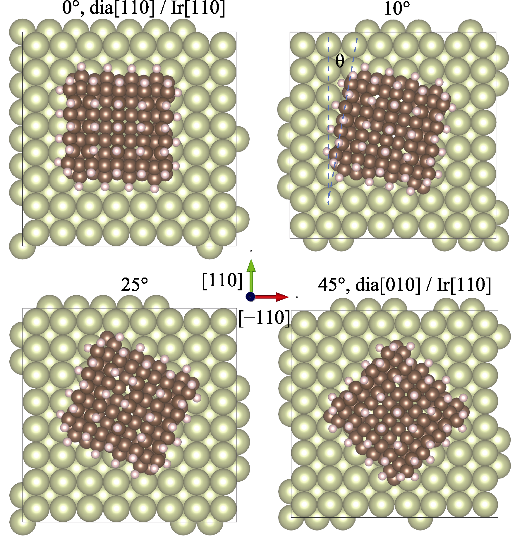
Fig. 3 Structure of cluster model of diamond (001) and Ir (001) surface as a function of the alignment angle θ=0°, 10°, 25° and 45° When θ are 0° and 45°, the in-plane orientation relationships are diamond(001)[010]//Ir(001)[010] and diamond(001)[110]//Ir(001)[010], respectively

Fig. 4 Binding energy for the diamond-Ir system as a function of the alignment angle θ (a), and SEM surface morphology of diamond grains on Ir (001) surface (b) No.1-4 represent grains with different sizes and shapes
| [1] | PARK K, LEE H-P, VAN DUREN J K J, et al. Single crystal diamond: an ultimate semiconductor. Chicago: Office of Science, U.S. Department of Energy, 2020. |
| [2] |
DANG C, CHOU J P, DAI B, et al. Achieving large uniform tensile elasticity in microfabricated diamond. Science, 2021, 371(6524): 76.
DOI PMID |
| [3] |
ALHASANI R, YABE T, IYAMA Y, et al. An enhanced two-dimensional hole gas (2DHG) C-H diamond with positive surface charge model for advanced normally-off MOSFET devices. Scientific Reports, 2022, 12: 4203.
DOI PMID |
| [4] |
LIU B, BI T, FU Y, et al. MOSFETs on (110) C-H diamond: ALD Al2O3/diamond interface analysis and high performance normally- OFF operation realization. IEEE Transactions on Electron Devices, 2022, 69(3): 949.
DOI URL |
| [5] |
BERDERMANN E, AFANACIEV K, CIOBANU M, et al. Progress in detector properties of heteroepitaxial diamond grown by chemical vapor deposition on Ir/YSZ/Si (001) wafers. Diamond and Related Materials, 2019, 97: 107420.
DOI URL |
| [6] |
LIAO M. Progress in semiconductor diamond photodetectors and MEMS sensors. Functional Diamond, 2021, 1(1): 29.
DOI URL |
| [7] |
SHIMAOKA T, KOIZUMI S J H, et al. Recent progress in diamond radiation detectors. Functional Diamond, 2021, 1(1): 205.
DOI URL |
| [8] |
ARNAULT J C, LEE K H, DELCHEVALRIE J, et al. Epitaxial diamond on Ir/SrTiO3/Si (001): from sequential material characterizations to fabrication of lateral schottky diodes. Diamond and Related Materials, 2020, 105: 107768.
DOI URL |
| [9] |
ACHARD J, JACQUES V, TALLAIRE A. Chemical vapour deposition diamond single crystals with nitrogen-vacancy centres: a review of material synthesis and technology for quantum sensing applications. Journal of Physics D: Applied Physics, 2020, 53(31): 313001.
DOI URL |
| [10] |
HO K O, SHEN Y, PANG Y Y, et al. Diamond quantum sensors: from physics to applications on condensed matter research. Functional Diamond, 2021, 1(1): 160.
DOI URL |
| [11] |
SANG L. Diamond as the heat spreader for the thermal dissipation of GaN-based electronic devices. Functional Diamond, 2021, 1(1): 174.
DOI URL |
| [12] |
YANG Q, ZHAO J, HUANG Y, et al. A diamond made microchannel heat sink for high-density heat flux dissipation. Applied Thermal Engineering, 2019, 158: 113804.
DOI URL |
| [13] |
LU W, LI J, MIAO J, et al. Application of high-thermal- conductivity diamond for space phased array antenna. Functional Diamond, 2021, 1(1): 189.
DOI URL |
| [14] |
GEIS M W, SMITH H I, ARGOITIA A, et al. Large‐area mosaic diamond films approaching single-crystal quality. Applied Physics Letters, 1991, 58(22): 2485.
DOI URL |
| [15] |
YAMADA H, CHAYAHARA A, MOKUNO Y, et al. A 2-in. mosaic wafer made of a single-crystal diamond. Applied Physics Letters, 2014, 104(10): 102110.
DOI URL |
| [16] |
YELISSEYEV A P, ZHIMULEV E I, KARPOVICH Z A, et al. Characterization of the nitrogen state in HPHT diamonds grown in an Fe-C melt with a low sulfur addition. CrystEngComm, 2022, 24: 4408.
DOI URL |
| [17] |
CHERNYKH S V, CHERNYKH A V, TARELKIN S A, et al. High-pressure high-temperature single-crystal diamond type IIa characterization for particle detectors. Physica Status Solidi (a), 2020, 217(8): 1900888.
DOI URL |
| [18] |
CHARRIS A, NAD S, ASMUSSEN J. Exploring constant substrate temperature and constant high pressure SCD growth using variable pocket holder depths. Diamond and Related Materials, 2017, 76: 58.
DOI URL |
| [19] |
WANG W, LIU B, ZHANG L, et al. Heteroepitaxy of diamond semiconductor on iridium: a review. Functional Diamond, 2022, 2(1): 215.
DOI URL |
| [20] |
SCHRECK M, HÖRMANN F, ROLL H, et al. Diamond nucleation on iridium buffer layers and subsequent textured growth: a route for the realization of single-crystal diamond films. Applied Physics Letters, 2001, 78(2): 192.
DOI URL |
| [21] |
SCHRECK M, GSELL S, BRESCIA R, et al. Ion bombardment induced buried lateral growth: the key mechanism for the synthesis of single crystal diamond wafers. Scientific Reports, 2017, 7: 44462.
DOI PMID |
| [22] |
ARGOITIA A, ANGUS J C, MA J S, et al. Heteroepitaxy of diamond on C-BN: growth mechanisms and defect characterization. Journal of Materials Research, 1994, 9(7): 1849.
DOI URL |
| [23] |
SHINTANI Y. Growth of highly (111)-oriented, highly coalesced diamond films on platinum (111) surface: a possibility of heteroepitaxy. Journal of Materials Research, 1996, 11(12): 2955.
DOI URL |
| [24] |
HOFFMAN A, MICHAELSON S H, AKHVLEDIANI R, et al. Comparison of diamond bias enhanced nucleation on Ir and 3C-SiC: a high resolution electron energy loss spectroscopy study. Physica Status Solidi (a), 2009, 206(9): 1972.
DOI URL |
| [25] |
SCHRECK M, THÜRER K-H, STRITZKER B. Limitations of the process window for the bias enhanced nucleation of heteroepitaxial diamond films on silicon in the time domain. Journal of Applied Physics, 1997, 81(7): 3092.
DOI URL |
| [26] | SCHRECK M. Single Crystal Diamond Growth on Iridium// Comprehensive Hard Materials. Elsevier, 2014: 269-304. |
| [27] | WANG Y, ZHU J, HU Z, et al. Heteroepitaxial growth of single crystal diamond films on iridium: procedure and mechanism. Journal of Inorganic Materials, 2019, 39(9): 909. |
| [28] |
WANG W, WANG Y, SHU G, et al. Recent progress in hetero-epitaxial growth of the single-crystal diamond. Scientia Sinica Technologica, 2020, 50(7): 831.
DOI URL |
| [29] |
CHIANG M J, HON M H. Optical emission spectroscopy study of positive direct current bias enhanced diamond nucleation. Thin Solid Films, 2008, 516(15): 4765.
DOI URL |
| [30] |
CHAVANNE A, ARNAULT J-C, BARJON J, et al. Bias-enhanced nucleation of diamond on iridium: a comprehensive study of the first stages by sequential surface analysis. Surface Science, 2011, 605(5/6): 564.
DOI URL |
| [31] | CHAVANNE A, ARNAULT J C, BARJON J, et al. Effect of bias voltage on diamond nucleation on iridium during BEN. AIP Conference Proceedings, 2010, 1292(1): 137. |
| [32] |
OHTSUKA K, SUZUKI K, SAWABE A, et al. Epitaxial growth of diamond on iridium. Japanese Journal of Applied Physics, 1996, 35: L1072.
DOI |
| [33] |
CHEN G, WANG W, LIN F, et al. Electrical characteristics of diamond MOSFET with 2DHG on a heteroepitaxial diamond substrate. Materials, 2022, 15(7): 2557.
DOI URL |
| [34] | YOSHIKAWA T, HERRLING D, MEYER F, et al. Influence of substrate holder configurations on bias enhanced nucleation area for diamond heteroepitaxy: toward wafer-scale single-crystalline diamond synthesis. Journal of Vacuum Science & Technology B, 2019, 37(2): 021207. |
| [35] |
KIM S-W, KAWAMATA Y, TAKAYA R, et al. Growth of high-quality one-inch free-standing heteroepitaxial (001) diamond on ($11\bar{2}0$) sapphire substrate. Applied Physics Letters, 2020, 117(20): 202102.
DOI URL |
| [36] |
KIM S-W, TAKAYA R, HIRANO S, et al. Two-inch high-quality (001) diamond heteroepitaxial growth on sapphire ($11\bar{2}0$) misoriented substrate by step-flow mode. Applied Physics Express, 2021, 14(11): 115501.
DOI |
| [37] |
WANG W, YANG S, HAN J, et al. Role of surface chemistry in determining the heteroepitaxial growth of Ir films on A-plane α-Al2O3 single crystals. Surfaces and Interfaces, 2022, 32: 102172.
DOI URL |
| [38] |
BAUER T, GSELL S, SCHRECK M, et al. Growth of epitaxial diamond on silicon via iridium/SrTiO3 buffer layers. Diamond and Related Materials, 2005, 14(3-7): 314.
DOI URL |
| [39] |
GSELL S, FISCHER M, SCHRECK M, et al. Epitaxial films of metals from the platinum group (Ir, Rh, Pt and Ru) on YSZ- buffered Si (111). Journal of Crystal Growth, 2009, 311(14): 3731.
DOI URL |
| [40] |
REGMI M, MORE K, ERES G. A narrow biasing window for high density diamond nucleation on Ir/YSZ/Si (100) using microwave plasma chemical vapor deposition. Diamond and Related Materials, 2012, 23: 28.
DOI URL |
| [41] |
WANG W, YANG S, LIU B, et al. Bias process for heteroepitaxial diamond nucleation on Ir substrates. Carbon Letters, 2023, 33(2): 517.
DOI |
| [42] |
ACHARD J, TALLAIRE A, SUSSMANN R, et al. The control of growth parameters in the synthesis of high-quality single crystalline diamond by CVD. Journal of Crystal Growth, 2005, 284(3/4): 396.
DOI URL |
| [43] |
WANG W, LIU K, YANG S, et al. Comparison of heteroepitaxial diamond nucleation and growth on roughened and flat Ir/SrTiO3 substrates. Vacuum, 2022, 204: 111374.
DOI URL |
| [44] |
WANG W, WANG Y, SHU G, et al. Recent progress on controlling dislocation density and behavior during heteroepitaxial single crystal diamond growth. New Carbon Materials, 2021, 36(6): 1034.
DOI URL |
| [45] |
STEHL C, FISCHER M, GSELL S, et al. Efficiency of dislocation density reduction during heteroepitaxial growth of diamond for detector applications. Applied Physics Letters, 2013, 103(15): 151905.
DOI URL |
| [46] |
GALLHEBER B C, FISCHER M, KLEIN O, et al. Formation of huge in-plane anisotropy of intrinsic stress by off-axis growth of diamond. Applied Physics Letters, 2016, 109(14): 141907.
DOI URL |
| [47] |
GALLHEBER B-C, KLEIN O, FISCHER M, et al. Propagation of threading dislocations in heteroepitaxial diamond films with (111) orientation and their role in the formation of intrinsic stress. Journal of Applied Physics, 2017, 121(22): 225301.
DOI URL |
| [48] |
WANG Y, WANG W, SHU G, et al. Virtues of Ir (100) substrate on diamond epitaxial growth: first-principle calculation and XPS study. Journal of Crystal Growth, 2021, 560-561: 126047.
DOI URL |
| [49] |
VERSTRAETE M J, CHARLIER J C. Why is iridium the best substrate for single crystal diamond growth? Applied Physics Letters, 2005, 86(19): 191917.
DOI URL |
| [50] |
LIU L, ZHANG L. Is there any substrate that is better than Ir (100) for diamond nucleation? Journal of Physics: Condensed Matter, 2015, 27(43): 435004.
DOI URL |
| [51] |
DONG J, ZHANG L, DAI X, et al. The epitaxy of 2D materials growth. Nature Communications, 2020, 11: 5862.
DOI PMID |
| [52] |
ZHANG Z, YANG X, LIU K, et al. Epitaxy of 2D materials toward single crystals. Advanced Science, 2022, 9(8): 2105201.
DOI URL |
| [53] |
NGUYEN V L, SHIN B G, DUONG D L, et al. Seamless stitching of graphene domains on polished copper (111) foil. Advanced Materials, 2015, 27(8): 1376.
DOI |
| [54] |
DONG J, GENG D, LIU F, et al. Formation of twinned graphene polycrystals. Angewandte Chemie International Edition, 2019, 58(23): 7723.
DOI URL |
| [55] |
WANG W, DAI B, SHU G, et al. Competition between diamond nucleation and growth under bias voltage by microwave plasma chemical vapor deposition. CrystEngComm, 2021, 23: 7731.
DOI URL |
| [56] |
WANG W, YANG S, SHU G, et al. Analysis of surface microstructures formed on Ir substrate under different bias conditions by microwave plasma chemical vapor deposition. Physica Status Solidi (a), 2022, 219(13): 2100810.
DOI URL |
| [57] |
KRESSE G, HAFNER J. Ab Initio molecular dynamics for open- shell transition metals. Physical Review B, 1993, 48(17): 13115.
DOI URL |
| [58] |
KRESSE G, FURTHMÜLLER J. Efficiency of ab-initio total energy calculations for metals and semiconductors using a plane- wave basis set. Computational Materials Science, 1996, 6(1): 15.
DOI URL |
| [59] |
PERDEW J P, BURKE K, ERNZERHOF M. Generalized gradient approximation made simple. Physical Review Letters, 1996, 77(18): 3865.
DOI PMID |
| [60] |
KRESSE G, JOUBERT D. From ultrasoft pseudopotentials to the projector augmented-wave method. Physical Review B, 1999, 59(3): 1758.
DOI URL |
| [61] |
ZHANG L, DONG J, GUAN Z, et al. The alignment-dependent properties and applications of graphene moiré superstructures on the Ru (0001) surface. Nanoscale, 2020, 12(24): 12831.
DOI URL |
| [62] |
YAITA J, SUTO T, NATAL M-R, et al. In situ sias current monitoring of nucleation for epitaxial diamonds on 3C-SiC/Si substrates. Diamond and Related Materials, 2018, 88: 158.
DOI URL |
| [63] |
LIFSHITZ Y, KÖHLER T H, FRAUENHEIM T H, et al. The mechanism of diamond nucleation from energetic species. Science, 2002, 297(5586): 1531.
PMID |
| [1] | WANG Yuhe, LUO Yixiu, GUO Huiming, ZHANG Guangheng, ZHANG Siyan, SUN Luchao, WANG Jiemin, WANG Jingyang. First-principles Investigation of Elastic and Thermophysical Properties of High-entropy Rare-earth Oxide Thermal Barrier Coating Materials [J]. Journal of Inorganic Materials, 2026, 41(4): 445-454. |
| [2] | WEI Lianjin, QI Zhijie, WANG Xin, ZHU Junwu, FU Yongsheng. Modification of Nanodiamond and Its Application in Electrocatalytic Oxygen Reduction Reaction [J]. Journal of Inorganic Materials, 2026, 41(3): 273-288. |
| [3] | LI Chengming, ZHOU Chuang, LIU Peng, ZHENG Liping, LAI Yongji, CHEN Liangxian, LIU Jinlong, WEI Junjun. Stress in CVD Diamond Films: Generation, Suppression, Application, and Measurement [J]. Journal of Inorganic Materials, 2025, 40(11): 1188-1200. |
| [4] | ZHAO Zhihan, GUO Peng, WEI Jing, CUI Li, LIU Shanze, ZHANG Wenlong, CHEN Rende, WANG Aiying. Ti Doped Diamond Like Carbon Films: Piezoresistive Properties and Carrier Transport Behavior [J]. Journal of Inorganic Materials, 2024, 39(8): 879-886. |
| [5] | WU Yuhao, PENG Renci, CHENG Chunyu, YANG Li, ZHOU Yichun. First-principles Study on Mechanical Properties and Melting Curve of HfxTa1-xC System [J]. Journal of Inorganic Materials, 2024, 39(7): 761-768. |
| [6] | JIN Yuxiang, SONG Erhong, ZHU Yongfu. First-principles Investigation of Single 3d Transition Metals Doping Graphene Vacancies for CO2 Electroreduction [J]. Journal of Inorganic Materials, 2024, 39(7): 845-852. |
| [7] | YANG Zhiliang, YANG Ao, LIU Peng, CHEN Liangxian, AN Kang, WEI Junjun, LIU Jinlong, WU Lishu, LI Chengming. Preparation of 3-inch Diamond Film on Silicon Substrate for Thermal Management [J]. Journal of Inorganic Materials, 2024, 39(3): 283-290. |
| [8] | ZHANG Yuchen, LU Zhiyao, HE Xiaodong, SONG Guangping, ZHU Chuncheng, ZHENG Yongting, BAI Yuelei. Predictions of Phase Stability and Properties of S-group Elements Containing MAX Borides [J]. Journal of Inorganic Materials, 2024, 39(2): 225-232. |
| [9] | ZHOU Jingyu, LI Xingyu, ZHAO Xiaolin, WANG Youwei, SONG Erhong, LIU Jianjun. Rate and Cycling Performance of Ti and Cu Doped β-NaMnO2 as Cathode of Sodium-ion Battery [J]. Journal of Inorganic Materials, 2024, 39(12): 1404-1412. |
| [10] | ZHOU Yunkai, DIAO Yaqi, WANG Minglei, ZHANG Yanhui, WANG Limin. First-principles Calculation Study of the Oxidation Resistance of PANI Modified Ti3C2(OH)2 [J]. Journal of Inorganic Materials, 2024, 39(10): 1151-1158. |
| [11] | WU Xiaowei, ZHANG Han, ZENG Biao, MING Chen, SUN Yiyang. Comparison of Hybrid Functionals HSE and PBE0 in Calculating the Defect Properties of CsPbI3 [J]. Journal of Inorganic Materials, 2023, 38(9): 1110-1116. |
| [12] | LI Yicun, LIU Xuedong, HAO Xiaobin, DAI Bing, LYU Jilei, ZHU Jiaqi. Rapid Growth of Single Crystal Diamond at High Energy Density by Plasma Focusing [J]. Journal of Inorganic Materials, 2023, 38(3): 303-309. |
| [13] | LI Yicun, HAO Xiaobin, DAI Bing, WEN Dongyue, ZHU Jiaqi, GENG Fangjuan, YUE Weiping, LIN Weiqun. Optimization Design of MPCVD Single Crystal Diamond Growth Based on Plasma Diagnostics [J]. Journal of Inorganic Materials, 2023, 38(12): 1405-1412. |
| [14] | CHAN Siyi, TU Juping, HUANG Ke, SHAO Siwu, YANG Zhiliang, LIU Peng, LIU Jinlong, CHEN Liangxian, WEI Junjun, AN Kang, ZHENG Yuting, LI Chengming. Uniform Growth of Two-inch MPCVD Optical Grade Diamond Film [J]. Journal of Inorganic Materials, 2023, 38(12): 1413-1419. |
| [15] | WEN Zhiqin, HUANG Binrong, LU Taoyi, ZOU Zhengguang. Pressure on the Structure and Thermal Properties of PbTiO3: First-principle Study [J]. Journal of Inorganic Materials, 2022, 37(7): 787-794. |
| Viewed | ||||||
|
Full text |
|
|||||
|
Abstract |
|
|||||