Journal of Inorganic Materials ›› 2023, Vol. 38 ›› Issue (3): 243-255.DOI: 10.15541/jim20220607
• REVIEW • Previous Articles Next Articles
QI Zhanguo1( ), LIU Lei1, WANG Shouzhi1(), WANG Guogong1, YU Jiaoxian2, WANG Zhongxin1, DUAN Xiulan1, XU Xiangang1, ZHANG Lei1()
Received:2022-10-17
Revised:2022-11-20
Published:2023-03-20
Online:2023-01-17
Contact:
WANG Shouzhi, professor. E-mail: wangsz@sdu.edu.cn;About author:QI Zhanguo (1999-), male, PhD candidate. E-mail: zhan_guo_2021@163.com
Supported by:CLC Number:
QI Zhanguo, LIU Lei, WANG Shouzhi, WANG Guogong, YU Jiaoxian, WANG Zhongxin, DUAN Xiulan, XU Xiangang, ZHANG Lei. Progress in GaN Single Crystals: HVPE Growth and Doping[J]. Journal of Inorganic Materials, 2023, 38(3): 243-255.
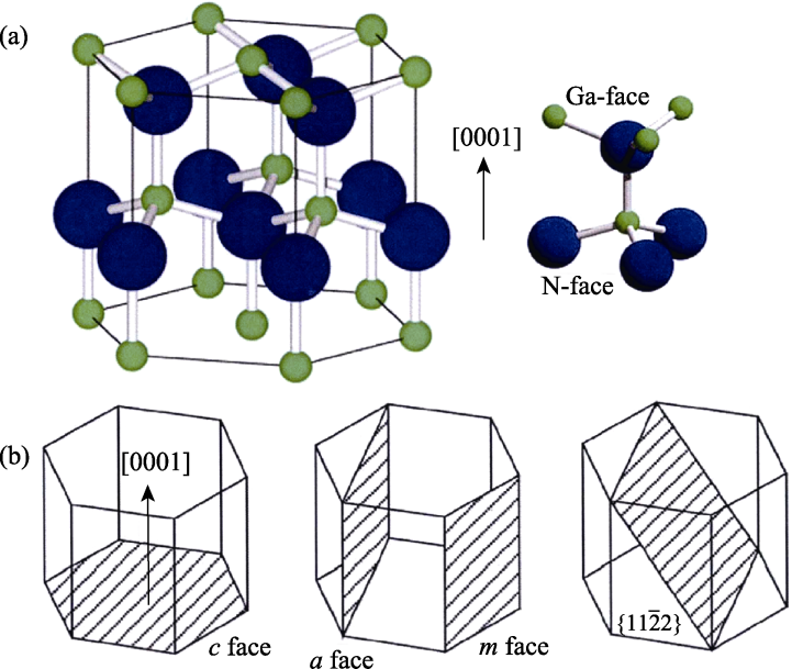
Fig. 1 Schematic diagram of GaN[4] (a) Hexagonal unit call (left) and the bond structure of GaN (right), with green balls indicating Ga atoms and blue balls indicating N atoms; (b) Polar face (left), non-polar face (middle) and one kind of semi-polar faces (right) of GaN crystal
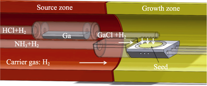
Fig. 2 Structure of HVPE reactor[8]
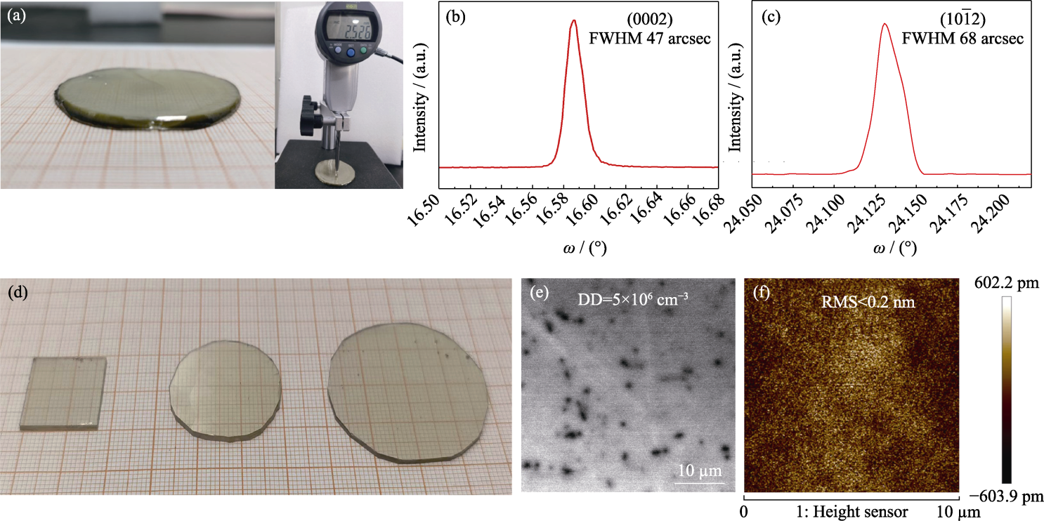
Fig. 3 Photos and characterization of GaN crystals grown by HVPE (a) 2-inch 2.5 mm thick GaN crystal; (b) (0002) surface high-resolution XRD pattern; (c) (10¯12) high-resolution XRD pattern; (d) Image of GaN wafers; (e) CL image (dislocation density ~5×106 cm-2); (f) AFM image (RMS<0.2 nm in the range of 10 μm×10 μm)
| Type | Impurities | Dopant | Characteristic | Application | Ref. |
|---|---|---|---|---|---|
| n type | Si | SiCl2H2 | High carrier concentration; anti-surfactant effect | High power and high current optoelectronic devices (LED, LD) | |
| Ge | GeCl4/Ge3N4 | Little effect on lattice structure and stress, causing no morphological deterioration, higher carriers concentration than that of Si-doped; creating cavities inside the sample | [ | ||
| p type | Mg | Mg(S) | Increased lattice constant and band gap width, high conductivity | Luminescent device | [ |
| Semi- insulating | Fe | Fe(S)/Cp2Fe | High resistivity (iron showing a parasitic effect, easy to diffuse) | High power/frequency devices, HEMT, photoconductive switch, detectors | [ |
| Mn | Mn(S) | ||||
| C | CH4/C2H4/C5H12 |
Table 1 Different types of doped GaN[2-3,32]
| Type | Impurities | Dopant | Characteristic | Application | Ref. |
|---|---|---|---|---|---|
| n type | Si | SiCl2H2 | High carrier concentration; anti-surfactant effect | High power and high current optoelectronic devices (LED, LD) | |
| Ge | GeCl4/Ge3N4 | Little effect on lattice structure and stress, causing no morphological deterioration, higher carriers concentration than that of Si-doped; creating cavities inside the sample | [ | ||
| p type | Mg | Mg(S) | Increased lattice constant and band gap width, high conductivity | Luminescent device | [ |
| Semi- insulating | Fe | Fe(S)/Cp2Fe | High resistivity (iron showing a parasitic effect, easy to diffuse) | High power/frequency devices, HEMT, photoconductive switch, detectors | [ |
| Mn | Mn(S) | ||||
| C | CH4/C2H4/C5H12 |
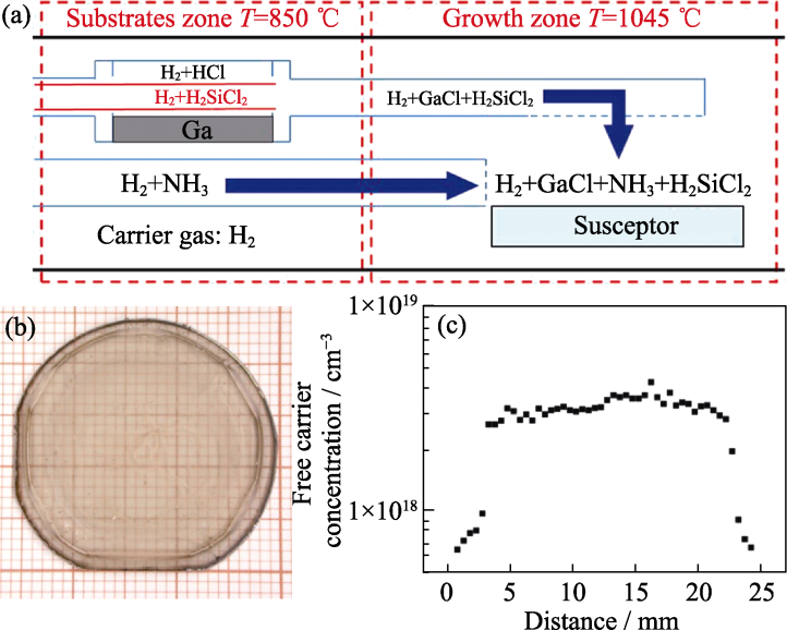
Fig. 4 Si-doped HVPE-GaN[38] (a) Structure of Si-doped HVPE-GaN reactor; (b) Image of 800 μm- thick Si-doped HVPE-GaN; (c) Distribution of free carrier concentration along the diameter of Si-doped HVPE-GaN
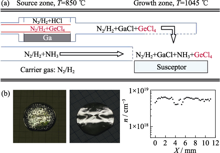
Fig. 5 Ge-doped HVPE-GaN[47] (a) Structure of Ge-doped HVPE-GaN reactor; (b) Morphologies of Ge-doped HVPE-GaN: crystallized in H2 carrier gas (left), crystallized in N2 carrier gas (middle), distribution of free carrier concentration along the diameter of Ge-doped HVPE-GaN
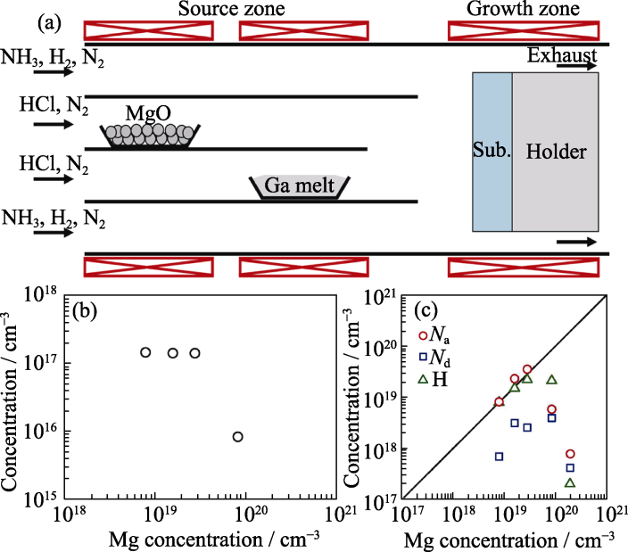
Fig. 6 Mg-doped HVPE-Ga (a) Schematic of the HVPE system for growth of Mg doped GaN using MgO[53]; (b) Hole concentration measured at room temperature as a function of Mg concentration[55]; (c) Compensating donor concentration (Nd) and acceptor concentration (Na) as a function of Mg concentration[55]
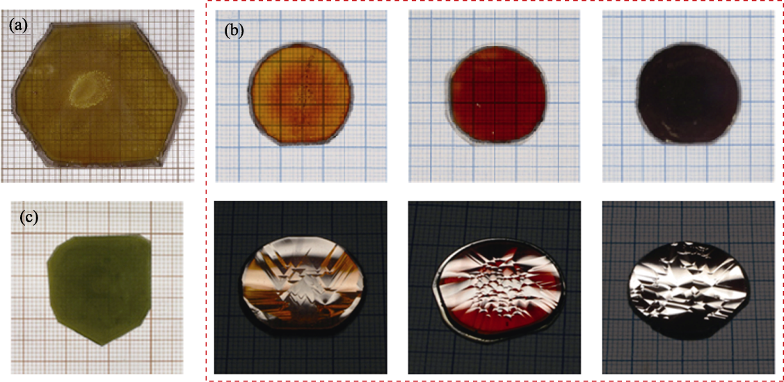
Fig. 7 Image of semi-insulated GaN wafers (a) Fe-doped[62]; (c) Mn-doped[63]; (b) C-doped[60]
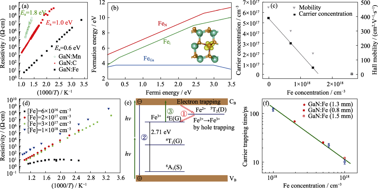
Fig. 8 Fe-doped GaN (a) Resistivity as a function of reciprocal temperature for samples doped with Mn, C, and Fe[8]; (b) Formation energy versus Fermi level for FeGa, FeN and Fei in GaN in different charge states, under Ga-rich conditions[68]; (c) Carrier concentration and Hall mobility versus Fe concentration in GaN films co-doped with Si and Fe[70]; (d) Resistivity versus inverse temperature for samples doped with Fe at various Fe concentrations[63]; (e) Schematic diagram of the energy levels and carrier decay processes of Fe-doped GaN[71]; (f) Carrier trapping time for Fe-doped GaN bulk crystals[72]
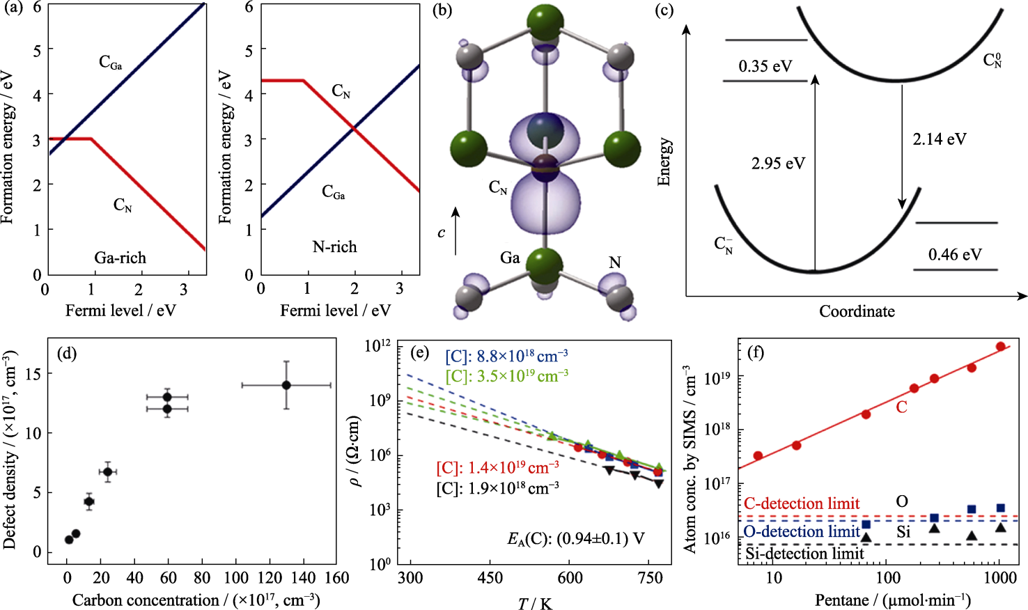
Fig. 9 C-doped GaN (a) Formation energy versus Fermi level for CGa and CN in GaN: Ga-rich conditions (left), and N-rich conditions (right)[79]; (b) CN impurity model in GaN[79]; (c) Optical transitions of CN in GaN[79]; (d) Defect density as a function of C concentration[81]; (e) Temperature-dependent resistivity for C doped GaN[82] ; (f) Concentrations of carbon, oxygen, and silicon in C-doped GaN layers versus the input mole fraction of pentane[82]
| [1] |
HARIMA H. Properties of GaN and related compounds studied by means of Raman scattering. Journal of Physics: Condensed Matter, 2002, 14(38): R967.
DOI URL |
| [2] | ZHANG Y M, WANG J F, CAI D M, et al. Progress on GaN single crystal substrate grown by hydride vapor phase epitaxy. Journal of Synthetic Crystals, 2020, 49(11): 1970. |
| [3] |
ZHANG Y M, WANG J F, CAI D M, et al. Growth and doping of bulk GaN by hydride vapor phase epitaxy. Chinese Physics B, 2020, 29(2): 026104.
DOI |
| [4] | 田媛. HVPE生长自支撑GaN单晶及其性质研究. 济南: 山东大学晶体材料研究所博士学位论文, 2016. |
| [5] | 胡海啸. 自支撑GaN单晶的HVPE生长及加工研究. 济南: 山东大学晶体材料研究所博士学位论文, 2020. |
| [6] |
HSU P S, KELCHNER K M, TYAGI A, et al. InGaN/GaN blue laser diode grown on semipolar (30¯31) free-standing GaN substrates. Applied Physics Express, 2010, 3(5): 052702.
DOI URL |
| [7] |
ABBAS A S, ALYAMANI A Y, NAKAMURA S, et al. Enhancement of n-type GaN (20¯21) semipolar surface morphology in photo-electrochemical undercut etching. Applied Physics Express, 2019, 12(3): 036503.
DOI URL |
| [8] |
BOCKOWSKI M, IWINSKA M, AMILUSIK B, et al. Doping in bulk HVPE-GaN grown on native seeds-highly conductive and semi-insulating crystals. Journal of Crystal Growth, 2018, 499: 1.
DOI URL |
| [9] | VORONENKOV V V, BOCHKAREVA N I, GORBUNOV R I, et al. Two modes of HVPE growth of GaN and related macrodefects. Physica Status Solidi C, 2013, 10(3): 468471. |
| [10] |
LEE M, PARK S. Stress-engineered growth of homoepitaxial GaN crystals using hydride vapor phase epitaxy. RSC Advances, 2018, 8(62): 35571.
DOI URL |
| [11] |
ZHANG L, SHAO Y, HAO X, et al. Improvement of crystal quality HVPE grown GaN on an H3PO4 etched template. CrystEngComm, 2011, 13(15): 5001.
DOI URL |
| [12] | VORONENKOV V V, LELIKOV Y S, ZUBRILOV A S, et al. Thick GaN film stress-induced self-separation. IEEE Conference of Russian Young Researchers in Electrical and Electronic Engineering, St. Petersburg and Moscow, 2019: 833. |
| [13] | MYNBAEVA M, TITKOV A, KRYZHANOVSKI A, et al. Strain relaxation in GaN layers grown on porous GaN sublayers. Materials Research Society Internet Journal of Nitride Semiconductor Research, 1999, 4(14): 1. |
| [14] |
DING S, LI Y W, XIU X Q, et al. Comparison study of GaN films grown on porous and planar GaN templates. Chinese Physics B, 2020, 29(3): 038103.
DOI |
| [15] |
LIU N, JIANG Y, XIAO J, et al. Fabrication of 2-inch free- standing GaN substrate on sapphire with a combined buffer layer by HVPE. Frontiers in Chemistry, 2021, 9: 671720.
DOI URL |
| [16] |
KIM T, JUNG Y H, SONG J, et al. High-efficiency, microscale GaN light-emitting diodes and their thermal properties on unusual substrates. Small, 2012, 8(11): 1643.
DOI URL |
| [17] |
TONG X L, LI L, ZHANG D S, et al. The influences of laser scanning speed on the structural and optical properties of thin GaN films separated from sapphire substrates by excimer laser lift-off. Journal of Physics D: Applied Physics, 2009, 42(4): 045414.
DOI URL |
| [18] |
KIM J, KIM J H, CHO S H, et al. Selective lift-off of GaN light-emitting diode from a sapphire substrate using 266-nm diode-pumped solid-state laser irradiation. Applied Physics A, 2016, 122(4): 1.
DOI URL |
| [19] |
CHU C F, LAI F I, CHU J T, et al. Study of GaN light-emitting diodes fabricated by laser lift-off technique. Journal of Applied Physics, 2004, 95(8): 3916.
DOI URL |
| [20] |
TAVERNIER P R, CLARKE D R. Mechanics of laser-assisted debonding of films. Journal of Applied Physics, 2001, 89(3): 1527.
DOI URL |
| [21] |
UEDA T, ISHIDA M, YURI M. Separation of thin GaN from sapphire by laser lift-off technique. Japanese Journal of Applied Physics, 2011, 50(4R): 041001.
DOI |
| [22] |
FUJIKURA H, KONNO T, SUZUKI T, et al. Macrodefect-free, large, and thick GaN bulk crystals for high-quality 2-6 in. GaN substrates by hydride vapor phase epitaxy with hardness control. Japanese Journal of Applied Physics, 2018, 57(6): 065502.
DOI URL |
| [23] |
FUJIMOTO S, ITAKURA H, TANIKAWA T, et al. Growth of GaN and improvement of lattice curvature using symmetric hexagonal SiO2 patterns in HVPE growth. Japanese Journal of Applied Physics, 2019, 58(SC): SC1049.
DOI URL |
| [24] |
YOSHIDA T, SHIBATA M. GaN substrates having a low dislocation density and a small off-angle variation prepared by hydride vapor phase epitaxy and maskless-3D. Japanese Journal of Applied Physics, 2020, 59(7): 071007.
DOI |
| [25] | MIKAWA Y, ISHINABE T, KAGAMITANI Y, et al. Recent progress of large size and low dislocation bulk GaN growth. Gallium Nitride Materials and Devices XV, 2020, 11280: 1128002. |
| [26] |
SHIM J H, PARK J S, PARK J G. A bow-free freestanding GaN wafer. RSC Advances, 2020, 10(37): 21860.
DOI URL |
| [27] | 中镓半导体: 低位错密度氮化镓自支撑衬底产品量产! 化合物半导体市场(2021-12-29). https://mp.weixin.qq.com/s/eo-ogOy-7hkWgLr0I1vSw. |
| [28] |
LIU L, YU R, WANG G, et al. Fabrication of a 2 inch free standing porous GaN crystal film and application in the growth of relaxed crack-free thick GaN. CrystEngComm, 2021, 23(41): 7245.
DOI URL |
| [29] |
YU R, WANG G, SHAO Y, et al. From bulk to porous GaN crystal: precise structural control and its application in ultraviolet photodetectors. Journal of Materials Chemistry C, 2019, 7(45): 14116.
DOI URL |
| [30] |
ZHANG L, DAI Y, WU Y, et al. Epitaxial growth of a self- separated GaN crystal by using a novel high temperature annealing porous template. CrystEngComm, 2014, 16(38): 9063.
DOI URL |
| [31] |
LIU L, ZHANG X, WANG S, et al. Nucleation mechanism of GaN crystal growth on porous GaN/sapphire substrates. CrystEngComm, 2022, 24(10): 1840.
DOI URL |
| [32] | CAI L L, FENG C J. First-principles study on the electronic structure and optical properties of GaN with Mg doped. Journal of North China Institute of Science and Technology, 2019, 16(4): 120. |
| [33] |
XIE Z, SUI Y, BUCKERIDGE J, et al. Demonstration of the donor characteristics of Si and O defects in GaN using hybrid QM/MM. Physica Status Solidi (A), 2017, 214(4): 1600445.
DOI URL |
| [34] |
FREITAS J A. Pervasive shallow donor impurities in GaN. ECS Journal of Solid State Science and Technology, 2019, 9(1): 015009.
DOI URL |
| [35] | VAUDO R P, XU X, SALANT A D, et al. Background impurity reduction and iron doping of gallium nitride wafers. MRS Online Proceedings Library (OPL), 2002, 743: 207. |
| [36] | LIPSKI F. Si-doped GaN by Hydride-vapour-phase-epitaxy Using a Ga: Si-solution as Doping Source. Annual Report, Institute of Optoelectronics, Ulm University, 2007: 53. |
| [37] |
RICHTER E, HENNIG C, ZEIMER U, et al. N-type doping of HVPE-grown GaN using dichlorosilane. Physica Status Solidi (A), 2006, 203(7): 1658.
DOI URL |
| [38] |
IWINSKA M, SOCHACKI T, AMILUSIK M, et al. Homoepitaxial growth of HVPE-GaN doped with Si. Journal of Crystal Growth, 2016, 456: 91.
DOI URL |
| [39] |
MARKURT T, LYMPERAKIS L, NEUGEBAUER J, et al. Blocking growth by an electrically active subsurface layer: the effect of Si as an antisurfactant in the growth of GaN. Physical Review Letters, 2013, 110(3): 036103.
DOI URL |
| [40] |
XIE J, MITA S, HUSSEY L, et al. On the strain in n-type GaN. Applied Physics Letters, 2011, 99(14): 141916.
DOI URL |
| [41] |
FRITZE S, DADGAR A, WITTE H, et al. High Si and Ge n-type doping of GaN doping-limits and impact on stress. Applied Physics Letters, 2012, 100(12): 122104.
DOI URL |
| [42] |
RICHTER E, STOICA T, ZEIMER U, et al. Si doping of GaN in hydride vapor-phase epitaxy. Journal of Electronic Materials, 2013, 42(5): 820.
DOI URL |
| [43] |
XIA S Y, ZHANG Y M, WANG J F, et al. HVPE growth of bulk GaN with high conductivity for vertical devices. Semiconductor Science and Technology, 2021, 36(1): 014009.
DOI |
| [44] |
OSHIMA Y, YOSHIDA T, WATANABE K, et al. Properties of Ge-doped, high-quality bulk GaN crystals fabricated by hydride vapor phase epitaxy. Journal of Crystal Growth, 2010, 312(24): 3569.
DOI URL |
| [45] |
WIENEKE M, WITTE H, LANGE K, et al. Ge as a surfactant in metal-organic vapor phase epitaxy growth of a-plane GaN exceeding carrier concentrations of 1020 cm-3. Applied Physics Letters, 2013, 103(1): 012103.
DOI URL |
| [46] |
BOGUSŁAWSKI P, BERNHOLC J. Doping properties of C, Si, and Ge impurities in GaN and AlN. Physical Review B, 1997, 56(15): 9496.
DOI URL |
| [47] |
IWINSKA M, TAKEKAWA N, IVANOV V Y, et al. Crystal growth of HVPE-GaN doped with germanium. Journal of Crystal Growth, 2017, 480: 102.
DOI URL |
| [48] |
ZHANG Y M, WANG J F, SU X J, et al. Investigation of pits in Ge-doped GaN grown by HVPE. Japanese Journal of Applied Physics, 2019, 58(12): 120910.
DOI URL |
| [49] | USIKOV A, KOVALENKOV O, SOUKHOVEEV V, et al. Electrical and optical properties of thick highly doped p-type GaN layers grown by HVPE. Physica Status Solidi (c), 2008, 5(6): 1829. |
| [50] |
NAKAMURA S, IWASA N, SENOH M S M, et al. Hole compensation mechanism of p-type GaN films. Japanese Journal of Applied Physics, 1992, 31(5R): 1258.
DOI |
| [51] |
AMANO H, KITO M, HIRAMATSU K, et al. P-type conduction in Mg-doped GaN treated with low-energy electron beam irradiation (LEEBI). Japanese Journal of Applied Physics, 1989, 28(12A): L2112.
DOI |
| [52] | TONG Y Z, LI F, YANG Z J, et al. Electrical property and annealing characteristics of heavy Mg-doped GaN films. Semiconductor Optoelectronics, 2001, 22(2): 140. |
| [53] |
OHNISHI K, AMANO Y, FUJIMOTO N, et al. Halide vapor phase epitaxy of p-type Mg-doped GaN utilizing MgO. Applied Physics Express, 2020, 13(6): 061007.
DOI URL |
| [54] |
KIMURA T, OHNISHI K, AMANO Y, et al. Thermodynamic analysis of the gas phase reaction of Mg-doped GaN growth by HVPE using MgO. Japanese Journal of Applied Physics, 2020, 59(8): 088001.
DOI URL |
| [55] | OHNISHI K, AMANO Y, FUJIMOTO N, et al. Electrical properties and structural defects of p-type GaN layers grown by halide vapor phase epitaxy. Journal of Crystal Growth, 2021, 566: 126173. |
| [56] |
ROMANO L T, KNEISSL M, NORTHRUP J E, et al. Influence of microstructure on the carrier concentration of Mg-doped GaN films. Applied Physics Letters, 2001, 79(17): 2734.
DOI URL |
| [57] |
TETSUO N, NOBUYUKI I, KAZUYOSHI T, et al. Wide range doping control and defect characterization of GaN layers with various Mg concentrations. Journal of Applied Physics, 2018, 124(16): 165706.
DOI URL |
| [58] |
HORITA M, TAKASHIMA S, TANAKA R, et al. Hall-effect measurements of metalorganic vapor-phase epitaxy-grown p-type homoepitaxial GaN layers with various Mg concentrations. Japanese Journal of Applied Physics, 2017, 56(3): 031001.
DOI URL |
| [59] |
HEITZ R, MAXIM P, ECKEY L, et al. Excited states of Fe3+ in GaN. Physical Review B, 1997, 55: 4382.
DOI URL |
| [60] |
IWINSKA M, PIOTRZKOWSKI R, LITWIN-STASZEWSKA E, et al. Highly resistive C-doped hydride vapor phase epitaxy-GaN grown on ammonothermally crystallized GaN seeds. Applied Physics Express, 2016, 10(1): 011003.
DOI |
| [61] |
FREITAS JR J A, TISCHLER J G, KIM J H, et al. Properties of Fe-doped semi-insulating GaN substrates for high-frequency device fabrication. Journal of Crystal Growth, 2007, 305(2): 403.
DOI URL |
| [62] |
IWINSKA M, PIOTRZKOWSKI R, LITWIN-STASZEWSKA E, et al. Crystallization of semi-insulating HVPE-GaN with solid iron as a source of dopants. Journal of Crystal Growth, 2017, 475: 121.
DOI URL |
| [63] |
IWINSKA M, ZAJAC M, LUCZNIK B, et al. Iron and manganese as dopants used in the crystallization of highly resistive HVPE-GaN on native seeds. Japanese Journal of Applied Physics, 2019, 58(SC): SC1047.
DOI URL |
| [64] |
VAUDO R P, XU X, SALANT A, et al. Characteristics of semi-insulating, Fe-doped GaN substrates. Physica Status Solidi (A), 2003, 200(1): 18.
DOI URL |
| [65] |
BAUR J, MAIER K, KUNZER M, et al. Infrared luminescence of residual iron deep level acceptors in gallium nitride (GaN) epitaxial layers. Applied Physics Letters, 1994, 64(7): 857.
DOI URL |
| [66] |
CORDIER Y, AZIZE M, BARON N, et al. Subsurface Fe-doped semi-insulating GaN templates for inhibition of regrowth interface pollution in AlGaN/GaN HEMT structures. Journal of Crystal Growth, 2008, 310(5): 948.
DOI URL |
| [67] |
ZHENG C C, NING J Q, WU Z P, et al. Effects of Fe doping on the strain and optical properties of GaN epilayers grown on sapphire substrates. RSC Advances, 2014, 4(98): 55430.
DOI URL |
| [68] |
WICKRAMARATNE D, SHEN J X, DREYER C E, et al. Iron as a source of efficient Shockley-Read-Hall recombination in GaN. Applied Physics Letters, 2016, 109(16): 162107.
DOI URL |
| [69] | 周淼. Fe掺杂GaN材料电子结构与光学特性的研究. 西安: 西安理工大学硕士学位论文, 2018. |
| [70] |
HEIKMAN S, KELLER S, MATES T, et al. Growth and characteristics of Fe-doped GaN. Journal of Crystal Growth, 2003, 248: 513.
DOI URL |
| [71] |
FANG Y, YANG J, LI Z, et al. Optical nonlinearities and carrier dynamics in Fe doped GaN single crystal. Applied Physics Letters, 2014, 105(16): 161909.
DOI URL |
| [72] |
FANG Y, WU X, YANG J, et al. Effect of Fe-doping on nonlinear optical responses and carrier trapping dynamics in GaN single crystals. Applied Physics Letters, 2015, 107(5): 051901.
DOI URL |
| [73] |
ČĖSNA A, SÖDERSTRÖM D, MARCINKEVIČIUS S, et al. Carrier trapping in iron-doped GaInP. Journal of Applied Physics, 1999, 85(2): 1234.
DOI URL |
| [74] |
RICHTER E, GRIDNEVA E, WEYERS M, et al. Fe-doping in hydride vapor-phase epitaxy for semi-insulating gallium nitride. Journal of Crystal Growth, 2016, 456: 97.
DOI URL |
| [75] |
FREITAS J A, CULBERTSON J C, GLASER E R, et al. Efficient iron doping of HVPE GaN. Journal of Crystal Growth, 2018, 500: 111.
DOI URL |
| [76] |
ZVANUT M E, PAUDEL S, GLASER E R, et al. Incorporation of carbon in free-standing HVPE-grown GaN substrates. Journal of Electronic Materials, 2019, 48(4): 2226.
DOI |
| [77] | ZHOU D, NI Y, HE Z, et al. Investigation of breakdown properties in the carbon doped GaN by photoluminescence analysis. Physica Status Solidi (C), 2016, 13(5/6): 345. |
| [78] |
PIOTRZKOWSKI R, ZAJAC M, LITWIN-STASZEWSKA E, et al. Self-compensation of carbon in HVPE-GaN:C. Applied Physics Letters, 2020, 117(1): 012106.
DOI URL |
| [79] |
LYONS J L, JANOTTI A, VAN DE WALLE C G. Carbon impurities and the yellow luminescence in GaN. Applied Physics Letters, 2010, 97(15): 152108.
DOI URL |
| [80] | RESHCHIKOV M A, VOROBIOV M, DEMCHENKO D O, et al. Two charge states of the CN acceptor in GaN: evidence from photoluminescence. Physical Review B, 2018, 98(12): 125207. |
| [81] |
ZVANUT M E, PAUDEL S, SUNAY U R, et al. Charge transfer process for carbon-related center in semi-insulating carbon-doped GaN. Journal of Applied Physics, 2018, 124(7): 075701.
DOI URL |
| [82] |
RICHTER E, BEYER F C, ZIMMERMANN F, et al. Growth and properties of intentionally carbon-doped GaN layers. Crystal Research and Technology, 2020, 55(2): 1900129.
DOI URL |
| [83] |
KLEIN P B, BINARI S C, IKOSSI K, et al. Current collapse and the role of carbon in AlGaN/GaN high electron mobility transistors grown by metalorganic vapor-phase epitaxy. Applied Physics Letters, 2001, 79(21): 3527.
DOI URL |
| [84] |
FUJIKURA H, HAYASHI K, HORIKIRI F, et al. Elimination of macrostep-induced current flow nonuniformity in vertical GaN PN diode using carbon-free drift layer grown by hydride vapor phase epitaxy. Applied Physics Express, 2018, 11(4): 045502.
DOI URL |
| [85] | LAI Y, LUO X J, WANG X Y. C-doped semi-insulating GaN grown by HVPE. Guangdong Chemical Industry, 2021, 48(9): 13. |
| [86] |
LYONS J L, GLASER E R, ZVANUT M E, et al. Carbon complexes in highly C-doped GaN. Physical Review B, 2021, 104(7): 075201.
DOI URL |
| [1] | CHEN Mingjun, MIAO Hongkang, XIAO Yingjun, DENG Jianbo, ZHANG Xiang, ZHAO Jiupeng, LI Yao. Photo- and Thermo-chromic Dual-responsive Materials: A Review on Design Strategies and Applications in Smart Windows [J]. Journal of Inorganic Materials, 2026, 41(6): 723-738. |
| [2] | SONG Kunjie, XIE Rongjun. Research Advances on Machine Learning-driven Development of Novel Luminescent Materials [J]. Journal of Inorganic Materials, 2026, 41(6): 689-703. |
| [3] | HU Yuqing, ZHU Yixin, LE Xianhao, WAN Qing. Lithium Tantalate Wafer: Advances in Thinning Technology and Application in Pyroelectric Infrared Detectors [J]. Journal of Inorganic Materials, 2026, 41(6): 764-774. |
| [4] | LIU Chunfan, CHEN Ke, GE Fangfang, HUANG Qing. Research Progress on Lead-bismuth Eutectic Corrosion Resistant Coatings [J]. Journal of Inorganic Materials, 2026, 41(6): 775-786. |
| [5] | HU Yang, XIE Min, ZHANG Xiaoyi, LI Xiang, GUO Xinwei, JIANG Nan, ZHOU Wenhan, ZHANG Shengli, ZENG Haibo. Research Progress on Computational and Data-driven Environmental-friendly Luminescent Materials [J]. Journal of Inorganic Materials, 2026, 41(6): 704-722. |
| [6] | WANG Junbu, HUANG Zeai, YANG Mingkai, MENG Ying, ZHOU Mingwei, ZHOU Ying. Research Progress on Anti-coking Catalytic Materials for Methane Conversion [J]. Journal of Inorganic Materials, 2026, 41(6): 739-750. |
| [7] | WANG Jinwen, YANG Zhen, ZHOU Huan, XIA Dan, YANG Lei. Biomedical Applications of Injectable Inorganic Biomaterials [J]. Journal of Inorganic Materials, 2026, 41(6): 751-763. |
| [8] | LI Hantao, SHEN Qiang, LUO Guoqiang, WANG Xuefei, GAO Ming, CHEN Chen. Research Progress on Structure and Performance Regulation of Silicon-based Anode Materials via Mechanical Ball Milling [J]. Journal of Inorganic Materials, 2026, 41(5): 561-572. |
| [9] | XIE Chenyi, MIAO Huaming, ZHANG Weiran, LIU Rongjun, WANG Yanfei, LI Duan. Research Progress on Theoretical Calculation in the Field of High-entropy Ceramics [J]. Journal of Inorganic Materials, 2026, 41(5): 545-560. |
| [10] | QIAN Xinyu, WANG Wudi, GUO Junyao, REN Yongchun, DONG Jianshu, WANG Qingguo, TANG Huili, ZHANG Chenbo, XU Xiaodong, DONG Yongjun, HUA Wei, XU Jun. Spectroscopic Analysis of Ho:BaF2 Crystals in the NIR to MIR Spectral Region [J]. Journal of Inorganic Materials, 2026, 41(5): 595-603. |
| [11] | LI Xuan, YE Kuicai, FENG Jiayin, QIU Jiajun, QIAN Wenhao, XING Min. Surface Modification of Titanium-based Dental Implants for Soft Tissue Sealing: A Review [J]. Journal of Inorganic Materials, 2026, 41(4): 432-444. |
| [12] | MA Xiaojia, GENG Xinyu, ZHANG Weike. Boron and Nitrogen Co-doped Biomass Carbon Sphere Anode Material: Preparation and Sodium Storage Properties for Sodium-ion Batteries [J]. Journal of Inorganic Materials, 2026, 41(4): 469-478. |
| [13] | XU Hao, GU Haitao, WU Honghui, YUE Xiaofei, LIN Siqi, JIN Min. Crystal Growth and Properties of Bi-doped InSe [J]. Journal of Inorganic Materials, 2026, 41(4): 493-499. |
| [14] | PENG Dezhao, LI Rui, WANG Wenhong, WANG Zirui, ZHANG Zhizhen. Research Progress on Sodium Chloride Solid Electrolytes [J]. Journal of Inorganic Materials, 2026, 41(4): 409-420. |
| [15] | CHEN Kun, JIANG Yonggang, FENG Junzong, LI Liangjun, HU Yijie, FENG Jian. Research Progress on Lanthanum Zirconate Porous Materials for Thermal Insulation [J]. Journal of Inorganic Materials, 2026, 41(4): 421-431. |
| Viewed | ||||||
|
Full text |
|
|||||
|
Abstract |
|
|||||