无机材料学报 ›› 2024, Vol. 39 ›› Issue (4): 416-422.DOI: 10.15541/jim20230392 CSTR: 32189.14.10.15541/jim20230392
所属专题: 【AI4材料】Al4材料(202512); 【信息功能】功能晶体(202512)
王伟华1( ), 张磊宁2, 丁峰3(), 代兵4(), 韩杰才4, 朱嘉琦4, 贾怡1, 杨宇5
收稿日期:2023-08-30
修回日期:2023-11-06
出版日期:2024-04-20
网络出版日期:2023-11-28
通讯作者:
丁 峰, 教授. E-mail: f.ding@siat.ac.cn;作者简介:王伟华(1992-), 男, 博士. E-mail: weihuawang2011@163.com
基金资助:
WANG Weihua1(), ZHANG Leining2, DING Feng3(), DAI Bing4(), HAN Jiecai4, ZHU Jiaqi4, JIA Yi1, Yang Yu5
Received:2023-08-30
Revised:2023-11-06
Published:2024-04-20
Online:2023-11-28
Contact:
DING Feng, professor. E-mail: f.ding@siat.ac.cn;About author:WANG Weihua (1992-), male, PhD. E-mail: weihuawang2011@163.com
Supported by:摘要:
异质外延为金刚石晶圆合成提供了一个有效的实现路径, 而Ir衬底上金刚石形核生长技术经过20多年的发展已经有能力制备最大直径为3.5英寸的晶体, 开启了金刚石作为终极半导体在电子信息产业应用的大门。然而,表面形核、偏压技术窗口、金刚石外延生长等一系列发生在异质衬底上的问题都需要从生长热力学的角度给予解释。本研究针对化学气相沉积气氛中金刚石如何实现外延形核与生长这一关键问题, 利用第一性原理计算从原子尺度对金刚石形核生长过程展开了系列探究。研究结果如下: C原子在Ir衬底表面位点吸附比在体相位点吸附更稳定, 表明无偏压条件下金刚石形核只能在衬底表面发生; 离子轰击作用下非晶氢化碳层中sp3杂化C原子个数随着离子动能的增加呈现先增大后减小的变化规律, 证实了金刚石高密度形核存在一定的离子动能与偏压大小窗口; 金刚石沿着Ir衬底外延生长时界面结合能最低(约为-0.58 eV/C), 意味着界面结合能是决定外延形核生长的主要热力学因素。本研究阐明了偏压辅助离子轰击促进金刚石单晶外延生长的热力学机制, 对于指导金刚石及其他碳基半导体生长具有重要意义。
中图分类号:
王伟华, 张磊宁, 丁峰, 代兵, 韩杰才, 朱嘉琦, 贾怡, 杨宇. 铱衬底上金刚石外延形核与生长: 第一性原理计算[J]. 无机材料学报, 2024, 39(4): 416-422.
WANG Weihua, ZHANG Leining, DING Feng, DAI Bing, HAN Jiecai, ZHU Jiaqi, JIA Yi, Yang Yu. Heteroepitaxial Diamond Nucleation and Growth on Iridium: First-principle Calculation[J]. Journal of Inorganic Materials, 2024, 39(4): 416-422.
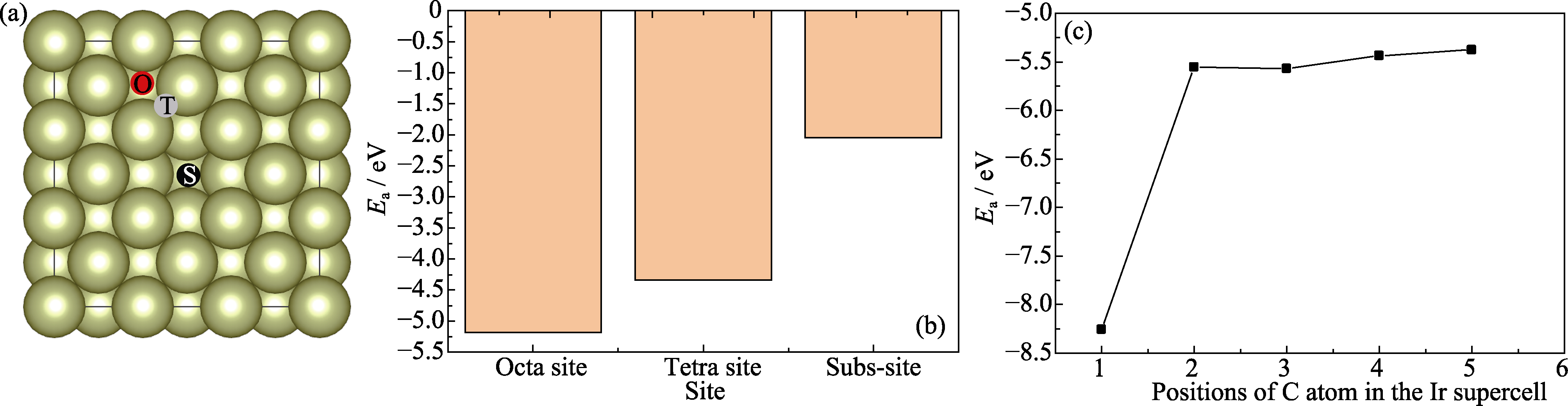
图1 C原子在Ir衬底上的吸附模型及行为
Fig. 1 Adsorption modes and behaviors of C atom on Ir substrate (a) Adsorption modes of C atom in octa-site (O), tetra-site (T) and subs-site (S) of the surface; (b) Adsorption energy when one C atom is adsorbed on different sites of Ir substrate; (c) Adsorption energy variation of C atoms adsorbed on different depths from Ir (001) surface
| Ion rate | 0.005 nm/fs | 0.011 nm/fs | 0.019 nm/fs | 0.025 nm/fs | 0.030 nm/fs | 0.035 nm/fs | ||||||
|---|---|---|---|---|---|---|---|---|---|---|---|---|
| Number Step | C atom | sp3-C atom | C atom | sp3-C atom | C atom | sp3-C atom | C atom | sp3-C atom | C atom | sp3-C atom | C atom | sp3-C atom |
| 2500 | 4 | 0 | 4 | 0 | 6 | 0 | 6 | 0 | 6 | 0 | 6 | 0 |
| 5000 | 9 | 0 | 7 | 1 | 9 | 0 | 11 | 0 | 11 | 0 | 11 | 0 |
| 7500 | 6 | 0 | 13 | 1 | 15 | 0 | 15 | 0 | 17 | 0 | 17 | 1 |
| 10000 | - | 16 | 3 | 21 | 1 | 17 | 2 | 20 | 2 | 23 | 1 | |
| 12500 | 21 | 4 | 22 | 1 | 18 | 2 | 23 | 0 | 26 | 1 | ||
| 15000 | 17 | 5 | - | - | - | - | - | |||||
表1 不同速率CH3+离子轰击表面后形成a-C:H层中C原子个数及sp3-C原子个数.
Table 1 Carbon atom number and sp3-bonded carbon number in the a-C:H layer after the CH3+ ion bombardment with different rates
| Ion rate | 0.005 nm/fs | 0.011 nm/fs | 0.019 nm/fs | 0.025 nm/fs | 0.030 nm/fs | 0.035 nm/fs | ||||||
|---|---|---|---|---|---|---|---|---|---|---|---|---|
| Number Step | C atom | sp3-C atom | C atom | sp3-C atom | C atom | sp3-C atom | C atom | sp3-C atom | C atom | sp3-C atom | C atom | sp3-C atom |
| 2500 | 4 | 0 | 4 | 0 | 6 | 0 | 6 | 0 | 6 | 0 | 6 | 0 |
| 5000 | 9 | 0 | 7 | 1 | 9 | 0 | 11 | 0 | 11 | 0 | 11 | 0 |
| 7500 | 6 | 0 | 13 | 1 | 15 | 0 | 15 | 0 | 17 | 0 | 17 | 1 |
| 10000 | - | 16 | 3 | 21 | 1 | 17 | 2 | 20 | 2 | 23 | 1 | |
| 12500 | 21 | 4 | 22 | 1 | 18 | 2 | 23 | 0 | 26 | 1 | ||
| 15000 | 17 | 5 | - | - | - | - | - | |||||
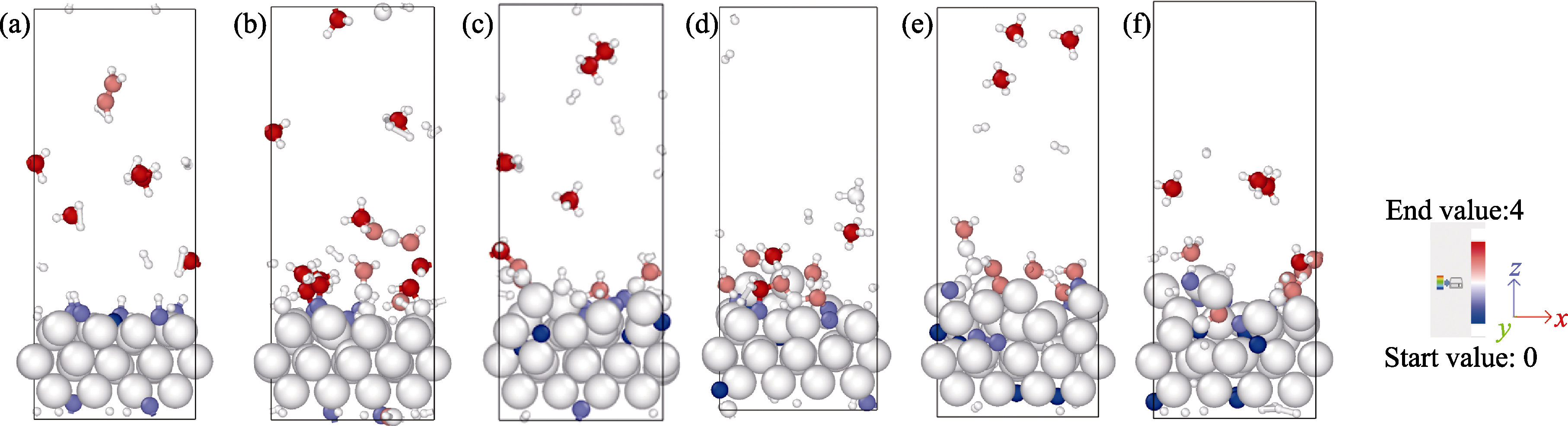
图2 不同速率CH3+离子轰击表面后所有C原子的成键类型
Fig. 2 Bonding types of C atoms after the CH3+ ion bombardment with different ion rates (a) 0.005 nm/fs; (b) 0.011 nm/fs; (c) 0.019 nm/fs; (d) 0.025 nm/fs; (e) 0.030 nm/fs; (f) 0.035 nm/fs Atoms with the atomic size from large to small representing Ir, C and H, and C atom with the color from blue to red representing the bonding number of C atom from 0 to 4. Colorful figures are available on website
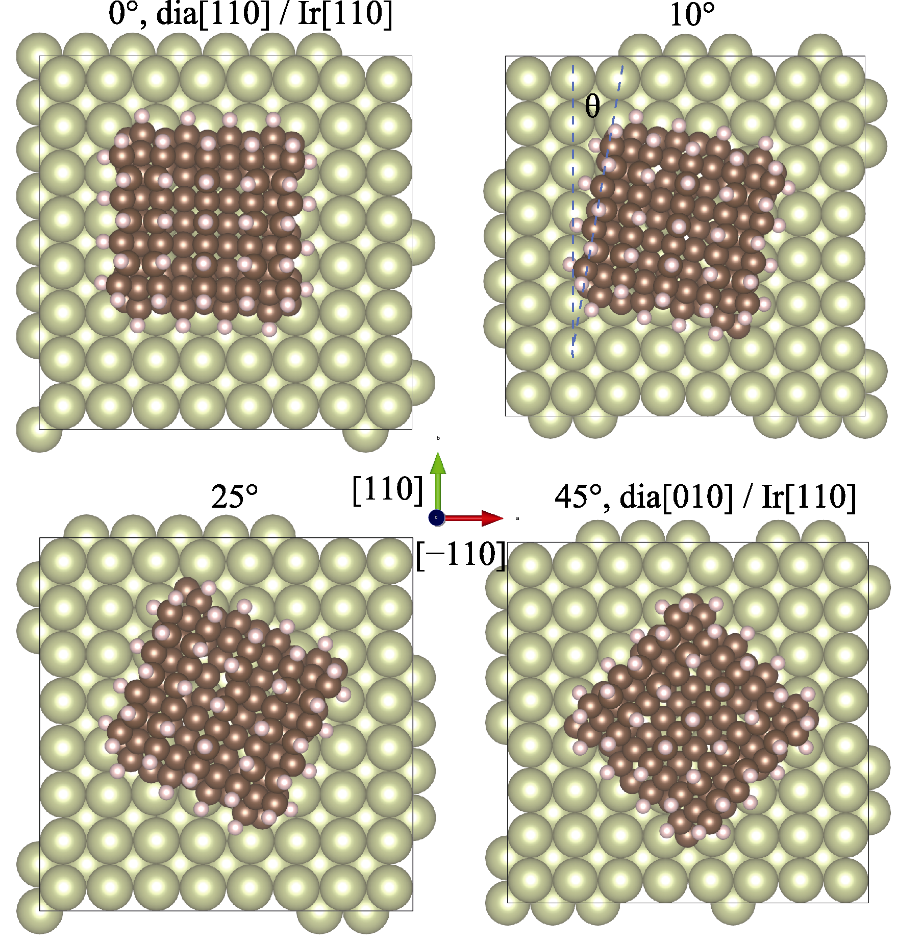
图3 金刚石(001)团簇与Ir(001)衬底夹角θ=0°、10°、25°和45°时的结构
Fig. 3 Structure of cluster model of diamond (001) and Ir (001) surface as a function of the alignment angle θ=0°, 10°, 25° and 45° When θ are 0° and 45°, the in-plane orientation relationships are diamond(001)[010]//Ir(001)[010] and diamond(001)[110]//Ir(001)[010], respectively

图4 金刚石-Ir体系结合能随夹角θ的变化关系(a), 及金刚石在Ir(001)衬底上进行形核生长后获得的SEM表面形貌(b)
Fig. 4 Binding energy for the diamond-Ir system as a function of the alignment angle θ (a), and SEM surface morphology of diamond grains on Ir (001) surface (b) No.1-4 represent grains with different sizes and shapes
| [1] | PARK K, LEE H-P, VAN DUREN J K J, et al. Single crystal diamond: an ultimate semiconductor. Chicago: Office of Science, U.S. Department of Energy, 2020. |
| [2] |
DANG C, CHOU J P, DAI B, et al. Achieving large uniform tensile elasticity in microfabricated diamond. Science, 2021, 371(6524): 76.
DOI PMID |
| [3] |
ALHASANI R, YABE T, IYAMA Y, et al. An enhanced two-dimensional hole gas (2DHG) C-H diamond with positive surface charge model for advanced normally-off MOSFET devices. Scientific Reports, 2022, 12: 4203.
DOI PMID |
| [4] |
LIU B, BI T, FU Y, et al. MOSFETs on (110) C-H diamond: ALD Al2O3/diamond interface analysis and high performance normally- OFF operation realization. IEEE Transactions on Electron Devices, 2022, 69(3): 949.
DOI URL |
| [5] |
BERDERMANN E, AFANACIEV K, CIOBANU M, et al. Progress in detector properties of heteroepitaxial diamond grown by chemical vapor deposition on Ir/YSZ/Si (001) wafers. Diamond and Related Materials, 2019, 97: 107420.
DOI URL |
| [6] |
LIAO M. Progress in semiconductor diamond photodetectors and MEMS sensors. Functional Diamond, 2021, 1(1): 29.
DOI URL |
| [7] |
SHIMAOKA T, KOIZUMI S J H, et al. Recent progress in diamond radiation detectors. Functional Diamond, 2021, 1(1): 205.
DOI URL |
| [8] |
ARNAULT J C, LEE K H, DELCHEVALRIE J, et al. Epitaxial diamond on Ir/SrTiO3/Si (001): from sequential material characterizations to fabrication of lateral schottky diodes. Diamond and Related Materials, 2020, 105: 107768.
DOI URL |
| [9] |
ACHARD J, JACQUES V, TALLAIRE A. Chemical vapour deposition diamond single crystals with nitrogen-vacancy centres: a review of material synthesis and technology for quantum sensing applications. Journal of Physics D: Applied Physics, 2020, 53(31): 313001.
DOI URL |
| [10] |
HO K O, SHEN Y, PANG Y Y, et al. Diamond quantum sensors: from physics to applications on condensed matter research. Functional Diamond, 2021, 1(1): 160.
DOI URL |
| [11] |
SANG L. Diamond as the heat spreader for the thermal dissipation of GaN-based electronic devices. Functional Diamond, 2021, 1(1): 174.
DOI URL |
| [12] |
YANG Q, ZHAO J, HUANG Y, et al. A diamond made microchannel heat sink for high-density heat flux dissipation. Applied Thermal Engineering, 2019, 158: 113804.
DOI URL |
| [13] |
LU W, LI J, MIAO J, et al. Application of high-thermal- conductivity diamond for space phased array antenna. Functional Diamond, 2021, 1(1): 189.
DOI URL |
| [14] |
GEIS M W, SMITH H I, ARGOITIA A, et al. Large‐area mosaic diamond films approaching single-crystal quality. Applied Physics Letters, 1991, 58(22): 2485.
DOI URL |
| [15] |
YAMADA H, CHAYAHARA A, MOKUNO Y, et al. A 2-in. mosaic wafer made of a single-crystal diamond. Applied Physics Letters, 2014, 104(10): 102110.
DOI URL |
| [16] |
YELISSEYEV A P, ZHIMULEV E I, KARPOVICH Z A, et al. Characterization of the nitrogen state in HPHT diamonds grown in an Fe-C melt with a low sulfur addition. CrystEngComm, 2022, 24: 4408.
DOI URL |
| [17] |
CHERNYKH S V, CHERNYKH A V, TARELKIN S A, et al. High-pressure high-temperature single-crystal diamond type IIa characterization for particle detectors. Physica Status Solidi (a), 2020, 217(8): 1900888.
DOI URL |
| [18] |
CHARRIS A, NAD S, ASMUSSEN J. Exploring constant substrate temperature and constant high pressure SCD growth using variable pocket holder depths. Diamond and Related Materials, 2017, 76: 58.
DOI URL |
| [19] |
WANG W, LIU B, ZHANG L, et al. Heteroepitaxy of diamond semiconductor on iridium: a review. Functional Diamond, 2022, 2(1): 215.
DOI URL |
| [20] |
SCHRECK M, HÖRMANN F, ROLL H, et al. Diamond nucleation on iridium buffer layers and subsequent textured growth: a route for the realization of single-crystal diamond films. Applied Physics Letters, 2001, 78(2): 192.
DOI URL |
| [21] |
SCHRECK M, GSELL S, BRESCIA R, et al. Ion bombardment induced buried lateral growth: the key mechanism for the synthesis of single crystal diamond wafers. Scientific Reports, 2017, 7: 44462.
DOI PMID |
| [22] |
ARGOITIA A, ANGUS J C, MA J S, et al. Heteroepitaxy of diamond on C-BN: growth mechanisms and defect characterization. Journal of Materials Research, 1994, 9(7): 1849.
DOI URL |
| [23] |
SHINTANI Y. Growth of highly (111)-oriented, highly coalesced diamond films on platinum (111) surface: a possibility of heteroepitaxy. Journal of Materials Research, 1996, 11(12): 2955.
DOI URL |
| [24] |
HOFFMAN A, MICHAELSON S H, AKHVLEDIANI R, et al. Comparison of diamond bias enhanced nucleation on Ir and 3C-SiC: a high resolution electron energy loss spectroscopy study. Physica Status Solidi (a), 2009, 206(9): 1972.
DOI URL |
| [25] |
SCHRECK M, THÜRER K-H, STRITZKER B. Limitations of the process window for the bias enhanced nucleation of heteroepitaxial diamond films on silicon in the time domain. Journal of Applied Physics, 1997, 81(7): 3092.
DOI URL |
| [26] | SCHRECK M. Single Crystal Diamond Growth on Iridium// Comprehensive Hard Materials. Elsevier, 2014: 269-304. |
| [27] | WANG Y, ZHU J, HU Z, et al. Heteroepitaxial growth of single crystal diamond films on iridium: procedure and mechanism. Journal of Inorganic Materials, 2019, 39(9): 909. |
| [28] |
WANG W, WANG Y, SHU G, et al. Recent progress in hetero-epitaxial growth of the single-crystal diamond. Scientia Sinica Technologica, 2020, 50(7): 831.
DOI URL |
| [29] |
CHIANG M J, HON M H. Optical emission spectroscopy study of positive direct current bias enhanced diamond nucleation. Thin Solid Films, 2008, 516(15): 4765.
DOI URL |
| [30] |
CHAVANNE A, ARNAULT J-C, BARJON J, et al. Bias-enhanced nucleation of diamond on iridium: a comprehensive study of the first stages by sequential surface analysis. Surface Science, 2011, 605(5/6): 564.
DOI URL |
| [31] | CHAVANNE A, ARNAULT J C, BARJON J, et al. Effect of bias voltage on diamond nucleation on iridium during BEN. AIP Conference Proceedings, 2010, 1292(1): 137. |
| [32] |
OHTSUKA K, SUZUKI K, SAWABE A, et al. Epitaxial growth of diamond on iridium. Japanese Journal of Applied Physics, 1996, 35: L1072.
DOI |
| [33] |
CHEN G, WANG W, LIN F, et al. Electrical characteristics of diamond MOSFET with 2DHG on a heteroepitaxial diamond substrate. Materials, 2022, 15(7): 2557.
DOI URL |
| [34] | YOSHIKAWA T, HERRLING D, MEYER F, et al. Influence of substrate holder configurations on bias enhanced nucleation area for diamond heteroepitaxy: toward wafer-scale single-crystalline diamond synthesis. Journal of Vacuum Science & Technology B, 2019, 37(2): 021207. |
| [35] |
KIM S-W, KAWAMATA Y, TAKAYA R, et al. Growth of high-quality one-inch free-standing heteroepitaxial (001) diamond on ($11\bar{2}0$) sapphire substrate. Applied Physics Letters, 2020, 117(20): 202102.
DOI URL |
| [36] |
KIM S-W, TAKAYA R, HIRANO S, et al. Two-inch high-quality (001) diamond heteroepitaxial growth on sapphire ($11\bar{2}0$) misoriented substrate by step-flow mode. Applied Physics Express, 2021, 14(11): 115501.
DOI |
| [37] |
WANG W, YANG S, HAN J, et al. Role of surface chemistry in determining the heteroepitaxial growth of Ir films on A-plane α-Al2O3 single crystals. Surfaces and Interfaces, 2022, 32: 102172.
DOI URL |
| [38] |
BAUER T, GSELL S, SCHRECK M, et al. Growth of epitaxial diamond on silicon via iridium/SrTiO3 buffer layers. Diamond and Related Materials, 2005, 14(3-7): 314.
DOI URL |
| [39] |
GSELL S, FISCHER M, SCHRECK M, et al. Epitaxial films of metals from the platinum group (Ir, Rh, Pt and Ru) on YSZ- buffered Si (111). Journal of Crystal Growth, 2009, 311(14): 3731.
DOI URL |
| [40] |
REGMI M, MORE K, ERES G. A narrow biasing window for high density diamond nucleation on Ir/YSZ/Si (100) using microwave plasma chemical vapor deposition. Diamond and Related Materials, 2012, 23: 28.
DOI URL |
| [41] |
WANG W, YANG S, LIU B, et al. Bias process for heteroepitaxial diamond nucleation on Ir substrates. Carbon Letters, 2023, 33(2): 517.
DOI |
| [42] |
ACHARD J, TALLAIRE A, SUSSMANN R, et al. The control of growth parameters in the synthesis of high-quality single crystalline diamond by CVD. Journal of Crystal Growth, 2005, 284(3/4): 396.
DOI URL |
| [43] |
WANG W, LIU K, YANG S, et al. Comparison of heteroepitaxial diamond nucleation and growth on roughened and flat Ir/SrTiO3 substrates. Vacuum, 2022, 204: 111374.
DOI URL |
| [44] |
WANG W, WANG Y, SHU G, et al. Recent progress on controlling dislocation density and behavior during heteroepitaxial single crystal diamond growth. New Carbon Materials, 2021, 36(6): 1034.
DOI URL |
| [45] |
STEHL C, FISCHER M, GSELL S, et al. Efficiency of dislocation density reduction during heteroepitaxial growth of diamond for detector applications. Applied Physics Letters, 2013, 103(15): 151905.
DOI URL |
| [46] |
GALLHEBER B C, FISCHER M, KLEIN O, et al. Formation of huge in-plane anisotropy of intrinsic stress by off-axis growth of diamond. Applied Physics Letters, 2016, 109(14): 141907.
DOI URL |
| [47] |
GALLHEBER B-C, KLEIN O, FISCHER M, et al. Propagation of threading dislocations in heteroepitaxial diamond films with (111) orientation and their role in the formation of intrinsic stress. Journal of Applied Physics, 2017, 121(22): 225301.
DOI URL |
| [48] |
WANG Y, WANG W, SHU G, et al. Virtues of Ir (100) substrate on diamond epitaxial growth: first-principle calculation and XPS study. Journal of Crystal Growth, 2021, 560-561: 126047.
DOI URL |
| [49] |
VERSTRAETE M J, CHARLIER J C. Why is iridium the best substrate for single crystal diamond growth? Applied Physics Letters, 2005, 86(19): 191917.
DOI URL |
| [50] |
LIU L, ZHANG L. Is there any substrate that is better than Ir (100) for diamond nucleation? Journal of Physics: Condensed Matter, 2015, 27(43): 435004.
DOI URL |
| [51] |
DONG J, ZHANG L, DAI X, et al. The epitaxy of 2D materials growth. Nature Communications, 2020, 11: 5862.
DOI PMID |
| [52] |
ZHANG Z, YANG X, LIU K, et al. Epitaxy of 2D materials toward single crystals. Advanced Science, 2022, 9(8): 2105201.
DOI URL |
| [53] |
NGUYEN V L, SHIN B G, DUONG D L, et al. Seamless stitching of graphene domains on polished copper (111) foil. Advanced Materials, 2015, 27(8): 1376.
DOI |
| [54] |
DONG J, GENG D, LIU F, et al. Formation of twinned graphene polycrystals. Angewandte Chemie International Edition, 2019, 58(23): 7723.
DOI URL |
| [55] |
WANG W, DAI B, SHU G, et al. Competition between diamond nucleation and growth under bias voltage by microwave plasma chemical vapor deposition. CrystEngComm, 2021, 23: 7731.
DOI URL |
| [56] |
WANG W, YANG S, SHU G, et al. Analysis of surface microstructures formed on Ir substrate under different bias conditions by microwave plasma chemical vapor deposition. Physica Status Solidi (a), 2022, 219(13): 2100810.
DOI URL |
| [57] |
KRESSE G, HAFNER J. Ab Initio molecular dynamics for open- shell transition metals. Physical Review B, 1993, 48(17): 13115.
DOI URL |
| [58] |
KRESSE G, FURTHMÜLLER J. Efficiency of ab-initio total energy calculations for metals and semiconductors using a plane- wave basis set. Computational Materials Science, 1996, 6(1): 15.
DOI URL |
| [59] |
PERDEW J P, BURKE K, ERNZERHOF M. Generalized gradient approximation made simple. Physical Review Letters, 1996, 77(18): 3865.
DOI PMID |
| [60] |
KRESSE G, JOUBERT D. From ultrasoft pseudopotentials to the projector augmented-wave method. Physical Review B, 1999, 59(3): 1758.
DOI URL |
| [61] |
ZHANG L, DONG J, GUAN Z, et al. The alignment-dependent properties and applications of graphene moiré superstructures on the Ru (0001) surface. Nanoscale, 2020, 12(24): 12831.
DOI URL |
| [62] |
YAITA J, SUTO T, NATAL M-R, et al. In situ sias current monitoring of nucleation for epitaxial diamonds on 3C-SiC/Si substrates. Diamond and Related Materials, 2018, 88: 158.
DOI URL |
| [63] |
LIFSHITZ Y, KÖHLER T H, FRAUENHEIM T H, et al. The mechanism of diamond nucleation from energetic species. Science, 2002, 297(5586): 1531.
PMID |
| [1] | 解陈一, 缪花明, 张蔚然, 刘荣军, 王衍飞, 李端. 理论计算在高熵陶瓷领域的研究进展[J]. 无机材料学报, 2026, 41(5): 545-560. |
| [2] | 王禹贺, 罗颐秀, 郭会明, 张广珩, 张思岩, 孙鲁超, 王杰民, 王京阳. 高熵稀土氧化物热障涂层材料弹性及热物性的第一性原理研究[J]. 无机材料学报, 2026, 41(4): 445-454. |
| [3] | 韦连金, 齐志杰, 汪信, 朱俊武, 付永胜. 纳米金刚石改性及其在电催化氧还原反应中的应用[J]. 无机材料学报, 2026, 41(3): 273-288. |
| [4] | 郭佳芯, 陈美娟, 吴浩, 郑潇然, 闵楠, 田辉, 齐东丽, 李全军, 都时禹, 沈龙海. 高压下新型MAX相Zr3InC2的第一性原理研究[J]. 无机材料学报, 2025, 40(12): 1414-1424. |
| [5] | 李成明, 周闯, 刘鹏, 郑礼平, 赖泳机, 陈良贤, 刘金龙, 魏俊俊. CVD金刚石膜应力的产生、抑制、应用及测量[J]. 无机材料学报, 2025, 40(11): 1188-1200. |
| [6] | 赵志翰, 郭鹏, 魏菁, 崔丽, 刘山泽, 张文龙, 陈仁德, 汪爱英. Ti-DLC薄膜压阻性能及载流子输运行为研究[J]. 无机材料学报, 2024, 39(8): 879-886. |
| [7] | 吴玉豪, 彭仁赐, 程春玉, 杨丽, 周益春. HfxTa1-xC体系力学性能及熔化曲线的第一性原理研究[J]. 无机材料学报, 2024, 39(7): 761-768. |
| [8] | 靳宇翔, 宋二红, 朱永福. 3d过渡金属单原子掺杂石墨烯缺陷电催化还原CO2的第一性原理研究[J]. 无机材料学报, 2024, 39(7): 845-852. |
| [9] | 杨志亮, 杨鏊, 刘鹏, 陈良贤, 安康, 魏俊俊, 刘金龙, 吴立枢, 李成明. 热管理用3英寸硅衬底金刚石薄膜的制备[J]. 无机材料学报, 2024, 39(3): 283-290. |
| [10] | 张宇晨, 陆知遥, 赫晓东, 宋广平, 朱春城, 郑永挺, 柏跃磊. 硫族MAX相硼化物的物相稳定性和性能预测[J]. 无机材料学报, 2024, 39(2): 225-232. |
| [11] | 周靖渝, 李兴宇, 赵晓琳, 王有伟, 宋二红, 刘建军. Ti和Cu掺杂β-NaMnO2正极材料:钠离子电池的倍率和循环性能[J]. 无机材料学报, 2024, 39(12): 1404-1412. |
| [12] | 陈梦杰, 王倩倩, 吴成铁, 黄健. 基于DFT的描述符预测生物陶瓷的降解性[J]. 无机材料学报, 2024, 39(10): 1175-1181. |
| [13] | 周云凯, 刁亚琪, 王明磊, 张宴会, 王利民. 聚苯胺改性Ti3C2(OH)2抗氧化性的第一性原理计算研究[J]. 无机材料学报, 2024, 39(10): 1151-1158. |
| [14] | 吴晓维, 张涵, 曾彪, 明辰, 孙宜阳. 杂化泛函HSE和PBE0计算CsPbI3缺陷性质的比较研究[J]. 无机材料学报, 2023, 38(9): 1110-1116. |
| [15] | 张守超, 陈洪雨, 刘洪飞, 杨羽, 李欣, 刘德峰. 6H-SiC中子辐照肿胀高温回复及光学特性研究[J]. 无机材料学报, 2023, 38(6): 678-686. |
| 阅读次数 | ||||||
|
全文 |
|
|||||
|
摘要 |
|
|||||