无机材料学报 ›› 2024, Vol. 39 ›› Issue (3): 283-290.DOI: 10.15541/jim20230476 CSTR: 32189.14.10.15541/jim20230476
所属专题: 【信息功能】功能晶体(202512)
杨志亮1( ), 杨鏊1, 刘鹏1, 陈良贤1, 安康2, 魏俊俊1, 刘金龙1, 吴立枢3(), 李成明1()
收稿日期:2023-10-16
修回日期:2023-11-12
出版日期:2024-03-20
网络出版日期:2023-12-04
通讯作者:
吴立枢, 高级工程师. E-mail: wulishu117@163.com;作者简介:杨志亮(1994-), 男, 博士研究生. E-mail: 1220715584@qq.com
基金资助:
YANG Zhiliang1(), YANG Ao1, LIU Peng1, CHEN Liangxian1, AN Kang2, WEI Junjun1, LIU Jinlong1, WU Lishu3(), LI Chengming1()
Received:2023-10-16
Revised:2023-11-12
Published:2024-03-20
Online:2023-12-04
Contact:
WU Lishu, senior engineer. E-mail: wulishu117@163.com;About author:YANG Zhiliang (1994-), male, PhD candidate. E-mail: 1220715584@qq.com
Supported by:摘要:
金刚石膜材料用作GaN电子器件散热器具有巨大潜力, 低应力、大尺寸、高质量、原子级光滑表面的金刚石膜层是GaN器件的整体传热能力提升的关键。本研究提出了一种用于3英寸(1英寸=2.54 cm)硅衬底多晶金刚石薄膜的生长和晶圆级抛光技术, 用以实现大尺寸金刚石膜材料在散热器方向上的应用。首先对微波谐振腔内的等离子体进行多物理场自洽建模, 通过仿真模拟技术分析2.45 GHz多模椭球谐振腔微波等离子体化学气相沉积(Microwave plasma chemical vapor deposition, MPCVD)装置沉积大尺寸金刚石薄膜的可行性, 并优化生长工艺参数。然后对金刚石薄膜进行研磨抛光处理, 以满足GaN器件的键合需求。模拟结果表明, 输入相同的微波功率, 腔室压强增大导致等离子核心电子和原子H数密度增加, 但径向分布均匀性变差。在优化的工艺条件下沉积了金刚薄膜。实验结果表明, 金刚石薄膜厚度不均匀性为17%。较高的甲烷浓度导致金刚石晶粒呈现以(111)晶面为主的金字塔形貌特征, 并伴有孪晶的生成。Raman光谱中金刚石一阶特征峰半峰全宽(Full width at half maximum, FWHM)为7.4 cm−1。抛光后表面粗糙度达到0.27 nm, 硅衬底金刚石薄膜平均弯曲度为13.84 μm, 平均内应力为−40.7 MPa。采用上述方法, 成功制备了大尺寸、较高晶体质量、低内应力、原子级光滑表面的硅衬底金刚石晶圆。
中图分类号:
杨志亮, 杨鏊, 刘鹏, 陈良贤, 安康, 魏俊俊, 刘金龙, 吴立枢, 李成明. 热管理用3英寸硅衬底金刚石薄膜的制备[J]. 无机材料学报, 2024, 39(3): 283-290.
YANG Zhiliang, YANG Ao, LIU Peng, CHEN Liangxian, AN Kang, WEI Junjun, LIU Jinlong, WU Lishu, LI Chengming. Preparation of 3-inch Diamond Film on Silicon Substrate for Thermal Management[J]. Journal of Inorganic Materials, 2024, 39(3): 283-290.
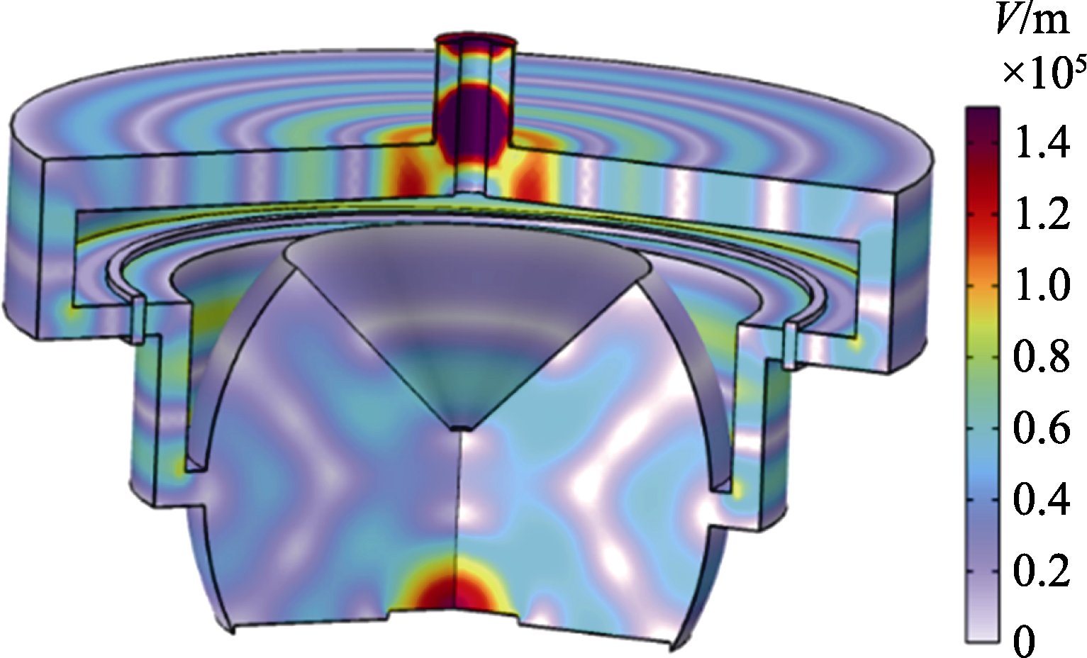
图1 MPCVD装置中微波电场的三维谐振模式图
Fig. 1 Three-dimensional resonance mode diagram of microwave electric field in MPCVD device
| Num. | Electron collision reaction | Collision type | Energy loss/eV |
|---|---|---|---|
| 1 | Elastic collision | - | |
| 2 | Excitation | 14 | |
| 3 | Dissociation | 8.9 | |
| 4 | Ionization | 15.4 |
表1 碰撞反应的集合[21]
Table 1 Set of collision reactions [21]
| Num. | Electron collision reaction | Collision type | Energy loss/eV |
|---|---|---|---|
| 1 | Elastic collision | - | |
| 2 | Excitation | 14 | |
| 3 | Dissociation | 8.9 | |
| 4 | Ionization | 15.4 |
| Num. | Surface reaction | Adhesion factor | Secondary emission coefficient |
|---|---|---|---|
| 1 | 1 | 0 | |
| 2 | 1 | 0 | |
| 3 | 1 | 0 |
表2 表面反应的集合
Table 2 Collection of surface reactions
| Num. | Surface reaction | Adhesion factor | Secondary emission coefficient |
|---|---|---|---|
| 1 | 1 | 0 | |
| 2 | 1 | 0 | |
| 3 | 1 | 0 |
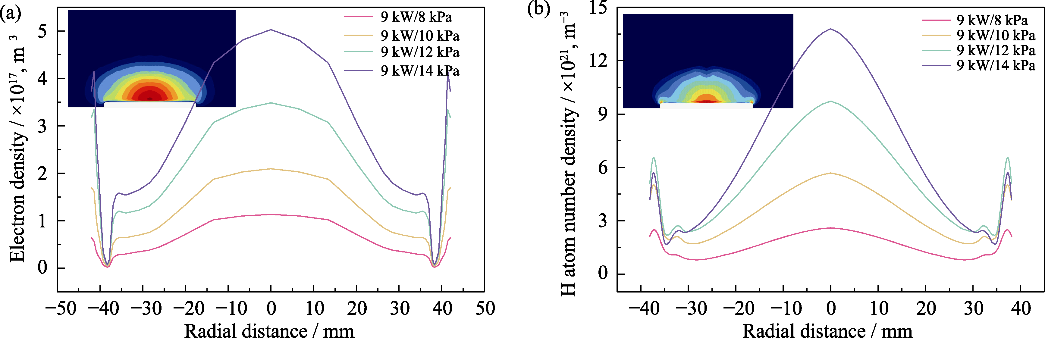
图2 不同微波功率/腔室压强条件下, 反应器轴线方向上的基团分布
Fig. 2 Group distribution in the axial direction of the reactor under different microwave power/chamber pressure conditions (a) Electron number density distribution; (b) Atomic H number density distribution
| Chamber pressure/kPa | ne/m−3 | nH/m−3 | ||
|---|---|---|---|---|
| r=0, z=0.5 | r=38.1, z=0.5 | r=0, z=0.5 | r=38.1, z=0.5 | |
| 6 | 1.14×10¹⁷ | 1.96×10¹⁵ | 2.83×10²¹ | 1.26×10²¹ |
| 8 | 2.09×10¹⁷ | 3.18×10¹⁵ | 6.00×10²¹ | 2.02×10²¹ |
| 10 | 3.44×10¹⁷ | 4.63×10¹⁵ | 1.05×10²² | 2.21×10²¹ |
| 12 | 4.97×10¹⁷ | 5.31×10¹⁵ | 1.51×10²² | 1.67×10²¹ |
表3 不同腔室压强下, 基片中心(r=0, z=0.5)与边缘(r=38.1, z=0.5)处的电子数密度ne和原子H数密度nH
Table 3 Electron number density ne and atomic H number density nH at the center (r=0, z=0.5) and edge (r=38.1, z=0.5) of the substrate under different chamber pressures
| Chamber pressure/kPa | ne/m−3 | nH/m−3 | ||
|---|---|---|---|---|
| r=0, z=0.5 | r=38.1, z=0.5 | r=0, z=0.5 | r=38.1, z=0.5 | |
| 6 | 1.14×10¹⁷ | 1.96×10¹⁵ | 2.83×10²¹ | 1.26×10²¹ |
| 8 | 2.09×10¹⁷ | 3.18×10¹⁵ | 6.00×10²¹ | 2.02×10²¹ |
| 10 | 3.44×10¹⁷ | 4.63×10¹⁵ | 1.05×10²² | 2.21×10²¹ |
| 12 | 4.97×10¹⁷ | 5.31×10¹⁵ | 1.51×10²² | 1.67×10²¹ |
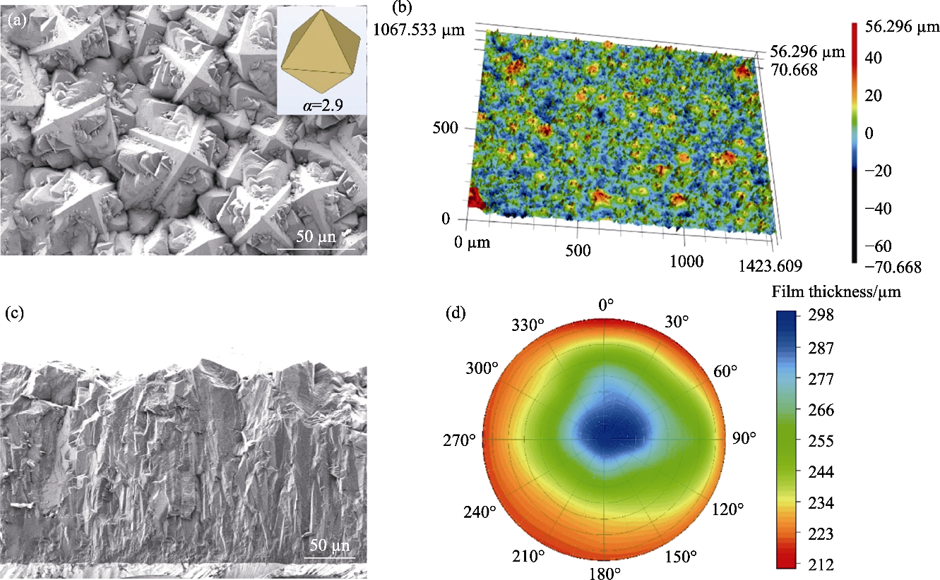
图3 金刚石薄膜的表面形貌、截面形貌及厚度分布
Fig. 3 Surface morphology, cross-sectional morphology and thickness distribution of the diamond film (a) Surface topography of a silicon substrate diamond film with inset illustrating the ideal diamond crystal profile when the growth parameter α is 2.9; (b) Surface profile of silicon substrate diamond film obtained by laser confocal microscope; (c) Cross-sectional morphology of the edge of the diamond film; (d) Thickness distribution of diamond film
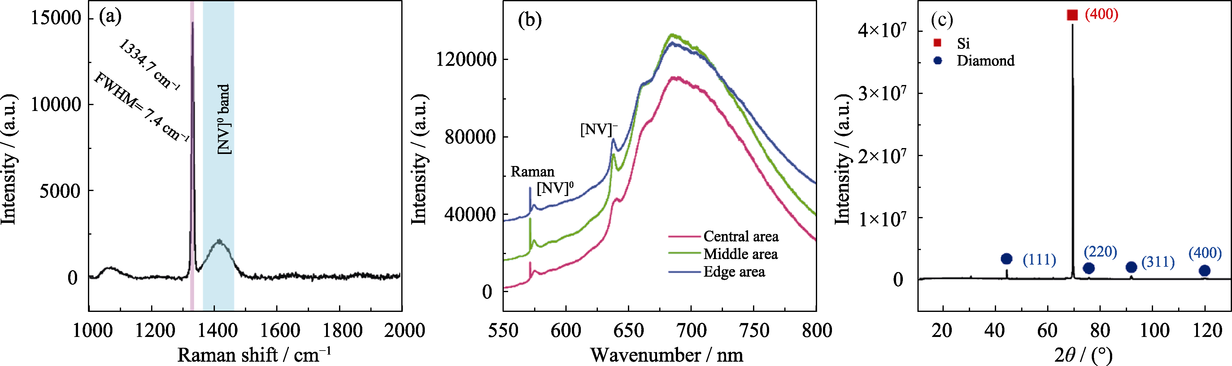
图4 硅衬底金刚石膜的Raman光谱(a)、PL光谱(b)及XRD图谱(c)
Fig. 4 Raman spectrum (a), PL spectra (b) and XRD pattern (c) of diamond films on silicon substrate
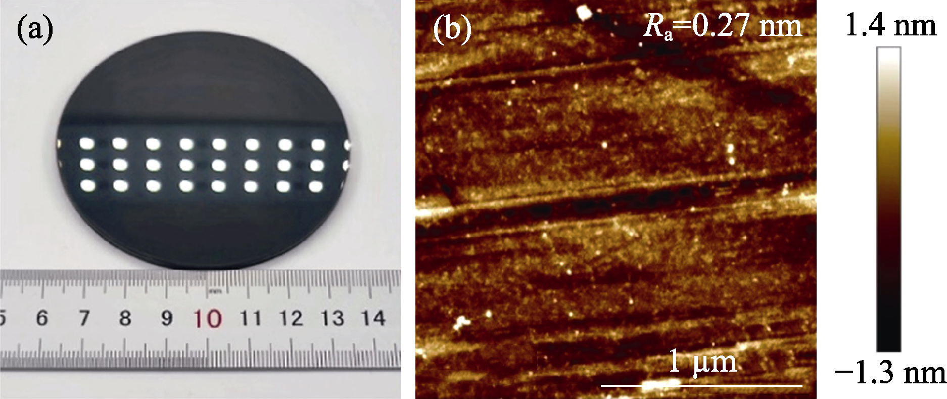
图5 抛光后的硅衬底金刚石膜的实物图及AFM表面形貌
Fig. 5 Actual photographic and AFM morphology of polished diamond films on silicon substrate (a) Actual photographic; (b) AFM image
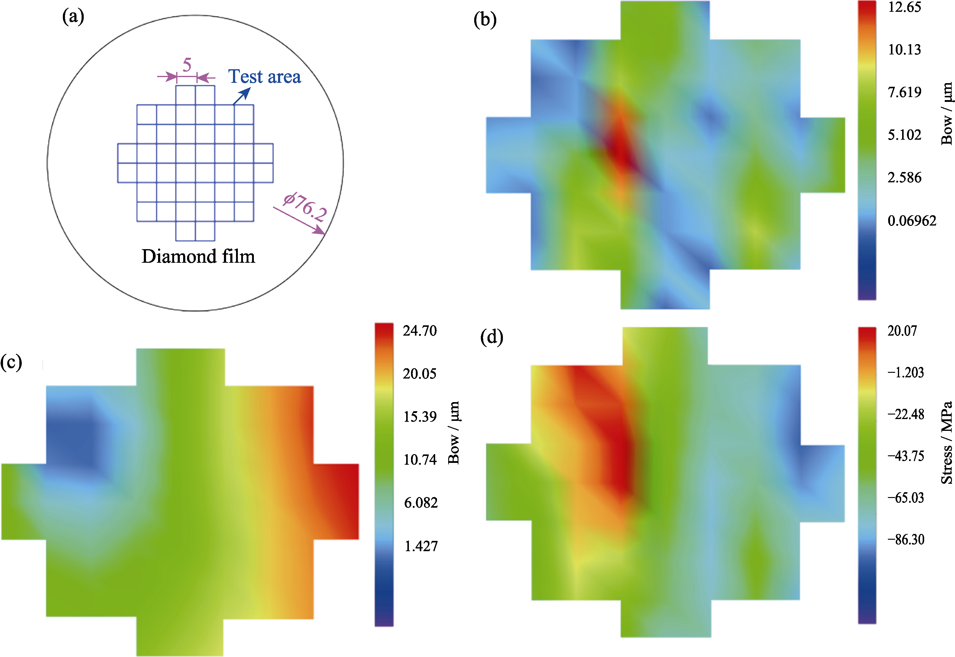
图6 薄膜弯曲度及应力测试结果
Fig. 6 Results of film bending and stress test (a) Test area of the film stress test system; (b) Bending test results of the monocrystalline silicon substrate; (c) Bending test results of the polished silicon substrate diamond film; (d) Internal stress of the diamond film calculated by the Stoney formula
| [1] |
PEARTON S J, REN F, ZHANG A P, et al. Fabrication and performance of GaN electronic devices. Mater. Sci. Engin.: R: Reports, 2000, 30(3-6): 55.
DOI URL |
| [2] | MAZUMDER S K, VOSS L F, DOWLING K, et al. Overview of wide/ultra-wide bandgap power semiconductor devices for distributed energy resources. IEEE J. Em. Sel. Top. P., 2023, 11(4): 3957. |
| [3] |
AJAYAN J, NIRMAL D, RAMESH R, et al. A critical review of AlGaN/GaN-heterostructure based Schottky diode/HEMT hydrogen (H2) sensors for aerospace and industrial applications. Measurement, 2021, 186: 110100.
DOI URL |
| [4] |
NUTTINCK S, GEBARA E, LASKAR J, et al. Study of self-heating effects, temperature-dependent modeling, and pulsed load- pull measurements on GaN HEMTs. IEEE T. Microw. Theory., 2001, 49(12): 2413.
DOI URL |
| [5] |
QIN Y, CHAI C, LI F, et al. Study of self-heating and high-power microwave effects for enhancement-mode p-gate GaN HEMT. Micromachines, 2022, 13(1): 106.
DOI URL |
| [6] |
CHEN J T, BERGSTEN J, LU J, et al. A GaN-SiC hybrid material for high-frequency and power electronics. Appl. Phys. Lett., 2018, 113(4): 041605.
DOI URL |
| [7] |
CHEN K J, HABERLEN O, LIDOW A, et al. GaN-on-Si power technology: devices and applications. IEEE T. Electron. Dev., 2017, 64(3): 779.
DOI URL |
| [8] |
MIZUE C, HORI Y, MICZEK M, et al. Capacitance-voltage characteristics of Al2O3/AlGaN/GaN structures and state density distribution at Al2O3/AlGaN interface. Jpn. J. Appl. Phys., 2011, 50(2R): 021001.
DOI |
| [9] |
LIU H, LI J, LI Z, et al. Single crystal diamond deposited by dual radio-frequency plasma jet CVD with high growth rate. Crystals, 2019, 9(1): 32.
DOI URL |
| [10] |
ZUO Y, LI J, BAI Y, et al. Growth of nanocrystalline diamond by dual radio frequency inductively coupled plasma jet CVD. Diam. Relat. Mater., 2017, 73: 67.
DOI URL |
| [11] | POMEROY J, BERNARDONI M, SARUA A, et al. Achieving the best thermal performance for GaN-on-diamond. 2013 IEEE Compound Semiconductor Integrated Circuit Symposium (CSICS), 2013, 1: 6659210. |
| [12] | ZHAO J, HAO X, ZHAO K, et al. Recent development on high thermal conductivity diamond synthesized by microwave plasma chemical vapor deposition and its devices applications. J. Chin. Ceram. Soc., 2022, 50(7): 1852. |
| [13] |
GROTJOHN T, LISKE R, HASSOUNI K, et al. Scaling behavior of microwave reactors and discharge size for diamond deposition. Diam. Relat. Mater., 2005, 14(3-7): 288.
DOI URL |
| [14] |
SILVA F, BONNIN X, SCHARPF J, et al. Microwave analysis of PACVD diamond deposition reactor based on electromagnetic modelling. Diam. Relat. Mater., 2010, 19(5/6): 397.
DOI URL |
| [15] |
LI Y F, SU J J, LIU Y Q, et al. A circumferential antenna ellipsoidal cavity type MPCVD reactor developed for diamond film deposition. Diam. Relat. Mater., 2015, 51: 24.
DOI URL |
| [16] |
AN K, ZHANG S, SHAO S, et al. Effects of the electric field at the edge of a substrate to deposit a ϕ100 mm uniform diamond film in a 2.45 GHz MPCVD system. Plasma Sci. Technol., 2022, 24(4): 045502.
DOI |
| [17] |
WENG J, LIU F, XIONG L W, et al. Deposition of large area uniform diamond films by microwave plasma CVD. Vacuum, 2018, 147: 134.
DOI URL |
| [18] |
LI Y C, LIU X D, HAO X B, et al. Rapid growth of single crystal diamond at high energy density by plasma focusing. J. Inorg. Mater., 2023, 38(3): 303.
DOI |
| [19] |
YAMADA H, CHAYAHARA A, MOKUNO Y. Simplified description of microwave plasma discharge for chemical vapor deposition of diamond. J. Appl. Phys., 2007, 101(6): 063302.
DOI URL |
| [20] |
SU J J, LI Y F, LI X L, et al. A novel microwave plasma reactor with a unique structure for chemical vapor deposition of diamond films. Diam. Relat. Mater., 2014, 42: 28.
DOI URL |
| [21] | Itikawa database. www.lxcat.net.(2022-04-10)[2023-11-08]. |
| [22] |
YANG D, GUO L, WANG B, et al. Hydrogen plasma characteristics in a microwave chemical vapor deposition chamber. Mater. Sci. Eng. B-Adv., 2023, 292: 116422.
DOI URL |
| [23] |
MESBAHI A, SILVA F, FARHAT S, et al. Hydrodynamics effects in high power density microwave plasma diamond growth reactors. J. Phys. D Appl. Phys., 2013, 46(38): 385502.
DOI URL |
| [24] | ZHANG S, AN K, SHAO S W, et al. Microwave power and deposition pressure matching of MPCVD diamond films. J. Synth. Cryst., 2022, 51(5): 910. |
| [25] |
WILD C, KOIDL P, MULLER-SEBERT W, et al. Chemical vapour deposition and characterization of smooth {100}-faceted diamond films. Diam. Relat. Mater., 1993, 2(2/3/4): 158.
DOI URL |
| [26] | ZHU H X, WU S, HUANG L L, et al. Effect of methane concentration on twins in CVD polycrystalline diamond film. Physics Examination and Testing, 2014, 32(1): 7. |
| [27] | MAO W M, ZHU H X, CHEN L, et al. Macro-texture and micro-twinning in CVD free-standing diamond films. J. Inorg. Mater., 2006, 21(1): 239. |
| [28] |
LEIGH W G S, CUENCA J A, THOMAS E L H, et al. Mapping the effect of substrate temperature inhomogeneity during microwave plasma-enhanced chemical vapour deposition nanocrystalline diamond growth. Carbon, 2023, 201: 328.
DOI URL |
| [29] |
HUAMH Y, ROSAKIS A J. Extension of Stoney's formula to non-uniform temperature distributions in thin film/substrate systems. The case of radial symmetry. J. Mech. Phys. Solids., 2005, 53(11): 2483.
DOI URL |
| [30] | NAKAMURA Y, SAKAGAMI S, AMAMOTO Y, et al. Measurement of internal stresses in CVD diamond films. Thin Solid Films, 1997, 308: 249. |
| [31] |
LI X, LI C, GAO C, et al. Internal stress in MPCVD diamond films on the Si substrate based on XRD line shape. Optoelectron. Lett., 2009, 5(4): 273.
DOI URL |
| [32] |
LI H Y, KUANG F H, WU H L, et al. Temperature dependence of residual tensile stresses and its influences on crack propagation behaviour. J. Inorg. Mater., 2023, 38(11): 1265.
DOI URL |
| [1] | 赵志翰, 郭鹏, 魏菁, 崔丽, 刘山泽, 张文龙, 陈仁德, 汪爱英. Ti-DLC薄膜压阻性能及载流子输运行为研究[J]. 无机材料学报, 2024, 39(8): 879-886. |
| [2] | 李一村, 刘雪冬, 郝晓斌, 代兵, 吕继磊, 朱嘉琦. 等离子体聚集装置下的高能量密度单晶金刚石快速生长研究[J]. 无机材料学报, 2023, 38(3): 303-309. |
| [3] | 李一村, 郝晓斌, 代兵, 文东岳, 朱嘉琦, 耿方娟, 乐卫平, 林伟群. 基于等离子体诊断的MPCVD单晶金刚石生长优化设计[J]. 无机材料学报, 2023, 38(12): 1405-1412. |
| [4] | 姜金龙, 王 琼, 黄 浩, 张 霞, 王玉宝, 耿庆芬. 紫外光辐照下钛硅共掺杂类金刚石薄膜微结构的演化[J]. 无机材料学报, 2014, 29(9): 941-946. |
| [5] | 刘金龙, 李成明, 陈良贤, 黑立富, 吕反修. 高频大功率金刚石薄膜场效应管的研究进展[J]. 无机材料学报, 2010, 25(9): 897-905. |
| [6] | 李红凯, 林国强, 董 闯. 脉冲偏压电弧离子镀制备C1-x-yNxZry超硬复合薄膜[J]. 无机材料学报, 2010, 25(5): 517-521. |
| [7] | 沈沪江,王林军,黄 健,徐 闰,史伟民,夏义本. 基于(100)定向金刚石薄膜的辐射探测器研究[J]. 无机材料学报, 2009, 24(6): 1254-1258. |
| [8] | 朱嘉琦,卢 佳,田 桂,檀满林,耿 达. 非晶硅太阳电池窗口层材料掺硼非晶金刚石的研究[J]. 无机材料学报, 2008, 23(5): 1064-1066. |
| [9] | 朱宏喜,毛卫民,冯惠平,吕反修,Vlasov I I,Ralchenko V G,Khomich A V. 甲烷浓度对CVD金刚石薄膜晶体学生长过程的影响[J]. 无机材料学报, 2007, 22(3): 570-576. |
| [10] | 吴南春,夏义本,谭寿洪,刘健敏,苏青峰,王林军. 正偏压对纳米金刚石薄膜结构和电阻率的影响[J]. 无机材料学报, 2007, 22(2): 381-384. |
| [11] | 刘健敏,夏义本,王林军,张明龙,苏青峰. 工艺条件对热丝 CVD金刚石薄膜电学性能的影响[J]. 无机材料学报, 2006, 21(4): 1018-1024. |
| [12] | 苏青峰,夏义本,王林军,史伟民. 复合抛光对 CVD金刚石薄膜表面光洁度的改进研究[J]. 无机材料学报, 2006, 21(2): 499-502. |
| [13] | 刘卫平,余庆选,田宇全,廖源,王冠中,方容川. 硼掺杂对金刚石薄膜生长特性的影响[J]. 无机材料学报, 2005, 20(5): 1270-1274. |
| [14] | 林良武,唐元洪,朱利兵. 原子氢在纳米金刚石薄膜生长中的作用[J]. 无机材料学报, 2005, 20(5): 1263-1269. |
| [15] | 蒋娜娜,邵天敏,陈大融. 利用脉冲激光真空弧沉积技术制备类金刚石薄膜[J]. 无机材料学报, 2005, 20(1): 187-192. |
| 阅读次数 | ||||||
|
全文 |
|
|||||
|
摘要 |
|
|||||