Journal of Inorganic Materials ›› 2012, Vol. 27 ›› Issue (5): 449-457.DOI: 10.3724/SP.J.1077.2012.00449
• Orginal Article • Next Articles
CHEN Chang-Xin, JIN Tie-Ning, ZHANG Ya-Fei
Received:2011-09-12
Revised:2011-11-29
Published:2012-05-10
Online:2012-03-31
Supported by:CLC Number:
CHEN Chang-Xin, JIN Tie-Ning, ZHANG Ya-Fei. Progress in Improvement Methods of Carbon Nanotube/Metal Contact[J]. Journal of Inorganic Materials, 2012, 27(5): 449-457.
Add to citation manager EndNote|Ris|BibTeX

Fig. 1 (a) HRTEM image of the contact interface of TiC and SWCNT bundle after annealing[2]; (b) I-V curves of a SWCNT bridging two Ti pads (as illustrated in the inset) before and after annealing[2]

Fig. 2 Evolution of the XRD of a titanium film covering SWCNTs dispersed on a SiO2/Si substrate as a function of temperature[4]
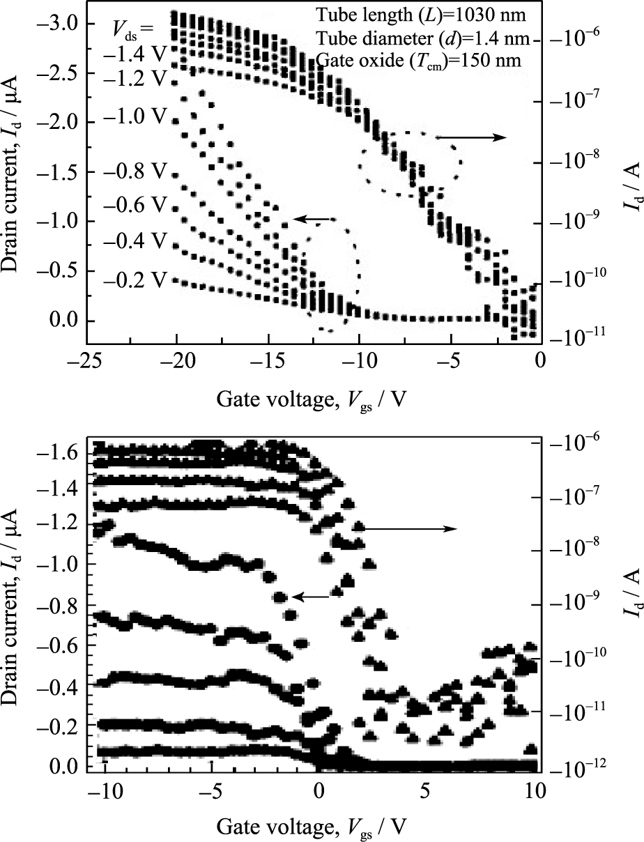
Fig. 3 Id-Vgs curves of the Co contacted CNTFET (a) and the Ti contacted CNTFET (b); The right curves in the figures are the logarithmic plot of Id-Vgs characteristics[3]
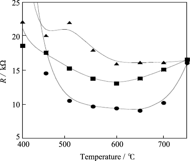
Fig. 4 Contact resistance as a function of the rapid thermal annealing (RTA) tem-perature for three different nanotube–Ti–Au electrodes[7]

Fig. 5 A schematic diagram of the apparatus for the local CNT/electrode contact treatment using an electrical pulse shot[15]
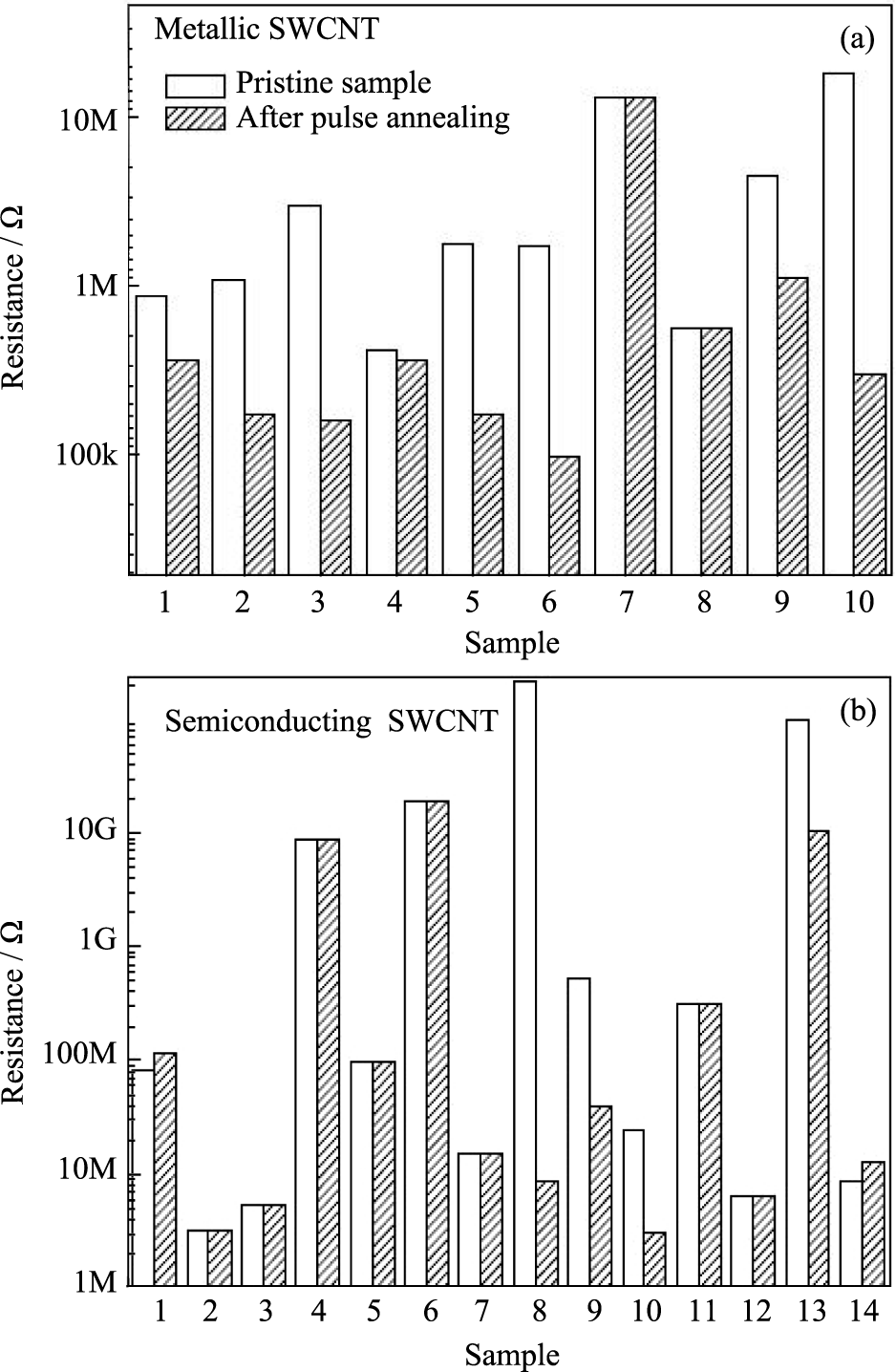
Fig. 6 Statistics of the changes in the 2-terminal resistance before (blank) and after (shadow) pulse annealing for the cases of an individual (a) metallic SWCNT and (b) semiconducting SWCNT[15]
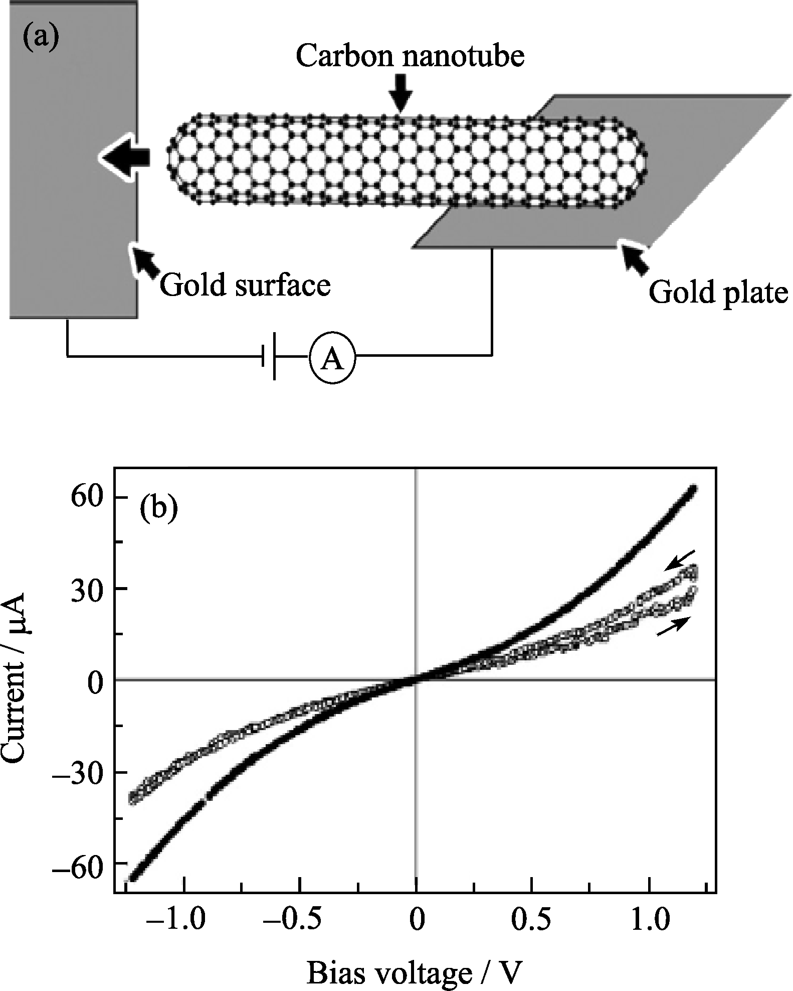
Fig. 7 (a) Illustration of the procedure for connecting a carbon nanotube to a gold surface[16]; (b) Current-voltage curves for two different contact states: open circles are data obtained when the MWCNT tip is just in contact with the gold surface and filled circles are for when the tip is embedded in the gold surface[16]

Fig. 8 (a) Schematic diagram of the process of electron beam deposition; (b) Current vs deposition time during soldering of the MWCNT using the electron beam[26]
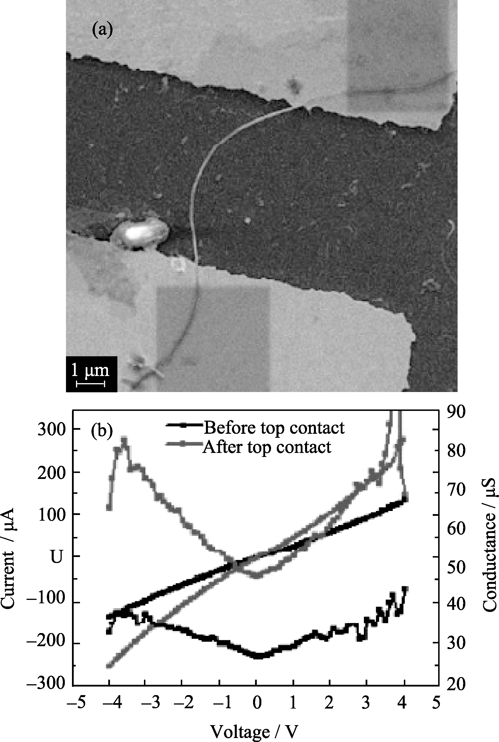
Fig. 9 (a) The SEM image of the contacts of CNT and gold pads after top metal deposition; (b) The I-V and G-V curves before (black) and after (gray) the electron beam deposition[27]
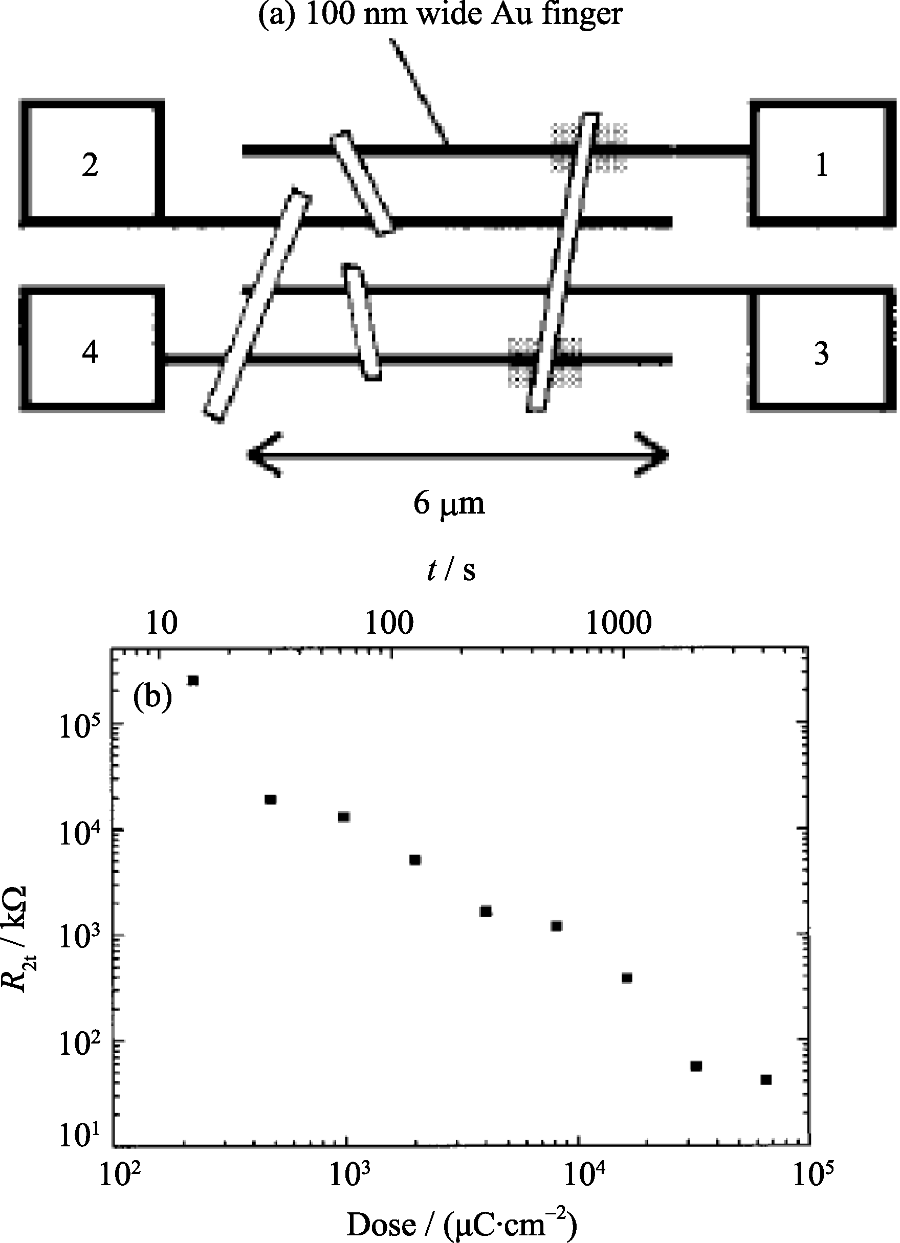
Fig. 10 (a) Schematic of exposing the CNT/Au contacts under electron beam. The shadows show the areas of electron beam irritation[29]; (b) Two-terminal resistance R2t as a function of electron exposure dose in SEM[29]
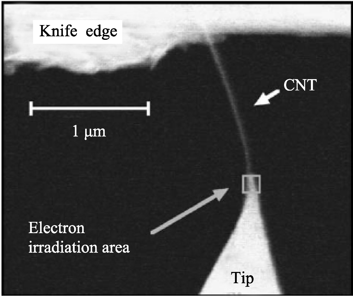
Fig. 11 SEM image of the contact between CNT and metal Pt on Si cantilever surface after electron beam irradiation[30]
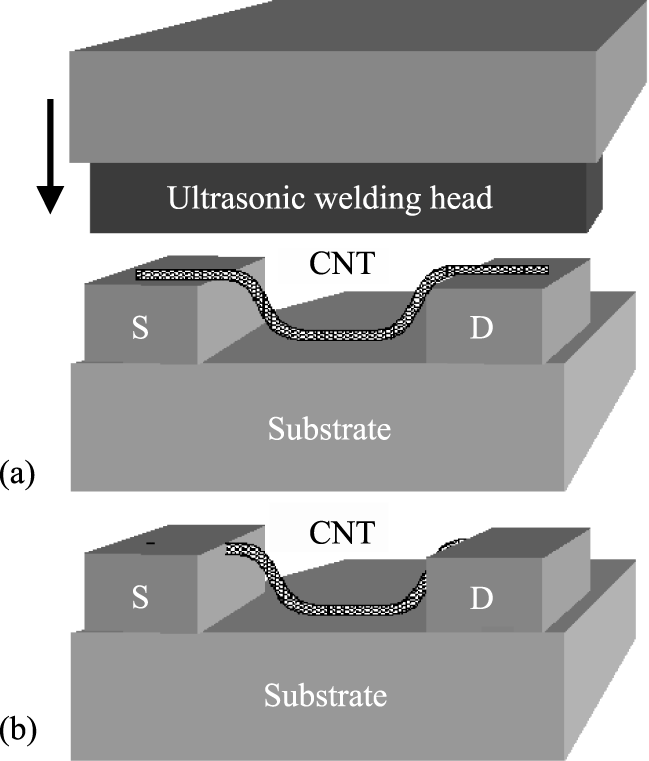
Fig. 12 Schematic diagrams of the ultrasonic nanowelding process[32] (a) Before welding; (b) After welding
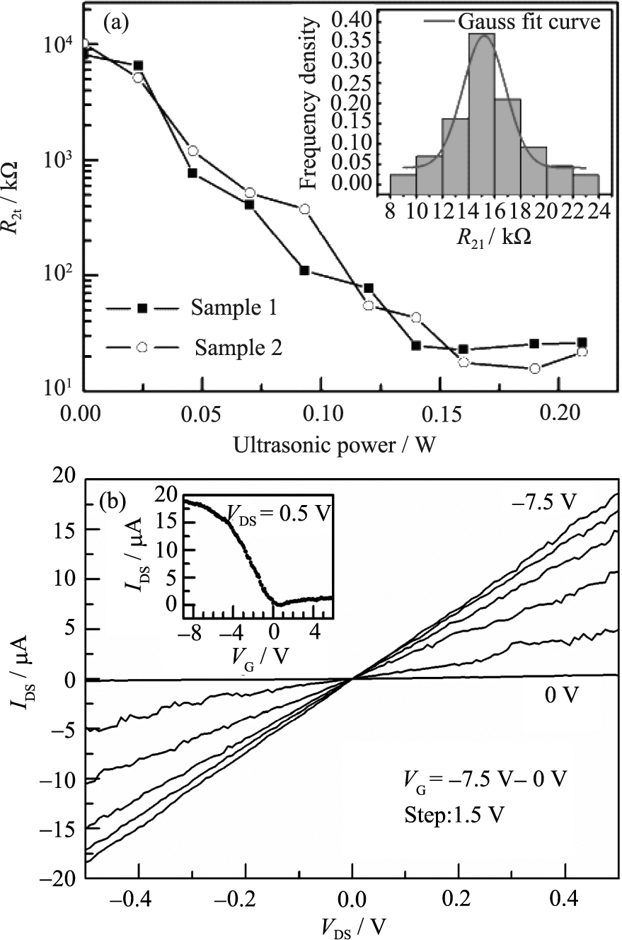
Fig. 13 (a) Two-terminal (2t-) resistance as a function of the ultrasonic power for two metallic nanotube; Inset: the statistical analysis and distribution fit of the obtained lowest 2t-resistances for 43 samples after nanowelding, which indicates that the lowest resistance is about 15 kΩ[32]; (b) Output characteristic of the fabricated CNTFET. Inset: transfer characteristic curve[32]
| [1] | Avouris P, Hertel T, Martel R, et al. Carbon nanotubes nanomechanics, manipulation, and electronic devices. Applied Surface Science, 1999, 141(3/4): 201-209. |
| [2] | Zhang Y, Ichihashi T, Landree E, et al. Heterostructrues of single-walled carbon nanotubes and carbide nanorods. Science, 1999, 285(5434): 1719-1720. |
| [3] | Martel R, Wong H S P, Chan K, et al. Carbon Nanotube Field Effect Transistors for Logic Application. IEDM Technical Digest, 2001: 159-162. |
| [4] | Martel R, Derycke V, Lavoie C, et al. Ambipolar electrical transport in semiconducting single-wall carbon nanotubes. Physical Review Letters, 2001, 87(25): 256805-1-4. |
| [5] | Avouris P, Appenzeller J, Martel R, et al. Carbon nanotube electronics. Proceedings of IEEE, 2003, 91(11): 1772-1784. |
| [6] | Avouris P, Martel R, Derycke V, et al. Carbon nanotube transistors and logic circuits. Physica B, 2003, 323(1-4): 6-14. |
| [7] | Lee J O, Park C, Kim J J, et al. Formation of low-resistance ohmic contacts between carbon nanotube and metal electrodes by a rapid thermal annealing method. Journal of Physics D:Applied Physics, 2000, 33(16):1953-1956. |
| [8] | Kane A, Sheps T, Branigan E, et al. Contacts to metallic single-walled carbon nanotubes using Pt electrodes. Nano Letters, 2009, 9(10): 3586-3591. |
| [9] | Bhuvana T, Smith K, Fisher T, et al. Self-assembled CNT circuits with ohmic contacts using Pd hexadecanethiolate as in situ solder. Nanoscale, 2009, 1(2): 271-275. |
| [10] | Roschier L, Tarkiainen R, Ahlskog M. Manufacture of single electron transistors using AFM manipulation on multiwalled carbon nanotubes. Microelectronic Engineering, 2002, 61-62: 687-691. |
| [11] | Huang L, Chor E F, Wu Y, et al. Investigations of niobium carbide contact for carbon-nanotube-based devices. Nanotechnology, 2010, 21(9): 095201. |
| [12] | Tan M M, Ye X Y, Wang X H, et al. Improving contact of CNT-metal by annealing. Journal of Functional Materials and Devices, 2008, 14(1): 227-230. |
| [13] | Hobara R, Yoshimoto S, Ikuno T, et al. Electronic transport in mutiwalled carbon nanotubes contacted with patterned electrodes. Japanese Journal of Applied Physics, 2004, 43(8B): 1081-1084. |
| [14] | Hsiou Y, Yang Y J, Stobinski L, et al. On the Ohmic contact between multiwalled carbon nanotubes and nano-electrodes. Chinese Journal of Physics, 2005, 43(1-II): 293-297. |
| [15] | Woo Y S, Duseberg G, Roth S. Reduced contact resistance between an individual single-walled carbon nanotube and a metal electrode by a local point annealing. Nanotechnology, 2007, 18(9): 095203-1-3. |
| [16] | Asaka K, Karita M, Saito Y. Modification of interface structure and contact resistance between a carbon nanotube and a gold electrode by local melting. Applied Surface Science, 2011, 257(7): 2850-2853. |
| [17] | Dong L F, Youkey S, Bush J, et al. Effect of local joule heating on the reduction contact resistance between carbon nanotubes and metal electrodes. Journal of Applied Physics, 2007, 101(2): 024320-1-7. |
| [18] | Tian X J, Wang Y C, Dong Z L. A Study on the assembly and improovement of electrical contact between carbon nanotube and microelectrode. Advanced Materials Research, 2009, 60-61: 399-405. |
| [19] | Maki H, Masaki S, Ishibashi J. Local change of carbon nanotube- metal contacts by current flow through electrodes. Japanese Journal of Applied Physics, 2004, 43(4B) : 2027-2030. |
| [20] | Yamada T, Saito T, Suzuki M, et al. Tunneling between carbon nanofiber and gold electrodes. Journal of Applied Physics, 2010, 107(4) : 044304-1-5. |
| [21] | Dong L F, Chirayos V, Bush J, et al. Floating-potential dielectrophoresis-controlled fabrication of single-carbon-nanotube transistors and their electrical properties. Journal of Physics Chemisty B, 2005, 109(27) : 13148-13153. |
| [22] | Woo Y S, Roth S. Effect of Contact Improvement on the FET Characteristics of an Individual Single Walled Carbon Nanotube. AIP Conference Proceeding, 2005, 786: 566-569. |
| [23] | Tsutsui M, Taninouchi Y, Kurokawa S, et al. Bias-induced local heating effects on multi-walled carbon nanotube-Au contacts. Japanese Journal of Applied Physics, 2006, 45(1A): 341-345. |
| [24] | Wang M S, Golberg D, Bando Y. Superstrong low-resistant carbon nanotube-carbide-metal nanocontacts. Advanced Materials, 2010, 22(47): 5350-5355. |
| [25] | Chen Q, Wang S, Peng L M. Establishing Ohmic contacts for in situ current-voltage characteristic measurements on a carbon nanotube inside the scanning electron microscope. Nanotechnology, 2006, 17(4): 1087-1098. |
| [26] | Madsen D N, Molhave K, Mateiu R, et al. Solding of nanotubes onto microelectrodes. Nano Letters, 2003, 3(1): 47-49. |
| [27] | Neha K, Misra A, Srinivasan S, et al. Effect of top metal contact on electrical transport through individual multiwalled carbon nanotube. Applied Physics Letters, 2010, 97(22): 222102-1-3. |
| [28] | Tersoff J. Contact resistance of carbon nanotubes. Applied Physics Letters, 1999, 74(15): 2122-2124. |
| [29] | Bachtold A, Henny M, Terrier C, et al. Contacting carbon nanotubes selectively with low-ohmic contacts for four-probe electric measurements. Applied Physics Letters, 1998, 73(2): 274-276. |
| [30] | Ando A, Shimizu T, Abe H, et al. Improvement of electrical contact at carbon nanotube/Pt by selective electron irradiation. Physica E, 2004, 24(1/2): 6-9. |
| [31] | Rodriguez-Manzo J, Banhart F, Terrones M, et al. Heterojunctions between metals and carbon nanotubes as ultimate nanocontacts. Applied Physical Science, 2009, 106(12): 4591-4595. |
| [32] | Chen C X, Yan L J, Kong E S, et al. Ultrasonic nanowelding of carbon nanotubes to metal electrodes. Nanotechnology, 2006, 17(9): 2192-2197. |
| [33] | Chen C X, Liu L Y, Lu Y, et al. A method for creating reliable and low-resistance contacts between carbon nanotubes and microelectrodes. Carbon, 2007, 45(2): 436-442. |
| [34] | Chen C X, Xu D, Kong E S, et al. Multichannel carbon-nanotube FETs and complementary logic gates with nanowelded contacts. IEEE Electron Device Letters, 2006, 27(10): 852-855. |
| [35] | Chen C X, Zhang W, Zhang Y F. Multichannel carbon nanotube field-effect transistors with compound channellayer. Applied Physics Letters, 2009, 95(19): 192110-1-3. |
| [36] | Chen C X, Lu Y, Kong E S, et al. Nanowelded carbon-nanotube- based solar microcells. Small, 2008, 4(9): 1313-1318. |
| [37] | Chen C X, Zhang W, Kong E S, et al. Carbon nanotube photovoltaic device with asymmetrical contacts. Appllied Physics Letters, 2009, 94(26): 263501-1-3. |
| [38] | Lim S C, Jang J H, Bae D J, et al. Contact resistance between metal and carbon nanotube interconnects:effect of work function and wettability. Applied Physics Letters, 2009, 95(26): 264103-1-3. |
| [39] | Song Y J, Kang S J. Improvement of contact resistance between carbon nanotubes and metal electrodes for high performance electronics. J. Vac. Sci. Technol. B, 2010, 29(1): 011011-1-3. |
| [40] | Nirmalraj P N, Boland J J. Selective tuning and optimization of the contacts to metallic and semiconducting single-walled carbon nanotubes. ACS Nano, 2010, 4(7): 3801-3806. |
| [41] | Dockendorf C, Steinlin M, Proulikakos D. Individual carbon nanotube soldering with gold nanoink deposition. Applied Physics Letters, 2007, 90(19): 193116-1-3. |
| [42] | Lee S, Park J Y, Cho Y S, et al. Nanosoldering of carbon nanotubes on metal electrodes with an atomic force microscope. Journal of Vacuum Science and Technology B, 2007, 25(3): 916-1-6. |
| [43] | Liebau M, Unger E, Duesberg G, et al. Contact improvement of carbon nanotubes via electroless nickel deposition. Applied Physics A, 2003, 77(6): 731-734. |
| [44] | Seidel R, Liebau M, Duesberg G.et al. In-situ contacted single- walled carbon nanotubes and contact improvement by electroless deposition. Nano Letters, 2003, 3(7): 965-968. |
| [45] | Leon J, Flacker A, Vaz A, et al. Electrical characterization of multi-walled carbon nanotubes. Journal of Nanoscience andNanotechnology, 2010, 10(9): 6234-6239. |
| [46] | Caillier C, Ayan A, Gouttenoire V, et al. Gold contact to individual metallic carbon nanotubes: asensitive nanosensor for high-pressure. Applied Physics Letters, 2010, 97(17): 173111-1-3. |
| [47] | Kasumov A, Deblock R, Kociak M, et al. Supercurrents through single-walled carbon nanotubes. Science, 1999, 284(5419): 1508-1510. |
| [1] | ZHU Wenjie, TANG Lu, LU Jichang, LIU Jiangping, LUO Yongming. Research Progress on Catalytic Oxidation of Volatile Organic Compounds by Perovskite Oxides [J]. Journal of Inorganic Materials, 2025, 40(7): 735-746. |
| [2] | HU Zhichao, YANG Hongyu, YANG Hongcheng, SUN Chengli, YANG Jun, LI Enzhu. Usage of the P-V-L Bond Theory in Regulating Properties of Microwave Dielectric Ceramics [J]. Journal of Inorganic Materials, 2025, 40(6): 609-626. |
| [3] | WU Qiong, SHEN Binglin, ZHANG Maohua, YAO Fangzhou, XING Zhipeng, WANG Ke. Research Progress on Lead-based Textured Piezoelectric Ceramics [J]. Journal of Inorganic Materials, 2025, 40(6): 563-574. |
| [4] | ZHANG Bihui, LIU Xiaoqiang, CHEN Xiangming. Recent Progress of Hybrid Improper Ferroelectrics with Ruddlesden-Popper Structure [J]. Journal of Inorganic Materials, 2025, 40(6): 587-608. |
| [5] | WU Jie, YANG Shuai, WANG Mingwen, LI Jinglei, LI Chunchun, LI Fei. Textured PT-based Piezoelectric Ceramics: Development, Status and Challenge [J]. Journal of Inorganic Materials, 2025, 40(6): 575-586. |
| [6] | JIANG Kun, LI Letian, ZHENG Mupeng, HU Yongming, PAN Qinxue, WU Chaofeng, WANG Ke. Research Progress on Low-temperature Sintering of PZT Ceramics [J]. Journal of Inorganic Materials, 2025, 40(6): 627-638. |
| [7] | TIAN Ruizhi, LAN Zhengyi, YIN Jie, HAO Nanjing, CHEN Hangrong, MA Ming. Microfluidic Technology Based Synthesis of Inorganic Nano-biomaterials: Principles and Progress [J]. Journal of Inorganic Materials, 2025, 40(4): 337-347. |
| [8] | ZHANG Jiguo, WU Tian, ZHAO Xu, YANG Fan, XIA Tian, SUN Shien. Improvement of Cycling Stability of Cathode Materials and Industrialization Process for Sodium-ion Batteries [J]. Journal of Inorganic Materials, 2025, 40(4): 348-362. |
| [9] | YIN Jie, GENG Jiayi, WANG Kanglong, CHEN Zhongming, LIU Xuejian, HUANG Zhengren. Recent Advances in 3D Printing and Densification of SiC Ceramics [J]. Journal of Inorganic Materials, 2025, 40(3): 245-255. |
| [10] | CHEN Guangchang, DUAN Xiaoming, ZHU Jinrong, GONG Qing, CAI Delong, LI Yuhang, YANG Donglei, CHEN Biao, LI Xinmin, DENG Xudong, YU Jin, LIU Boya, HE Peigang, JIA Dechang, ZHOU Yu. Advanced Ceramic Materials in Helicopter Special Structures: Research Progress and Application Prospect [J]. Journal of Inorganic Materials, 2025, 40(3): 225-244. |
| [11] | FAN Xiaobo, ZU Mei, YANG Xiangfei, SONG Ce, CHEN Chen, WANG Zi, LUO Wenhua, CHENG Haifeng. Research Progress on Proton-regulated Electrochemical Ionic Synapses [J]. Journal of Inorganic Materials, 2025, 40(3): 256-270. |
| [12] | HAIREGU Tuxun, GUO Le, DING Jiayi, ZHOU Jiaqi, ZHANG Xueliang, NUERNISHA Alifu. Research Progress of Optical Bioimaging Technology Assisted by Upconversion Fluorescence Probes in Tumor Imaging [J]. Journal of Inorganic Materials, 2025, 40(2): 145-158. |
| [13] | SUN Shujuan, ZHENG Nannan, PAN Haokun, MA Meng, CHEN Jun, HUANG Xiubing. Research Progress on Preparation Methods of Single-atom Catalysts [J]. Journal of Inorganic Materials, 2025, 40(2): 113-127. |
| [14] | TAO Guilong, ZHI Guowei, LUO Tianyou, OUYANG Peidong, YI Xinyan, LI Guoqiang. Progress on Key Technologies of Cavity-structured Thin Film Bulk Acoustic Wave Filter [J]. Journal of Inorganic Materials, 2025, 40(2): 128-144. |
| [15] | ZHOU Fan, TIAN Zhilin, LI Bin. Research Progress on Carbide Ultra-high Temperature Ceramic Anti-ablation Coatings for Thermal Protection System [J]. Journal of Inorganic Materials, 2025, 40(1): 1-16. |
| Viewed | ||||||
|
Full text |
|
|||||
|
Abstract |
|
|||||