无机材料学报 ›› 2026, Vol. 41 ›› Issue (6): 795-804.DOI: 10.15541/jim20250459
孙丽1( ), 徐永善2, 高义华1()
收稿日期:2025-11-18
修回日期:2025-12-31
出版日期:2026-06-20
网络出版日期:2026-01-22
通讯作者:
高义华, 教授. E-mail: gaoyihua@hust.edu.cn作者简介:孙 丽(1994-), 女, 博士. E-mail: Sunl_qdu@163.com
基金资助:
SUN Li1(), XU Yongshan2, GAO Yihua1()
Received:2025-11-18
Revised:2025-12-31
Published:2026-06-20
Online:2026-01-22
Contact:
GAO Yihua, professor. E-mail: gaoyihua@hust.edu.cnAbout author:SUN Li (1994-), female, PhD. E-mail: Sunl_qdu@163.com
Supported by:摘要:
随着电子器件朝着微型化、集成化与多功能智能化方向发展, 二维材料凭借其丰富的结构及独特的物理化学性质为该领域开辟了全新的发展路径。其中, Bi2O2Se因其适宜的带隙、高载流子迁移率及良好的环境稳定性而受到广泛关注。然而, 目前Bi2O2Se基器件仍存在暗电流大、响应度低等问题, 制约了其在高性能光电器件领域的进一步发展。本研究采用化学气相沉积工艺在云母衬底上可控生长了高质量二维Bi2O2Se纳米片, 并首次采用对称石墨烯(Gr)作为接触电极构建了Gr/Bi2O2Se/Gr对称双异质结器件。该结构利用Gr与Bi2O2Se之间形成的双界面内建电场, 优化了载流子的注入与分离过程。系统表征了该器件在黑暗及不同波长光照下的电流-电压特性、时间响应特性及光谱响应范围, 并深入探究了器件在脉冲光刺激下的动态电学行为, 模拟了生物突触的短期与长期可塑性功能。研究表明, 在532 nm光照下, 器件展现出良好的响应度(2.52 A/W)和探测率(3.39×109 Jones), 且在宽波长范围(365~1050 nm)内具有稳定的光响应, 证明了其作为宽带光探测器的潜力。在365 nm脉冲刺激下, 该器件展现出从短时程可塑性到长时程可塑性的转变, 通过调节光脉冲的强度、频率和数量, 精确模拟了包括兴奋性突触后电流、尖峰时序依赖可塑性在内的核心生物突触行为。此外, 该器件还成功复现了“经验学习”这一特征, 充分证明了其在神经形态计算领域的潜力。
中图分类号:
孙丽, 徐永善, 高义华. 石墨烯/Bi2O2Se/石墨烯双异质结器件的光探测和仿生突触研究[J]. 无机材料学报, 2026, 41(6): 795-804.
SUN Li, XU Yongshan, GAO Yihua. Photonic-detection and Bionic-synapse of Graphene/Bi2O2Se/Graphene Bi-heterojunction Device[J]. Journal of Inorganic Materials, 2026, 41(6): 795-804.
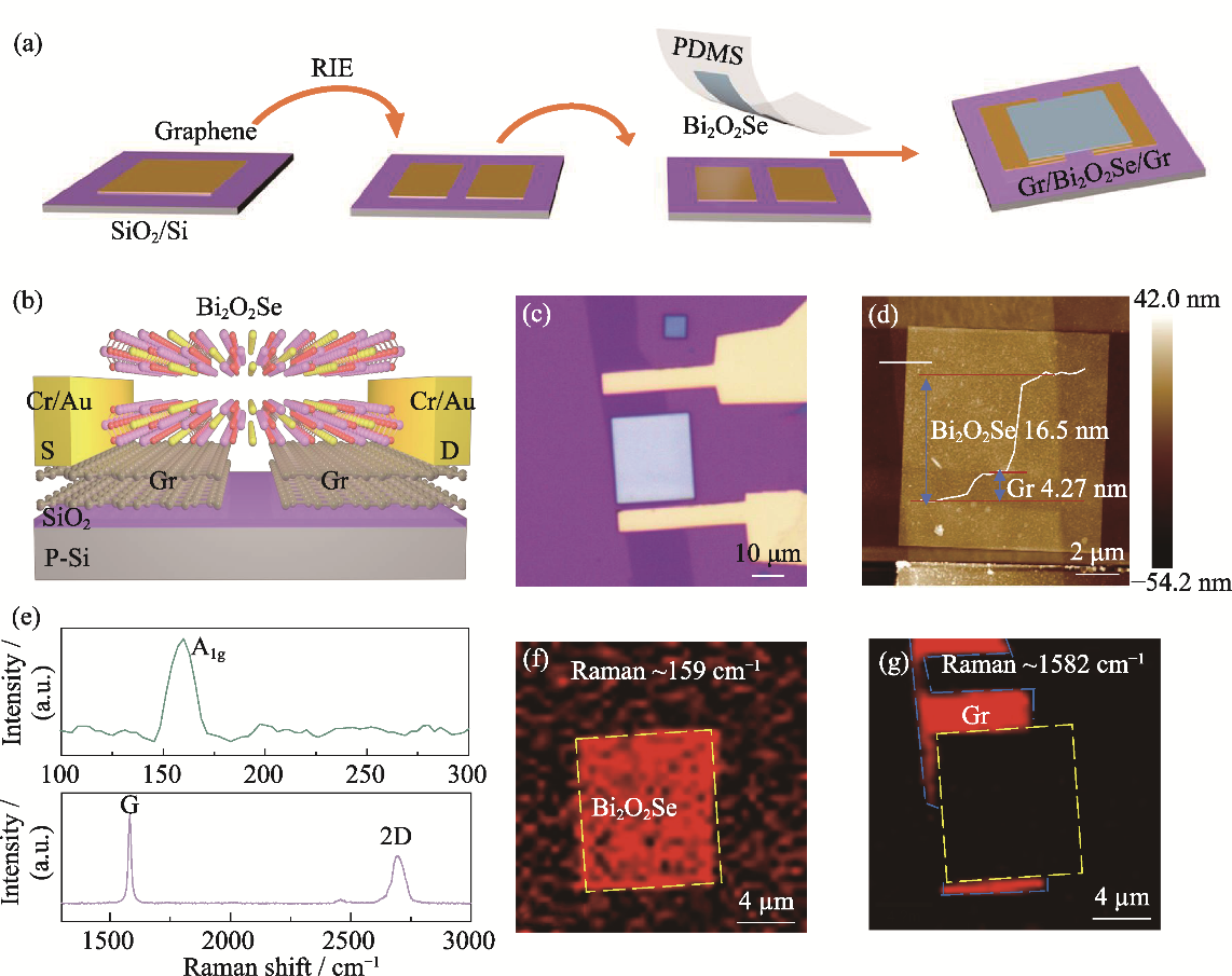
图1 Gr/Bi2O2Se/Gr双异质结器件的结构与表征
Fig. 1 Characterization of Gr/Bi2O2Se/Gr bi-heterostructure device (a) Schematic diagram of device fabrication; (b) Schematic diagram of the structure; (c) Optical microscope image; (d) AFM image and edge height profile; (e) Raman spectra; (f, g) Raman mapping images of (f) Bi2O2Se and (g) graphene
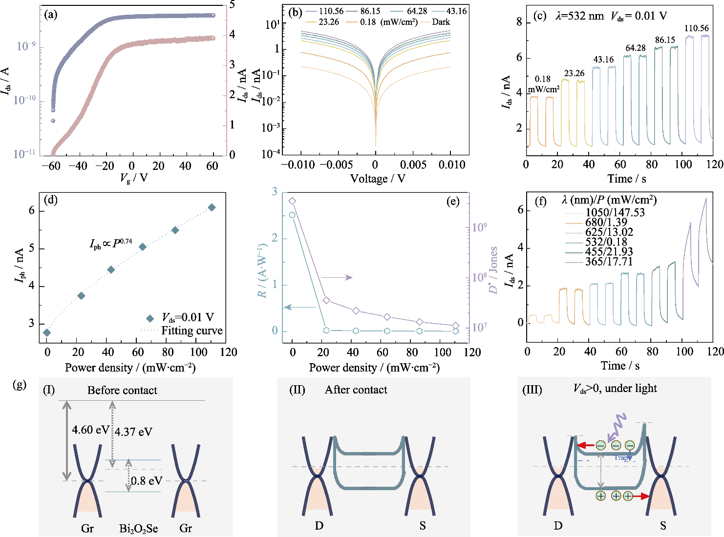
图2 Gr/Bi2O2Se/Gr双异质结器件的性能
Fig. 2 Performance of Gr/Bi2O2Se/Gr bi-heterojunction device (a) Output characteristic curves; (b) Transfer characteristic curves; (c) Photocurrent versus light power density curves; (d) Relationship curve between photocurrent and power density; (e) Responsivity and detectivity; (f) Transient current responses under different illumination wavelengths; (g) Schematic diagrams of the energy bands. Colorful figures are available on website
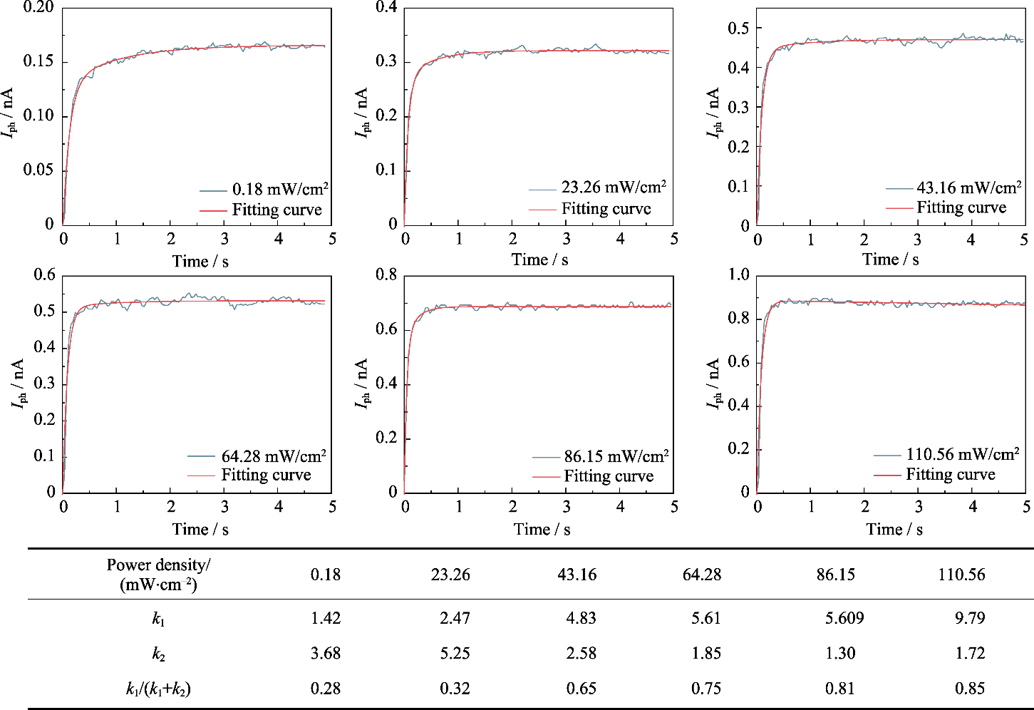
图3 不同光功率密度下的光电流瞬态响应曲线及拟合曲线
Fig. 3 Light current transient response curves and fitting curves under different light power densities Colorful figures are available on website
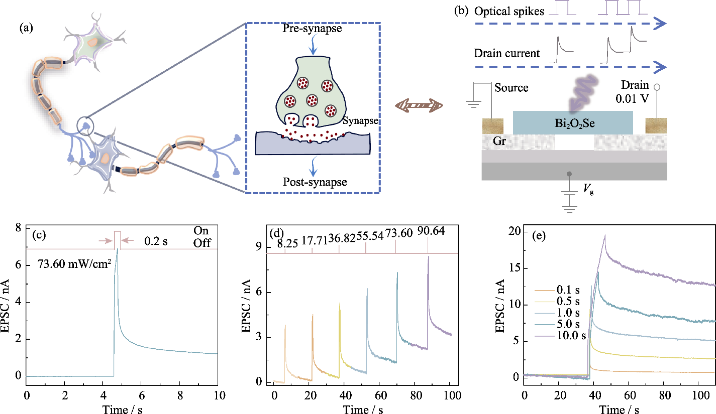
图4 Gr/Bi2O2Se/Gr双异质结器件的光调控突触特性
Fig. 4 Light-regulated synaptic performance of Gr/Bi2O2Se/Gr bi-heterojunction device (a) Schematic diagram of a biological synapse; (b) Schematic diagram of the device working principle; (c) EPSC response of the device under one light pulse; (d) Light intensity dependent EPSC response; (e) EPSC responses under different light pulse durations
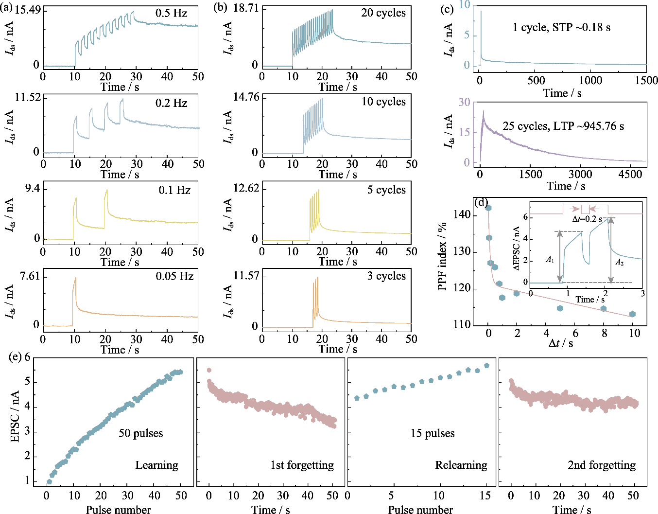
图5 Gr/Bi2O2Se/Gr双异质结器件的突触可塑性
Fig. 5 Synaptic plasticity of Gr/Bi2O2Se/Gr bi-heterojunction device (a) EPSC responses of the device under different light pulse frequencies; (b) Transition from short-term plasticity to long-term plasticity with the increase of light pulse number; (c) Photocurrent decay characteristics; (d) Relationship between paired-pulse facilitation (PPF) index and inter-pulse interval (Δt), with inset showing the excitatory postsynaptic current triggered by a pair of light pulses with a duration of 0.5 s and an interval of 0.2 s; (e) “Learning-forgetting-relearning” behavior of the device
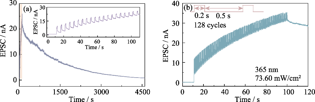
图6 Gr/Bi2O2Se/Gr器件在(a) 25次光脉冲和(b) 128次光脉冲后的保持性能
Fig. 6 Retention behavior of Gr/Bi2O2Se/Gr device after (a) 25 and (b) 128 light pulses
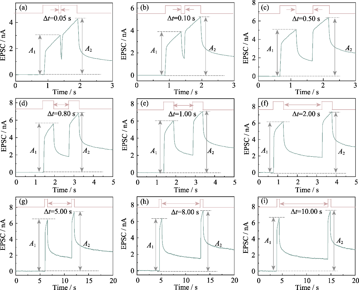
图7 Gr/Bi2O2Se/Gr双异质结器件的PPF行为模拟
Fig. 7 Stimulated PPF behavior of Gr/Bi2O2Se/Gr bi-heterojunction device A pair of light stimuli with a duration of 0.50 s and inter-pulse intervals of (a) 0.05, (b) 0.10, (c) 0.50, (d) 0.80, (e) 1.00, (f) 2.00, (g) 5.00, (h) 8.00 and (i) 10.00 s
| Device | Voltage/V | Wavelength/nm | EPSC/nA | PPF/% | Ref. |
|---|---|---|---|---|---|
| MoS2/h-BN/α-In2Se3 | 1 | 405 | 0.3 | 240 | [ |
| MoS2/SnSe2 | 1 | 400 | 0.3 | 1.25 | [ |
| Bi2O2Se-Vse | 0 | 532 | 0.3 | 133 | [ |
| c-PtTe2/PtSe2 | 1 | 625 | 15 | 1.25 | [ |
| Te/SnS2 | 2 | 532 | 0.1 | 187 | [ |
| p-WSe2/n-Ta2NiS5 | -1 | 1064 | 0.01 | 23 | [ |
| Ph-BTBT-10 2DMC | -1 | 365 | 0.15 | 248 | [ |
| Gr/Bi2O2Se/Gr | 0.01 | 365 | 6.91 | 142.1 | This work |
表1 Gr/Bi2O2Se/Gr器件与已报道光突触的性能参数对比
Table 1 Properties comparison between the Gr/Bi2O2Se/Gr device and other reported synapse
| Device | Voltage/V | Wavelength/nm | EPSC/nA | PPF/% | Ref. |
|---|---|---|---|---|---|
| MoS2/h-BN/α-In2Se3 | 1 | 405 | 0.3 | 240 | [ |
| MoS2/SnSe2 | 1 | 400 | 0.3 | 1.25 | [ |
| Bi2O2Se-Vse | 0 | 532 | 0.3 | 133 | [ |
| c-PtTe2/PtSe2 | 1 | 625 | 15 | 1.25 | [ |
| Te/SnS2 | 2 | 532 | 0.1 | 187 | [ |
| p-WSe2/n-Ta2NiS5 | -1 | 1064 | 0.01 | 23 | [ |
| Ph-BTBT-10 2DMC | -1 | 365 | 0.15 | 248 | [ |
| Gr/Bi2O2Se/Gr | 0.01 | 365 | 6.91 | 142.1 | This work |
| [1] | NOVOSELOV K S, GEIM A K, MOROZOV S V, et al. Electric field effect in atomically thin carbon films. Science, 2004, 306(5696): 666. |
| [2] | KIM K S, KWON J, RYU H, et al. The future of two-dimensional semiconductors beyond Moore’s law. Nature Nanotechnology, 2024, 19(7): 895. |
| [3] | AKINWANDE D, HUYGHEBAERT C, WANG C H, et al. Graphene and two-dimensional materials for silicon technology. Nature, 2019, 573(7775): 507. |
| [4] | XING R, ZHANG X, FAN X, et al. Coupling strategies of multi-physical fields in 2D materials-based photodetectors. Advanced Materials, 2025, 37(16): 2501833. |
| [5] | BA K, WANG J L, HAN M K. Perspectives for infrared properties and applications of MXene. Journal of Inorganic Materials, 2024, 39(2): 162. |
| [6] | WANG S, LIU X, XU M, et al. Two-dimensional devices and integration towards the silicon lines. Nature Materials, 2022, 21(11): 1225. |
| [7] | DAS S, SEBASTIAN A, POP E, et al. Transistors based on two-dimensional materials for future integrated circuits. Nature Electronics, 2021, 4(11): 786. |
| [8] | LIU Y, DUAN X, SHIN H J, et al. Promises and prospects of two-dimensional transistors. Nature, 2021, 591(7848): 43. |
| [9] | TAN C, YU M, TANG J, et al. 2D fin field-effect transistors integrated with epitaxial high-k gate oxide. Nature, 2023, 616(7955): 66. |
| [10] | WYSS K M, LUONG D X, TOUR J M. Large-scale syntheses of 2D materials: flash joule heating and other methods. Advanced Materials, 2022, 34(8): 2106970. |
| [11] | LI L, SHEN G Z. 2D MXenes based flexible photodetectors: progress and prospects. Journal of Inorganic Materials, 2024, 39(2): 186. |
| [12] | LI S, LIU X, YANG H, et al. Two-dimensional perovskite oxide as a photoactive high-κ gate dielectric. Nature Electronics, 2024, 7(3): 216. |
| [13] | ZHANG Q, HOU L, SHAUTSOVA V, et al. Ultrathin all-2D lateral diodes using top and bottom contacted laterally spaced graphene electrodes to WS2 semiconductor monolayers. ACS Applied Materials & Interfaces, 2023, 15(14): 18012. |
| [14] | TAN C, YIN S, CHEN J, et al. Broken-gap PtS2/WSe2 van der Waals heterojunction with ultrahigh reverse rectification and fast photoresponse. ACS Nano, 2021, 15(5): 8328. |
| [15] | WU F, XIA H, SUN H, et al. AsP/InSe van der Waals tunneling heterojunctions with ultrahigh reverse rectification ratio and high photosensitivity. Advanced Functional Materials, 2019, 29(12): 1900314. |
| [16] | LIU X, QU D, LI H M, et al. Modulation of quantum tunneling via a vertical two-dimensional black phosphorus and molybdenum disulfide p-n junction. ACS Nano, 2017, 11(9): 9143. |
| [17] | LI J, WANG Z, WEN Y, et al. High-performance near-infrared photodetector based on ultrathin Bi2O2Se nanosheets. Advanced Functional Materials, 2018, 28(10): 1706437. |
| [18] | WANG W, MENG Y, ZHANG Y, et al. High electron mobility and quantum oscillations in non-encapsulated ultrathin semiconducting Bi2O2Se. Nature Nanotechnology, 2017, 12: 530. |
| [19] | YIN J, TAN Z, HONG H, et al. Ultrafast and highly sensitive infrared photodetectors based on two-dimensional oxyselenide crystals. Nature Communications, 2018, 9: 3311. |
| [20] | ZHANG Z, LI T, WU Y, et al. Truly concomitant and independently expressed short-and long-term plasticity in a Bi2O2Se-based three-terminal memristor. Advanced Materials, 2019, 31(3): 1805769. |
| [21] | LUO P, ZHUGE F, WANG F, et al. PbSe quantum dots sensitized high-mobility Bi2O2Se nanosheets for high-performance and broadband photodetection beyond 2 μm. ACS Nano, 2019, 13(8): 9028. |
| [22] | FAKIH I, DURNAN O, MAHVASH F, et al. Selective ion sensing with high resolution large area graphene field effect transistor arrays. Nature Communications, 2020, 11: 3226. |
| [23] | WANG W, MENG Y, WANG W, et al. Highly efficient full van der Waals 1D p-Te/2D n-Bi2O2Se heterodiodes with nanoscale ultra-photosensitive channels. Advanced Functional Materials, 2022, 32(30): 2203003. |
| [24] | LIU W, LV J, PENG L, et al. Graphene charge-injection photodetectors. Nature Electronics, 2022, 5(5): 281. |
| [25] | SHIN J, YOO H. Photogating effect-driven photodetectors and their emerging applications. Nanomaterials, 2023, 13(5): 882. |
| [26] | TSAI T H, LIANG Z Y, LIN Y C, et al. Photogating WS2 photodetectors using embedded WSe2 charge puddles. ACS nano, 2020, 14(4): 4559. |
| [27] | 张世斌, 孔光临, 徐艳月, 等. 微量硼掺杂非晶硅的瞬态光电导衰退及其光致变化. 物理学报, 2002, 51(1): 111. |
| [28] | HAN J, FANG C, YU M, et al. A high-performance Schottky photodiode with asymmetric metal contacts constructed on 2D Bi2O2Se. Advanced Electronic Materials, 2022, 8(7): 2100987. |
| [29] | LIU J, HAO Q, GAN H, et al. Selectively modulated photoresponse in type-I heterojunction for ultrasensitive self-powered photodetectors. Laser & Photonics Reviews, 2022, 16(11): 2200338. |
| [30] | YANG J L, WANG L J, RUAN S Y, et al. Highly weak-light sensitive and dual-band switchable photodetector based on CuI/Si unilateral heterojunction. Journal of Inorganic Materials, 2024, 39(9): 1063. |
| [31] | LIU C H, CHANG Y C, NORRIS T B, et al. Graphene photodetectors with ultra-broadband and high responsivity at room temperature. Nature nanotechnology, 2014, 9(4): 273. |
| [32] | SUN L, XU Y, HUO G, et al. Multifunctional neuromorphic optoelectronic computing using all 2D floating-gate transistors. Nano Energy, 2025, 143: 111311. |
| [33] | GAO W, ZHANG S, ZHANG F, et al. 2D WS2 based asymmetric Schottky photodetector with high performance. Advanced Electronic Materials, 2021, 7(7): 2000964. |
| [34] | CHEN J, ZHANG Z, FENG J, et al. 2D InSe self-powered Schottky photodetector with the same metal in asymmetric contacts. Advanced Materials Interfaces, 2022, 9(35): 2200075. |
| [35] | HUANG W, HANG P, WANG Y, et al. Zero-power optoelectronic synaptic devices. Nano Energy, 2020, 73: 104790. |
| [36] | HAO Z, WANG H, JIANG S, et al. Retina-inspired self-powered artificial optoelectronic synapses with selective detection in organic asymmetric heterojunctions. Advanced Science, 2022, 9(7): 2103494. |
| [37] | WANG J Y, WAN C J, WAN Q. Dual-gate IGZO-based neuromorphic transistors with stacked Al2O3/chitosan gate dielectrics. Journal of Inorganic Materials, 2023, 38(4): 445. |
| [38] | WANG X, ZONG Y, LIU D, et al. Advanced optoelectronic devices for neuromorphic analog based on low-dimensional semiconductors. Advanced Functional Materials, 2023, 33(15): 2213894. |
| [39] | ZHANG H S, DONG X M, ZHANG Z C, et al. Co-assembled perylene/graphene oxide photosensitive heterobilayer for efficient neuromorphics. Nature Communications, 2022, 13: 4996. |
| [40] | WANG W X, GAO S, LI Y, et al. Artificial optoelectronic synapses based on TiNxO2-x/MoS2 heterojunction for neuromorphic computing and visual system. Advanced Functional Materials, 2021, 31(34): 2101201. |
| [41] | HUANG W, HANG P, XIA X, et al. Two-terminal self-rectifying optoelectronic synaptic devices with largest-dynamic-range updates. Applied Materials Today, 2023, 30: 101728. |
| [42] | HE J, CHEN K, HUANG C, et al. Explicit gain equations for single crystalline photoconductors. ACS Nano, 2020, 14(3): 3405. |
| [43] | LI X, CHEN F, WANG X, et al. Emulation of optical and electrical synaptic functions in MoS2/SnSe2 van der Waals heterojunction memtransistors. Japanese Journal of Applied Physics, 2024, 63(5): 056502. |
| [44] | REN X, HE X, DUAN Z, et al. Self-powered and broadband optical synapse device based on Se-vacancy Bi2O2Se for artificial vision system application. ACS Photonics, 2024, 11(11): 4990. |
| [45] | HAN S S, SHIN J C, GHANIPOUR A, et al. High mobility transistors and flexible optical synapses enabled by wafer-scale chemical transformation of Pt-based 2D layers. ACS Applied Materials & Interfaces, 2024, 16(28): 36599. |
| [46] | ZHANG Y, TANG Y, LIU K, et al. Optoelectronic synapse based on Te/SnS2 heterostructure with integrated sensing-memory- computing for neuromorphic visual system. Advanced Optical Materials, 2025, 13(26): e01371. |
| [47] | HOU P, TAN S, ZHENG S. Design and implementation of an infrared artificial visual neural synapse based on a p-WSe2/ n-Ta2NiS5 van der Waals heterojunction. Journal of Materials Chemistry C, 2024, 12(41): 16722. |
| [48] | DONG M, ZHANG Y, ZHU J, et al. All-in-one 2D molecular crystal optoelectronic synapse for polarization-sensitive neuromorphic visual system. Advanced Materials, 2024, 36(40): 2409550. |
| [1] | 汪加辉, 刘晶晶, 邱毅, 王永霞, 崔香枝. 原子级铁锚定氮掺杂石墨烯的双功能氧电催化性能[J]. 无机材料学报, 2026, 41(6): 814-822. |
| [2] | 秦英, 姚焯, 郑丽君, 包硕, 李鹏, 郭诗淇. 柔性超级电容器硫掺杂石墨烯/导电聚合物复合电极材料的制备及性能研究[J]. 无机材料学报, 2026, 41(5): 604-610. |
| [3] | 程澳芃, 王跃文, 许文涛, 刘全伟, 张海涛, 周有福. 吸附-沉淀自组装结合放电等离子烧结法制备石墨烯增强氧化铝复合陶瓷[J]. 无机材料学报, 2026, 41(4): 536-544. |
| [4] | 朱开煌, 杨世杰, 李欣格, 宋贯卿, 史淦升, 王焱, 任小孟, 陆遥, 徐新宏, 孙静. 基于UiO-66骨架的氧化石墨烯改性金属有机框架凝胶的制备及其对甲苯的高效吸附性能[J]. 无机材料学报, 2026, 41(4): 519-526. |
| [5] | 范雨竹, 王媛, 王林燕, 向美玲, 鄢雨婷, 黎本慧, 李敏, 文志东, 王海超, 陈永福, 邱会东, 赵波, 周成裕. 氧化石墨烯基吸附材料去除水体中Pb(II): 制备、性能及机理[J]. 无机材料学报, 2026, 41(1): 12-26. |
| [6] | 杨茗凯, 黄泽皑, 周芸霄, 刘彤, 张魁魁, 谭浩, 刘梦颖, 詹俊杰, 陈国星, 周莹. 基于Cu与金属氧化物-KCl熔融介质的甲烷热解制备少层石墨烯与氢气联产研究[J]. 无机材料学报, 2025, 40(5): 473-480. |
| [7] | 高晨光, 孙晓亮, 陈君, 李达鑫, 陈庆庆, 贾德昌, 周玉. 基于湿法纺丝技术的SiBCN-rGO陶瓷纤维的组织结构、力学和吸波性能[J]. 无机材料学报, 2025, 40(3): 290-296. |
| [8] | 王悦, 王欣, 于显利. 室温铁磁性还原氧化石墨烯基全碳膜[J]. 无机材料学报, 2025, 40(3): 305-313. |
| [9] | 李红兰, 张俊苗, 宋二红, 杨兴林. Mo/S共掺杂的石墨烯用于合成氨: 密度泛函理论研究[J]. 无机材料学报, 2024, 39(5): 561-568. |
| [10] | 孙川, 何鹏飞, 胡振峰, 王荣, 邢悦, 张志彬, 李竞龙, 万春磊, 梁秀兵. 含有石墨烯阵列的SiC基陶瓷材料的制备与力学性能[J]. 无机材料学报, 2024, 39(3): 267-273. |
| [11] | 万胡杰, 肖旭. MXenes及其复合物的太赫兹电磁屏蔽与吸收[J]. 无机材料学报, 2024, 39(2): 129-144. |
| [12] | 王艳莉, 钱心怡, 沈春银, 詹亮. 石墨烯基介孔锰铈氧化物催化剂: 制备和低温催化还原NO[J]. 无机材料学报, 2024, 39(1): 81-89. |
| [13] | 杨平军, 李铁虎, 李昊, 党阿磊. 石墨烯对环氧树脂泡沫炭石墨化、电导率和力学性能的影响[J]. 无机材料学报, 2024, 39(1): 107-112. |
| [14] | 董怡曼, 谭占鳌. 宽带隙钙钛矿基二端叠层太阳电池复合层的研究进展[J]. 无机材料学报, 2023, 38(9): 1031-1043. |
| [15] | 李涛, 曹鹏飞, 胡力涛, 夏勇, 陈一, 刘跃军, 孙翱魁. NH4+扩层MoS2的制备及其储锌性能研究[J]. 无机材料学报, 2023, 38(1): 79-86. |
| 阅读次数 | ||||||
|
全文 |
|
|||||
|
摘要 |
|
|||||