Journal of Inorganic Materials ›› 2021, Vol. 36 ›› Issue (6): 570-578.DOI: 10.15541/jim20200361
Special Issue: 能源材料论文精选(2021); 【虚拟专辑】太阳能电池(2020~2021)
• REVIEW • Previous Articles Next Articles
WU Xiaowei1,2( ), LI Jiayan1,2()
Received:2020-06-30
Revised:2020-08-30
Published:2021-06-20
Online:2020-10-10
Contact:
LI Jiayan, associate professor. E-mail: lijiayan@dlut.edu.cn
About author:WU Xiaowei(1991-), male, PhD candidate. E-mail: wuxiaowei261@163.com
Supported by:CLC Number:
WU Xiaowei, LI Jiayan. Texturing Technology on Multicrystalline Silicon Wafer by Metal-catalyzed Chemical Etching: a Review[J]. Journal of Inorganic Materials, 2021, 36(6): 570-578.
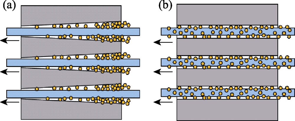
Fig. 1 Schematic diagram of (a) MWSS cut technique and (b) DWS cut technique

Fig. 2 SEM images of (a, b) MWSS cut and (c, d) DWS cut multicrystalline silicon wafer surface
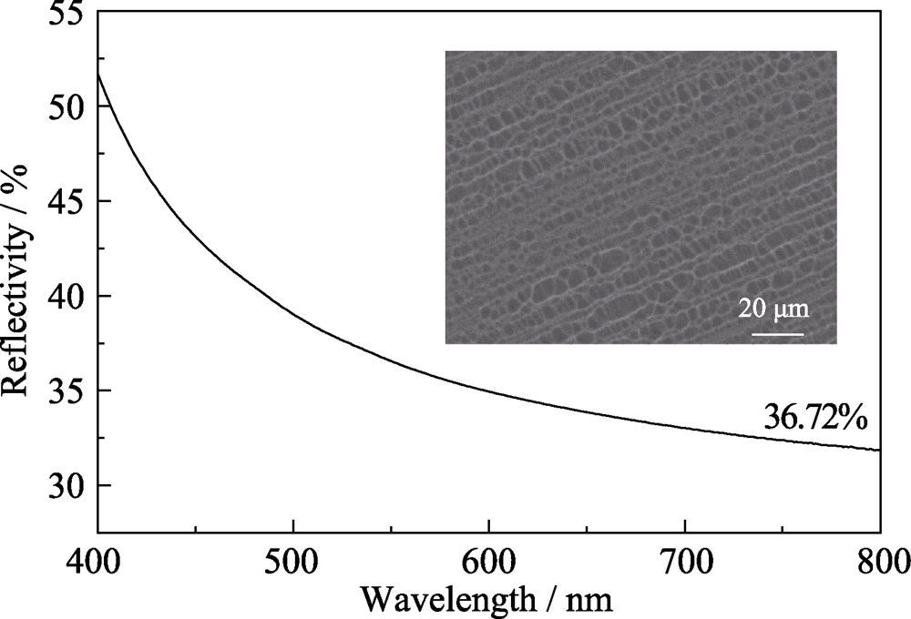
Fig. 3 Surface SEM morphology and reflectivity for texture surface of silicon wafer by acid etching

Fig. 4 Schematic diagram of MCCE[18]

Fig. 5 SEM images of silicon surfaces with (a) nano-texture, (b) micro-texture and (c) nano-micro-texture[31]
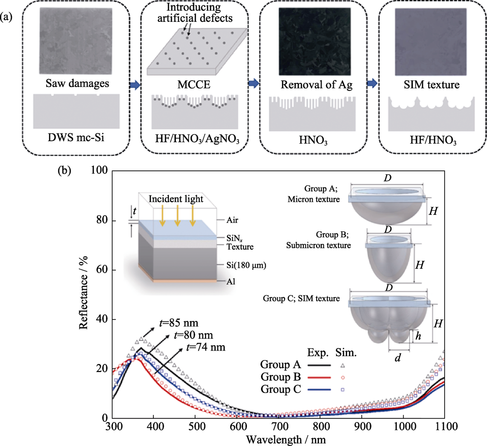
Fig. 6 (a) Schematic illustration of the main steps to prepare the submicron-in-micron (SIM) texture on the DWS mc-Si wafer and (b) experimental reflectance (curves) and simulated reflectance (scatter points) of three samples[33]
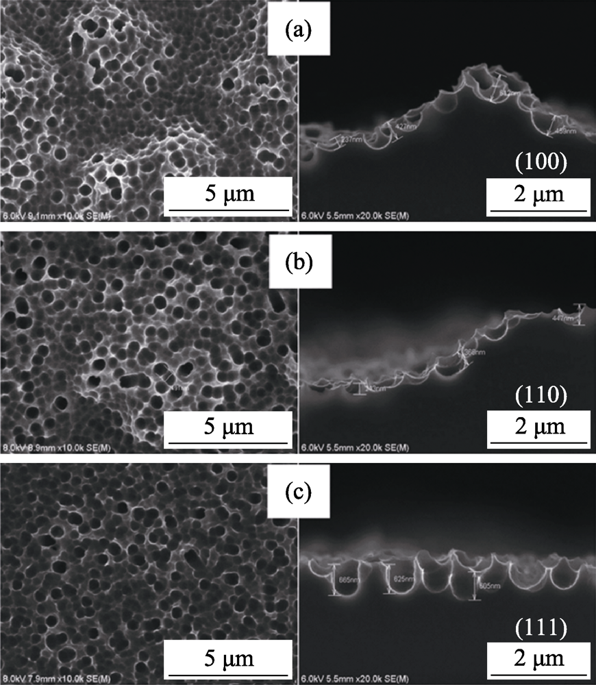
Fig. 7 Surface and cross-sectional SEM images of mc-Si grains after etching by alkali, Ag-MCCE and post-etching with different orientations[34] (a) (100); (b) (110); (c) (111)
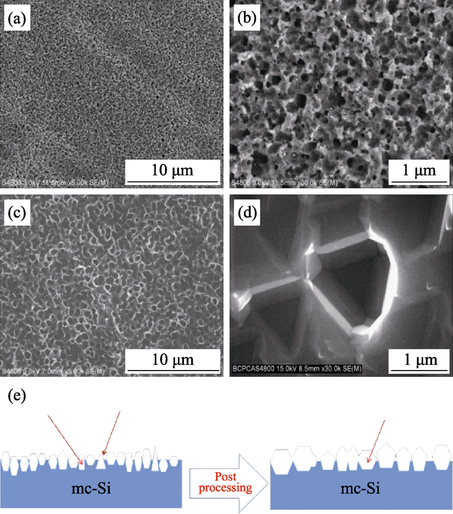
Fig. 8 SEM images of Si nanostructures produced by Cu-MCCE method (a,b) before and (c,d) after the post-processing treatment and (e) schematic diagram of post-processing treatment[41]

Fig. 9 Cross-sectional SEM images of Si wafers after (a) Ag-MCCE and (b) Cu-MCCE, and (c) schematics of etching process by single Cu- and Ag-catalyzed chemical etching and Ag/Cu-cocatalyzed chemical etching[45]
| Catalyst | Method | Ra | ηb | Ref. |
|---|---|---|---|---|
| Ag | Ag-MCCE + HF/HNO3+NaOH | 15.9% | 18.45% | [ |
| Ag | Artificial defects (HF/HNO3/AgNO3)+HF/HNO3 | 19% | 19.07% | [ |
| Ag | Alkali etching+Ag-MCCE+post etching | 16.85% | 19.4% | [ |
| Ag | Ag deposition (additive)+etching | 16.04% | 19.51% | [ |
| Ag | Ag deposition+etching (additive) | 18.17% | 19.56% | [ |
| Ag | HF/HNO3+Ag-MCCE+RIE | - | 20.69% | [ |
| Ag | Ag-MCCE | 23.7% | 20.89% | [ |
| Ag | Ag-MCCE+Modification by acid etching | 19.46% | 19.07% | [ |
| Ag | HF/HNO3+Ag-MCCE+NSR process | 8.26% | 17.96% | [ |
| Ag | HF/HNO3+Ag-MCCE+HF/HNO3 | 18.4% | 18.7% | [ |
| Cu | Cu-MCCE+post etching (HF/HNO3/H3PO4) | - | 18.88% | [ |
| Cu | Cu-MCCE+HF/HNO3 | 18.21% | 19.06% | [ |
| Cu | Cu-MCCE | 22.4% | 19.03% | [ |
| Ag-Cu | Cu/Ag-MCCE | 12.08% | 19.49% | [ |
| Ag-Cu | Alkali pretreatment (additive)+Cu/Ag-MCCE+post etching | 15.52% | 18.91% | [ |
| Ag-Cu | Cu/Ag-MCCE + NSR (H2O2/NaF) | 16.50% | 18.71% | [ |
| Ag-Cu | Cu/Ag-MCCE + NSR (H2O2/NaF) | 16.85% | 19.10% | [ |
| Ni | Ni-MCCE | - | 16.60% | [ |
| Cu-Ni | Cu/Ni-MCCE (Cu(NO3)2+NiSO4+HF+H2O2) | 18.53% | - | [ |
Table 1 Performances for texture surfaces of DWS cut multicrystalline silicon prepared via different MCCE methods
| Catalyst | Method | Ra | ηb | Ref. |
|---|---|---|---|---|
| Ag | Ag-MCCE + HF/HNO3+NaOH | 15.9% | 18.45% | [ |
| Ag | Artificial defects (HF/HNO3/AgNO3)+HF/HNO3 | 19% | 19.07% | [ |
| Ag | Alkali etching+Ag-MCCE+post etching | 16.85% | 19.4% | [ |
| Ag | Ag deposition (additive)+etching | 16.04% | 19.51% | [ |
| Ag | Ag deposition+etching (additive) | 18.17% | 19.56% | [ |
| Ag | HF/HNO3+Ag-MCCE+RIE | - | 20.69% | [ |
| Ag | Ag-MCCE | 23.7% | 20.89% | [ |
| Ag | Ag-MCCE+Modification by acid etching | 19.46% | 19.07% | [ |
| Ag | HF/HNO3+Ag-MCCE+NSR process | 8.26% | 17.96% | [ |
| Ag | HF/HNO3+Ag-MCCE+HF/HNO3 | 18.4% | 18.7% | [ |
| Cu | Cu-MCCE+post etching (HF/HNO3/H3PO4) | - | 18.88% | [ |
| Cu | Cu-MCCE+HF/HNO3 | 18.21% | 19.06% | [ |
| Cu | Cu-MCCE | 22.4% | 19.03% | [ |
| Ag-Cu | Cu/Ag-MCCE | 12.08% | 19.49% | [ |
| Ag-Cu | Alkali pretreatment (additive)+Cu/Ag-MCCE+post etching | 15.52% | 18.91% | [ |
| Ag-Cu | Cu/Ag-MCCE + NSR (H2O2/NaF) | 16.50% | 18.71% | [ |
| Ag-Cu | Cu/Ag-MCCE + NSR (H2O2/NaF) | 16.85% | 19.10% | [ |
| Ni | Ni-MCCE | - | 16.60% | [ |
| Cu-Ni | Cu/Ni-MCCE (Cu(NO3)2+NiSO4+HF+H2O2) | 18.53% | - | [ |
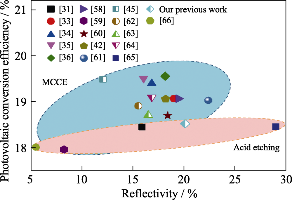
Fig. 10 Relation between η of solar cells and reflectivity of texture surface[31,33-36,42,45,58-65]
| Method | Advantages | Disadvantages | η |
|---|---|---|---|
| Ag-MCCE | Mature technology, easy to form nanostructure, stable performance | High cost, difficult to recycle waste liquid | 20.89% |
| Cu-MCCE | Low cost, easy to remove residual Cu, significantly reduce the impact of saw marks | Easy to form the dense film, decreased etching rate, essential oxidants | 19.06% |
| MCCE-additive | Uniform size, stable performance | Organic compounds increasing the cost of waste liquid treatment | 19.56% |
| Composite MCCE | Composite structure | Complicated process, and difficult to recycle the waste liquid | 19.49% |
| Other metal-MCCE | Low cost, composite structure | Inmature | 16.60% |
Table 2 Comparison of making texture surface on DWS cut multicrystalline silicon by different MCCE methods
| Method | Advantages | Disadvantages | η |
|---|---|---|---|
| Ag-MCCE | Mature technology, easy to form nanostructure, stable performance | High cost, difficult to recycle waste liquid | 20.89% |
| Cu-MCCE | Low cost, easy to remove residual Cu, significantly reduce the impact of saw marks | Easy to form the dense film, decreased etching rate, essential oxidants | 19.06% |
| MCCE-additive | Uniform size, stable performance | Organic compounds increasing the cost of waste liquid treatment | 19.56% |
| Composite MCCE | Composite structure | Complicated process, and difficult to recycle the waste liquid | 19.49% |
| Other metal-MCCE | Low cost, composite structure | Inmature | 16.60% |
| [1] |
ADEBISI J A, AGUNSOYE J O, BELLO S A, et al. Potential of producing solar grade silicon nanoparticles from selected agro-wastes: a review. Sol. Energy, 2017,142:68-86.
DOI URL |
| [2] |
YIN Y, GAO Y, LI X, et al. Experimental study on slicing photovoltaic polycrystalline silicon with diamond wire saw. Mat. Sci. Semicon. Proc., 2020,106:104779.
DOI URL |
| [3] |
BASHER M K, MISHAN R, BISWAS S, et al. Study and analysis the Cu nanoparticle assisted texturization forming low reflective silicon surface for solar cell application. AIP Adv., 2019,9:075118.
DOI URL |
| [4] | ANDREANI L C, BOZZOLA A, KOWALCZEWSKI P, et al. Silicon solar cells: toward the efficiency limits. Adv. Phys. X, 2019,4(1):1548305. |
| [5] |
HUANG B J, ZHAO J, CHAI J Y, et al. Environmental influence assessment of China's multi-crystalline silicon (multi-Si) photovoltaic modules considering recycling process. Sol. Energy, 2017,143:132-141.
DOI URL |
| [6] |
MÖLLER H J, FUNKE C, RINIO M, et al. Multicrystalline silicon for solar cells. Thin Solid Films, 2005,487(1):179-187.
DOI URL |
| [7] |
MEINEL B, KOSCHWITZ T, BLOCKS C, et al. Comparison of diamond wire cut and silicon carbide slurry processed silicon wafer surfaces after acidic texturisation. Mat. Sci. Semicon. Proc., 2014,26:93-100.
DOI URL |
| [8] |
WU Y F, CHEN Y M. Separation of silicon and silicon carbide using an electrical field. Sep. Purif. Technol., 2009,68(1):70-74.
DOI URL |
| [9] |
HARDIN C W, QU J, SHIH A J. Fixed abrasive diamond wire saw slicing of single-crystal silicon carbide wafers. Mater. Manuf. Processes, 2004,19(2):355-367.
DOI URL |
| [10] | QIU M B, HUANG Y H, LIU Z D, et al. A review of the fabrication methods for solar silicon wafer. Mechanical Science and Technology for Aerospace Engineering, 2008,27(8):1017-1020. |
| [11] | CAI E, TANG B, FAHRNER W R, et al. Characterization of the Surfaces Generated by Diamond Cutting of Crystalline Silicon. 26th European Photovoltaic Solar Energy Conference and Exhibition. Hamburg, 2011: 1884-1886. |
| [12] | CHEN C C A, CHAO P H. Surface texture analysis of fixed and free abrasive machining of silicon substrates for solar cell. Adv. Mater. Res., 2010, 126-128:177-180. |
| [13] | BIDIVILLE A, WASMER K, KRAFT R, et al. Diamond Wire-sawn Silicon Wafers-from the Lab to the Cell Production. 24th European Photovoltaic Solar Energy Conference and Exhibition. Hamburg, 2009: 1400-1405. |
| [14] |
LIPPOLD M, BUCHHOLZ F, GONDEK C, et al. Texturing of SiC-slurry and diamond wire sawn silicon wafers by HF-HNO3-H2SO4 mixtures. Sol. Energ. Mat. Sol. C, 2014,127:104-110.
DOI URL |
| [15] |
MEMMING R, SCHWANDT G. Anodic dissolution of silicon in hydrofluoric acid solutions. Surf. Sci., 1966,4(2):109-124
DOI URL |
| [16] |
XIAO Z G, GENG G Y, WEI X Q, et al. On the mechanism of the vapor etching of diamond wire sawn multi-crystalline silicon wafers for texturing. Mat. Sci. Semicon. Proc., 2016,53:8-12.
DOI URL |
| [17] |
JANSEN H, DEBOER M, LEGTENBERG R, et al. The black silicon method-a universal method for determining the parameter setting of a fluorine-based reactive ion etcher in deep silicon trench etching with profile control. J. Micromech. Microeng., 1995,5(2):115-120.
DOI URL |
| [18] |
HUANG Z P, GEYER N, WERNER P, et al. Metal-assisted chemical etching of silicon: a review. Adv. Mater., 2011,23(2):285-308.
DOI URL |
| [19] |
HSU C, WU J R, LU Y T, et al. Fabrication and characteristics of black silicon for solar cell applications: an overview. Mat. Sci. Semicon. Proc., 2014,25:2-17.
DOI URL |
| [20] |
DIMOVA-MALINOVSKA D, SENDOVA-VASSILEVA M, TZENOV N, et al. Preparation of thin porous silicon layers by stain etching. Thin Solid Films, 1997,297(1/2):9-12.
DOI URL |
| [21] |
LI X, BOHN P W. Metal-assisted chemical etching in HF/H2O2 produces porous silicon. Appl. Phys. Lett., 2000,77(16):2572-2574.
DOI URL |
| [22] |
HUANG Z P, WU Y, FANG H, et al. Large-scale Si1-xGex quantum dot arrays fabricated by templated catalytic etching. Nanotechnology, 2006,17(5):1476-1480.
DOI URL |
| [23] |
HUANG Z, SHIMIZU T, SENZ S, et al. Ordered arrays of vertically aligned [110] silicon nanowires by suppressing the crystallographically preferred <100> etching directions. Nano Lett., 2009,9(7):2519-2525.
DOI URL |
| [24] |
PENG K Q, HU J J, YAN Y J, et al. Fabrication of single-crystalline silicon nanowires by scratching a silicon surface with catalytic metal particles. Adv. Funct. Mater., 2006,16(3):387-394.
DOI URL |
| [25] |
CHATTOPADHYAY S, BOHN P W. Direct-write patterning of microstructured porous silicon arrays by focused-ion-beam Pt deposition and metal-assisted electroless etching. J. Appl. Phys., 2004,96(11):6888-6894.
DOI URL |
| [26] |
NIU Y C, LIU H T, LIU X J, et al. Study on nano-pores enlargement during Ag-assisted electroless etching of diamond wire sawn polycrystalline silicon wafers. Mat. Sci. Semicon. Proc., 2016,56:119-126.
DOI URL |
| [27] |
SU G Y, DAI X W, SUN H C, et al. The study of the defect removal etching of black silicon for diamond wire sawn multi-crystalline silicon solar cells. Sol. Energy, 2018,170:95-101.
DOI URL |
| [28] |
CAO F, CHEN K X, ZHANG J J, et al. Next-generation multi-crystalline silicon solar cells: diamond-wire sawing, nano-texture and high efficiency. Sol. Energ. Mat. Sol. C, 2015,141:132-138.
DOI URL |
| [29] |
KUMAGAI A. Texturization using metal catalyst wet chemical etching for multicrystalline diamond wire sawn wafer. Sol. Energ. Mat. Sol. C, 2015,133:216-222.
DOI URL |
| [30] | PENG K, FANG H, HU J, et al. Metal-particle-induced, highly localized site-specific etching of Si and formation of single-crystalline Si nanowires in aqueous fluoride solution. Chemistry, 2006,12(30):7942-7947. |
| [31] |
ZHUANG Y F, ZHONG S H, HUANG Z G, et al. Versatile strategies for improving the performance of diamond wire sawn mc-Si solar cells. Sol. Energ. Mat. Sol. C, 2016,153:18-24.
DOI URL |
| [32] |
ZHANG P F, JIA R, TAO K, et al. The influence of Ag-ion concentration on the performance of mc-Si silicon solar cells textured by metal assisted chemical etching (MACE) method. Sol. Energ. Mat. Sol. C, 2019,200:109983.
DOI URL |
| [33] |
WU C K, ZOU S, ZHU J Y, et al. Forming submicron in micron texture on the diamond-wire-sawn mc-Si wafer by introducing artificial defects. Prog. Photovoltaics, 2020,28:788-797.
DOI URL |
| [34] |
ZOU S, YE X Y, WU C K, et al. Complementary etching behavior of alkali, metal-catalyzed chemical, and post-etching of multicrystalline silicon wafers. Prog. Photovoltaics, 2019,27(6):511-519.
DOI URL |
| [35] |
LI X P, TAO K, ZHANG D, et al. Development of additive-assisted Ag-MACE for multicrystalline black Si solar cells. Electrochem. Commun., 2020,113:106686.
DOI URL |
| [36] |
LI X P, GAO Z B, ZHANG D, et al. High-efficiency multi-crystalline black silicon solar cells achieved by additive assisted Ag-MACE. Sol. Energy, 2020,195:176-184.
DOI URL |
| [37] |
PENG K Q, ZHU J. Morphological selection of electroless metal deposits on silicon in aqueous fluoride solution. Electrochim Acta, 2004,49(16):2563-2568.
DOI URL |
| [38] |
CAO M, LI S Y, DENG J X, et al. Texturing a pyramid-like structure on a silicon surface via the synergetic effect of copper and Fe(III) in hydrofluoric acid solution. Appl Surf. Sci., 2016,372:36-41.
DOI URL |
| [39] | ZOU Y X, XI F S, QIU J J, et al. Cu-assisted chemical etching of diamond wire sawn multicrystalline silicon wafers for texturing. China Surface Engineering, 2017,30(6):59-66. |
| [40] |
SHENG G Z, ZOU Y X, LI S Y, et al. Controllable nano-texturing of diamond wire sawing polysilicon wafers through low-cost copper catalyzed chemical etching. Mater. Lett., 2018,221:85-88.
DOI URL |
| [41] |
WANG P, XIAO S Q, JIA R, et al. 18.88%-efficient multi-crystalline silicon solar cells by combining Cu-catalyzed chemical etching and post-treatment process. Sol Energy, 2018,169:153-158.
DOI URL |
| [42] |
ZHA J W, WANG T, PAN C F, et al. Constructing submicron textures on mc-Si solar cells via copper-catalyzed chemical etching. Appl. Phys. Lett., 2017,110(9):093901.
DOI URL |
| [43] | ZHENG C F, SHEN H L, PU T, et al. Fabrication and property of anti-reflection structures on multicrystalline silicon by Ag and Cu dually assisted chemical etching. J. Funct. Mater., 2017,48(1):1230-1235. |
| [44] |
WANG S D, CHEN T W. Texturization of diamond-wire-sawn multicrystalline silicon wafer using Cu, Ag, or Ag/Cu as a metal catalyst. Appl. Surf. Sci., 2018,444:530-541.
DOI URL |
| [45] |
CHEN W, LIU Y P, WU J T, et al. High-efficient solar cells textured by Cu/Ag-cocatalyzed chemical etching on diamond wire sawing multicrystalline silicon. ACS Appl. Mater. Inter., 2019,11(10):10052-10058.
DOI URL |
| [46] |
YUE Z H, SHEN H L, JIANG Y, et al. Novel and low reflective silicon surface fabricated by Ni-assisted electroless etching and coated with atomic layer deposited Al2O3 film. Appl. Phys. A-Mater., 2013,114(3):813-817.
DOI URL |
| [47] |
TAKALOO A V, ES F, BAYTEMIR G, et al. Nickel assisted chemical etching for multi-crystalline Si solar cell texturing: a low cost single step alternative to existing methods. Mater. Res. Express, 2018,5(7):075506.
DOI URL |
| [48] |
GAO K, SHEN H L, LIU Y W, et al. Enhanced etching rate of black silicon by Cu/Ni Co-assisted chemical etching process. Mat. Sci. Semicon. Proc., 2018,88:250-255.
DOI URL |
| [49] |
LAI R A, HYMEL T M, NARASIMHAN V K, et al. Schottky barrier catalysis mechanism in metal-assisted chemical etching of silicon. ACS Appl. Mater. Inter., 2016,8(14):8875-8879.
DOI URL |
| [50] |
MAURYA M R, TOUTAM V, SINGH P, et al. Optimization of electroless plating of gold during MACE for through etching of silicon wafer. Mat. Sci. Semicon. Proc., 2019,100:140-144.
DOI URL |
| [51] |
XIE T, SCHMIDT V, PIPPEL E, et al. Gold-enhanced low-temperature oxidation of silicon nanowires. Small, 2008,4(1):64-68.
DOI URL |
| [52] |
BAYTEMIR G, CIFTPINAR E H, TURAN R. Enhanced metal assisted etching method for high aspect ratio microstructures: applications in silicon micropillar array solar cells. Sol. Energy, 2019,194:148-155.
DOI URL |
| [53] |
YAE S, KAWAMOTO Y, TANAKA H, et al. Formation of porous silicon by metal particle enhanced chemical etching in HF solution and its application for efficient solar cells. Electrochem. Commun., 2003,5(8):632-636.
DOI URL |
| [54] |
CHATTOPADHYAY S, LI X, BOHN P W. In-plane control of morphology and tunable photoluminescence in porous silicon produced by metal-assisted electroless chemical etching. J. Appl. Phys., 2002,91(9):6134-6140.
DOI URL |
| [55] |
ZHU B, LIU W J, DING S J, et al. Formation mechanism of heavily doped silicon mesopores induced by Pt nanoparticle-assisted chemical etching. J. Phys. Chem. C, 2018,122(37):21537-21542.
DOI URL |
| [56] |
JIN J, SHEN H, ZHENG P, et al. >20.5% diamond wire sawn multicrystalline silicon solar cells with maskless inverted pyramid like texturing. IEEE J. Photovolt., 2017,7(5):1264-1269.
DOI URL |
| [57] |
SHENG J, WANG W, YE Q H, et al. MACE texture optimization for mass production of high-efficiency multi-crystalline cell and module. IEEE J Photovolt., 2019,9(3):918-925.
DOI URL |
| [58] |
SU G Y, JIA R, DAI X W, et al. The influence of black silicon morphology modification by acid etching to the properties of diamond wire sawn multicrystalline silicon solar cells. IEEE J. Photovolt., 2018,8(4):937-942.
DOI URL |
| [59] |
JIANG Y, SHEN H L, PU T, et al. Hybrid process for texturization of diamond wire sawn multicrystalline silicon solar cell. Phys. Status Solidi-R, 2016,10(12):870-873.
DOI URL |
| [60] |
CHEN K X, ZHA J W, HU F Q, et al. MACE nano-texture process applicable for both single- and multi-crystalline diamond-wire sawn Si solar cells. Sol. Energ. Mat. Sol. C, 2019,191:1-8.
DOI URL |
| [61] |
WU J T, LIU Y P, CHEN Q S, et al. The orientation and optical properties of inverted-pyramid-like structures on multi-crystalline silicon textured by Cu-assisted chemical etching. Sol. Energy, 2018,171:675-680.
DOI URL |
| [62] |
ZHANG P F, SUN H C, TAO K, et al. An 18.9% efficient black silicon solar cell achieved through control of pretreatment of Ag/Cu MACE. J. Mater. Sci. -Mater. El., 2019,30(9):8667-8675.
DOI URL |
| [63] |
ZHENG C F, SHEN H L, PU T, et al. High-efficient solar cells by the Ag/Cu-assisted chemical etching process on diamond-wire-sawn multicrystalline silicon. IEEE J. Photovolt., 2017,7(1):153-156.
DOI URL |
| [64] | SHEN H L, JIANG Y. Investigation on multi-crystalline black silicon and high efficiency solar cell based on inverted pyramid antireflective structure. Journal of Nanjing University of Aeronautics & Astronautics, 2017,49(5):744-752. |
| [65] | SREEJITH K P, SHARMA A K, KUMBHAR S, et al. An additive-free non-metallic energy efficient industrial texturization process for diamond wire sawn multicrystalline silicon wafers. Sol. Energy, 2019,184:162-172. |
| [66] | LIU Y B, ZHANG J N, WANG L, et al. An innovative light trapping structure fabrication method on diamond-wire-sawing multi-crystalline silicon wafers. Chemistry Select, 2018,3(26):7561-7564. |
| [1] | CHEN Mingjun, MIAO Hongkang, XIAO Yingjun, DENG Jianbo, ZHANG Xiang, ZHAO Jiupeng, LI Yao. Photo- and Thermo-chromic Dual-responsive Materials: A Review on Design Strategies and Applications in Smart Windows [J]. Journal of Inorganic Materials, 2026, 41(6): 723-738. |
| [2] | SONG Kunjie, XIE Rongjun. Research Advances on Machine Learning-driven Development of Novel Luminescent Materials [J]. Journal of Inorganic Materials, 2026, 41(6): 689-703. |
| [3] | HU Yuqing, ZHU Yixin, LE Xianhao, WAN Qing. Lithium Tantalate Wafer: Advances in Thinning Technology and Application in Pyroelectric Infrared Detectors [J]. Journal of Inorganic Materials, 2026, 41(6): 764-774. |
| [4] | LIU Chunfan, CHEN Ke, GE Fangfang, HUANG Qing. Research Progress on Lead-bismuth Eutectic Corrosion Resistant Coatings [J]. Journal of Inorganic Materials, 2026, 41(6): 775-786. |
| [5] | HU Yang, XIE Min, ZHANG Xiaoyi, LI Xiang, GUO Xinwei, JIANG Nan, ZHOU Wenhan, ZHANG Shengli, ZENG Haibo. Research Progress on Computational and Data-driven Environmental-friendly Luminescent Materials [J]. Journal of Inorganic Materials, 2026, 41(6): 704-722. |
| [6] | WANG Junbu, HUANG Zeai, YANG Mingkai, MENG Ying, ZHOU Mingwei, ZHOU Ying. Research Progress on Anti-coking Catalytic Materials for Methane Conversion [J]. Journal of Inorganic Materials, 2026, 41(6): 739-750. |
| [7] | WANG Jinwen, YANG Zhen, ZHOU Huan, XIA Dan, YANG Lei. Biomedical Applications of Injectable Inorganic Biomaterials [J]. Journal of Inorganic Materials, 2026, 41(6): 751-763. |
| [8] | LI Hantao, SHEN Qiang, LUO Guoqiang, WANG Xuefei, GAO Ming, CHEN Chen. Research Progress on Structure and Performance Regulation of Silicon-based Anode Materials via Mechanical Ball Milling [J]. Journal of Inorganic Materials, 2026, 41(5): 561-572. |
| [9] | XIE Chenyi, MIAO Huaming, ZHANG Weiran, LIU Rongjun, WANG Yanfei, LI Duan. Research Progress on Theoretical Calculation in the Field of High-entropy Ceramics [J]. Journal of Inorganic Materials, 2026, 41(5): 545-560. |
| [10] | LI Xuan, YE Kuicai, FENG Jiayin, QIU Jiajun, QIAN Wenhao, XING Min. Surface Modification of Titanium-based Dental Implants for Soft Tissue Sealing: A Review [J]. Journal of Inorganic Materials, 2026, 41(4): 432-444. |
| [11] | PENG Dezhao, LI Rui, WANG Wenhong, WANG Zirui, ZHANG Zhizhen. Research Progress on Sodium Chloride Solid Electrolytes [J]. Journal of Inorganic Materials, 2026, 41(4): 409-420. |
| [12] | CHEN Kun, JIANG Yonggang, FENG Junzong, LI Liangjun, HU Yijie, FENG Jian. Research Progress on Lanthanum Zirconate Porous Materials for Thermal Insulation [J]. Journal of Inorganic Materials, 2026, 41(4): 421-431. |
| [13] | WEI Lianjin, QI Zhijie, WANG Xin, ZHU Junwu, FU Yongsheng. Modification of Nanodiamond and Its Application in Electrocatalytic Oxygen Reduction Reaction [J]. Journal of Inorganic Materials, 2026, 41(3): 273-288. |
| [14] | LIU Zhanyi, LI Mian, OUYANG Xiaoping, CHAI Zhifang, HUANG Qing. Recent Progress on Removal of Sr/Cs from Molten Salt in Dry Reprocessing [J]. Journal of Inorganic Materials, 2026, 41(2): 150-158. |
| [15] | SUN Lian, ZHANG Leilei, XUE Zexu, WU Kun, CHEN Ye, LI Zhiyuan, WANG Lukai, WANG Zungang. Research Progress on Zero-dimensional Metal Halide Scintillators towards Radiation Detection Applications [J]. Journal of Inorganic Materials, 2026, 41(2): 159-176. |
| Viewed | ||||||
|
Full text |
|
|||||
|
Abstract |
|
|||||