Journal of Inorganic Materials ›› 2019, Vol. 34 ›› Issue (12): 1245-1256.DOI: 10.15541/jim20190086
Special Issue: 二维材料
ZHANG Xing-Wang1,2,GAO Meng-Lei1,2,MENG Jun-Hua1,2
Received:2019-02-27
Revised:2019-04-19
Published:2019-12-20
Online:2019-06-17
Supported by:CLC Number:
ZHANG Xing-Wang, GAO Meng-Lei, MENG Jun-Hua. Research Progress of Direct Growth of Two-dimensional Hexagonal Boron Nitride on Dielectric Substrates[J]. Journal of Inorganic Materials, 2019, 34(12): 1245-1256.
| Preparation method | Advantages | Disadvantages |
|---|---|---|
| CVD | Low equipment cost, suitable for preparing large area sample | The complicated process, the interrelated growth parameters, many by-products |
| MOVPE | The cold wall reaction chamber which can prevent precursors from reacting on the inner wall | Highly toxic precursors, high growth temperature (>1000 ℃) |
| PLD, ALD and Magnetron sputtering | Easy to control the process, the low growth temperature (250-700 ℃) | The poor material quality, mostly amorphous |
| MBE | High material quality | Expensive equipment and high growth temperature (>1300 ℃) |
| Two-step method | The lower growth temperature (500-1000 ℃), simple process, suitable for preparing large area and patterned sample | Impurities are introduced during spin coating |
Table 1 Comparison of different methods for preparing 2D h-BN on dielectric substrates
| Preparation method | Advantages | Disadvantages |
|---|---|---|
| CVD | Low equipment cost, suitable for preparing large area sample | The complicated process, the interrelated growth parameters, many by-products |
| MOVPE | The cold wall reaction chamber which can prevent precursors from reacting on the inner wall | Highly toxic precursors, high growth temperature (>1000 ℃) |
| PLD, ALD and Magnetron sputtering | Easy to control the process, the low growth temperature (250-700 ℃) | The poor material quality, mostly amorphous |
| MBE | High material quality | Expensive equipment and high growth temperature (>1300 ℃) |
| Two-step method | The lower growth temperature (500-1000 ℃), simple process, suitable for preparing large area and patterned sample | Impurities are introduced during spin coating |
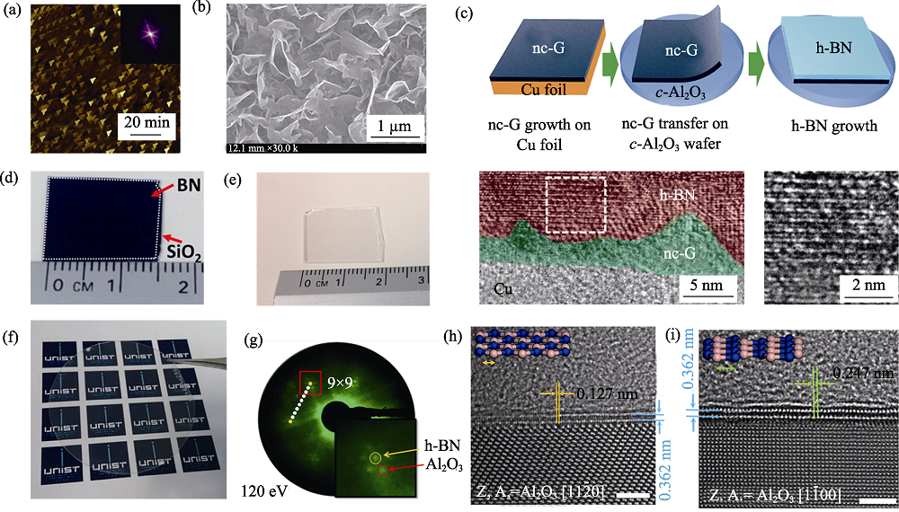
Fig. 1 (a) AFM image of h-BN on SiO2 for 20 min with inset image showing the FFT data[26]; (b) SEM image of the BN sheets grown on Si[27]; (c) Synthesis of h-BN film on sapphire substrate using nc-G and corresponding cross-sectional TEM and HRTEM images[28]; Camera view of h-BN on (d) SiO2 and (e) quartz surface[29,30]; (f) Photograph of EM-h-BN on sapphire substrate; (g) LEED pattern of h-BN grown on sapphire substrate; HR-TEM images of multilayer h-BN grown (h) perpendicular to Al2O3 (11ˉ20) and (i) parallel to Al2O3 (11ˉ20)[31]
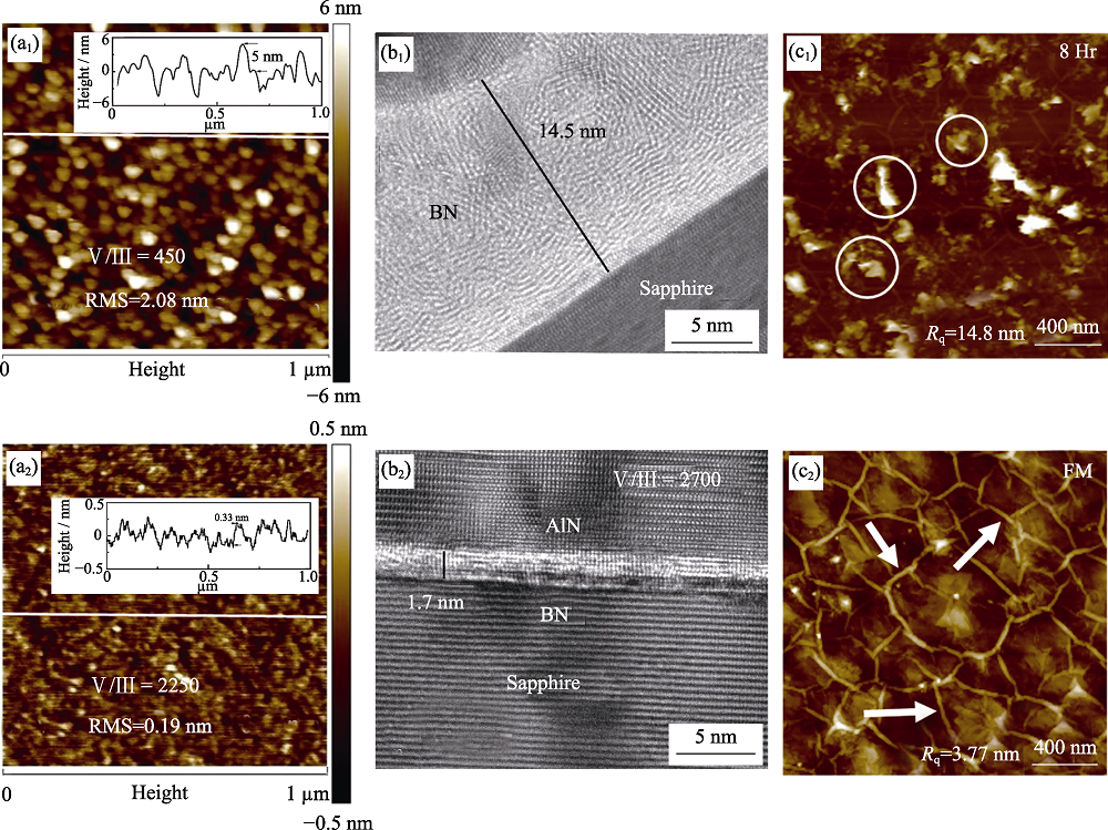
Fig. 2 (a) AFM micrographs with line scans and surface roughness measured on BN films grown at 1000 ℃ for 30 min[35]: (a1) V/III = 450, (a2) V/III = 2250; (b) Cross sectional TEM images of BN layer deposited using (b1) V/III ratio of 450 and (b2) 2700[35]; (c) Surface topography of h-BN films deposited for 8 h (c1) under continuous flow conditions and (c2) using FM scheme[36,37]
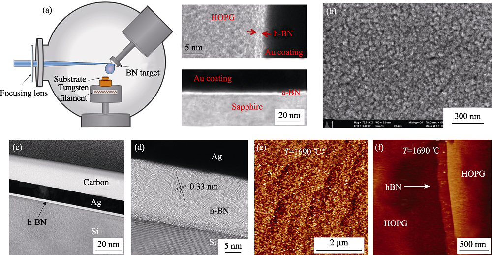
Fig. 3 (a) Schematic of PLD setup and the cross-sectional TEM image of h-BN on HOPG and a-BN on sapphire[42]; (b) High magnification SEM image of an amorphous BN film deposited on sapphire substrate[43]; (c) Cross-sectional TEM image of h-BN film on Si[44]; (d) High-magnification TEM image of the h-BN layered structure on Si[44]; (e-f) AFM images of h-BN grown on (e) sapphire and (f) HOPG for 3 h, 1690 ℃[45]
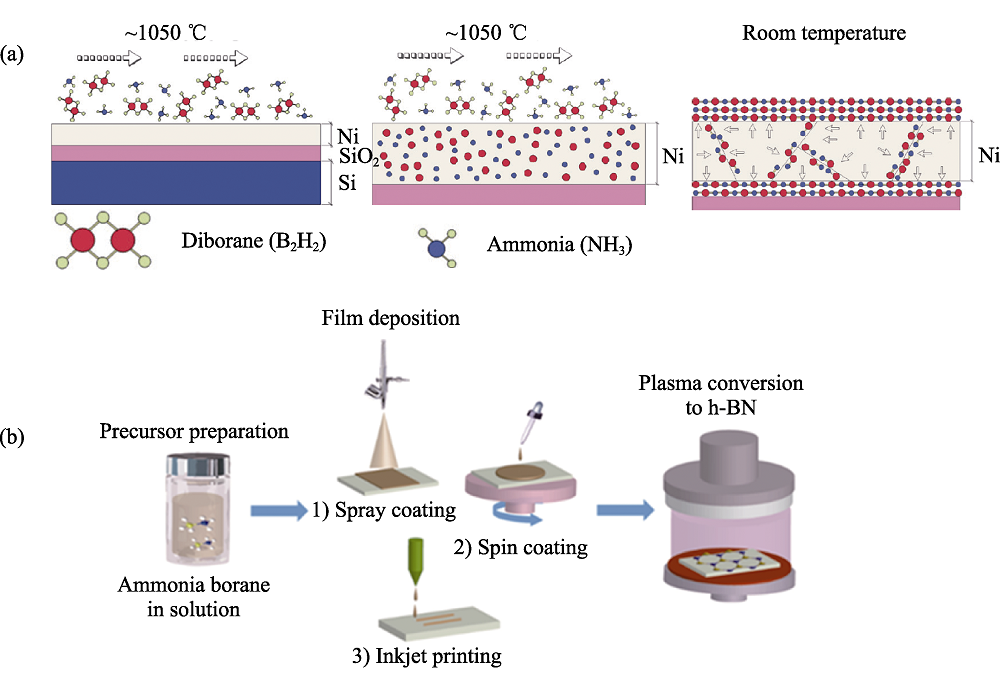
Fig. 4 (a) Growth mechanism of h-BN by diffusion and segregation[47] and (b) schematic illustration of process flow for synthesis of h-BN films by a two-step method[48]
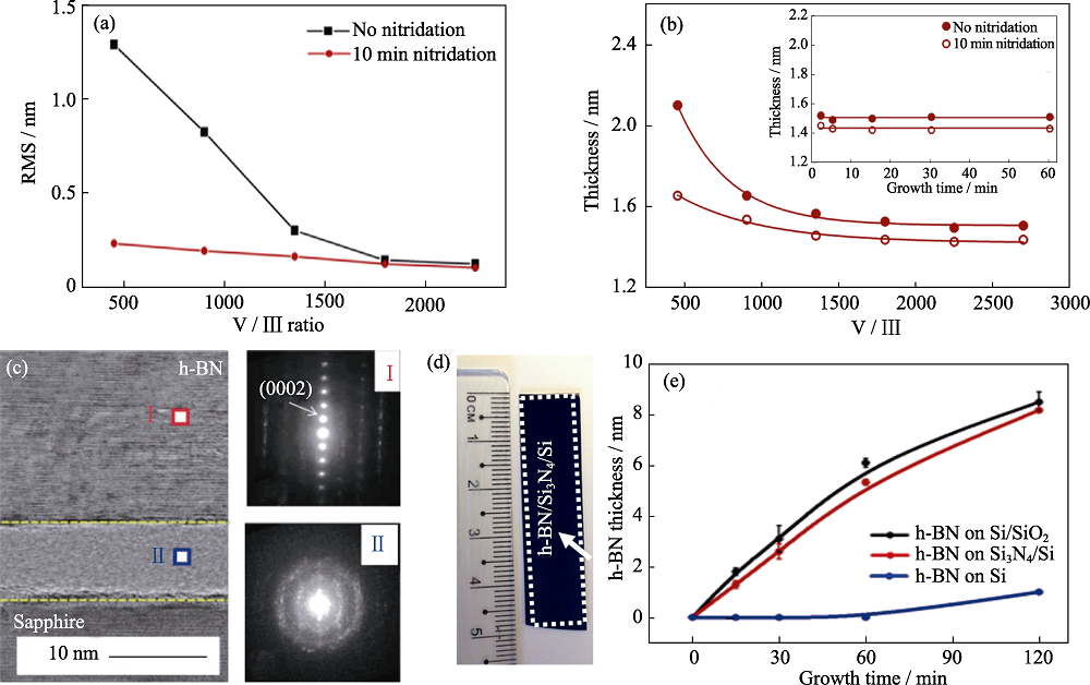
Fig. 5 (a) Plot of RMS determined by AFM vs. V/III; (b) Thickness vs. V/III for BN films grown on sapphire with and without the pre-growth nitridation process with insetshowing thickness vs. growth time for films grown using a V/III ratio of 2250; (c) Cross-sectional STEM image of h-BN grown on sapphire and diffraction patterns for selected areas I and II; (d) Camera view of h-BN on Si3N4/Si; (e) Variations of h-BN film thickness at different CVD growth times for Si3N4/Si, SiO2/Si, and Si substrates[30, 49-53]
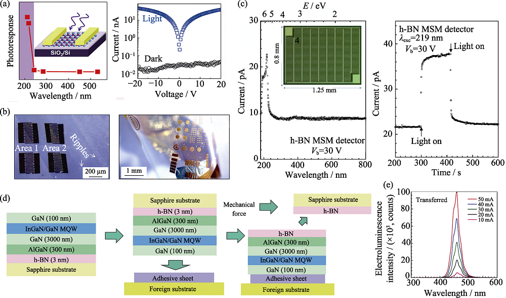
Fig. 6 (a) Response spectrum of the h-BN detector and I-V curves under 212 nm laser irradiation and dark condition[60]; (b) Microscope image of the transferred film and the photograph of the flexible metal-semiconductormetal device[61]; (c) The relative spectral response and photocurrent decay kinetics of h-BN MSM detector measured at Vb = 30 V (Inset showing a microscope image of the h-BN MSM photodetector)[62]; (d) Schematic illustrations of the MQW materials design, release and transfer processes[67]; (e) Electroluminescence spectra from the transferred LED[68]
| [1] | FERRARI A C, BONACCORSO F, FAL´KO V , et al. Science and technology roadmap for graphene, related two-dimensional crystals, and hybrid systems. Nanoscale, 2015,7(11):4598-4810. |
| [2] | TAN C, CAO X, WU X J ,et al. Recent advances in ultrathin two-dimensional nanomaterials. Chem. Rev., 2017,117(9):6225-6331. |
| [3] | GENG D, YANG H Y . Recent advances in growth of novel 2D materials: beyond graphene and transition metal dichalcogenides. Adv. Mater., 2018, 30 (45): 1800865-1-23. |
| [4] | LI L H, CHEN Y . Atomically thin boron nitride unique properties and applications. Adv. Funct. Mater., 2016,26(16):2594-2608. |
| [5] | IZYUMSKAYA N, DEMCHENKO D O, DAS S , et al. Recent development of boron nitride towards electronic applications. Adv. Electron. Mater., 2017,3(5):1600485. |
| [6] | DEAN C R, YOUNG A F, MERIC I , et al. Boron nitride substrates for high-quality graphene electronics. Nat. Nanotech., 2010,5:722-726. |
| [7] | WANG L, MERIC I, HUANG P Y , et al. One-dimensional electrical contact to a two-dimensional material. Science, 2013,324(6158):614-617. |
| [8] | LEE K H, SHIN H J, LEE J , et al. Large-scale synthesis of high-quality hexagonal boron nitride nanosheets for large-area graphene electronics. Nano Lett., 2012,12(2):714-718. |
| [9] | LEE J S, CHOI S H, YUN S J , et al. Wafer-scale single-crystal hexagonal boron nitride film via self-collimated grain formation. Science, 2018,362(6416):817-821. |
| [10] | BRITNELL L, GORBACHEV R V, JALIL R , et al. Field-effect tunneling transistor based on vertical graphene heterostructures. Science, 2012,335(6071):947-950. |
| [11] | WANG H, ZHAO Y. XIE Y , et al. Recent progress in synthesis of two-dimensional hexagonal boron nitride. J. Semicond., 2017,38(3):031003. |
| [12] | KHAN M H, LIU H K, SUN X , et al. Few-atomic-layered hexagonal boron nitride: CVD growth, characterization, and applications. Materials Today, 2017,20(10):611-628. |
| [13] | SUN J, LU C, SONG Y , et al. Recent progress in the tailored growth of two-dimensional hexagonal boron nitride via chemical vapour deposition. Chem. Soc. Rev., 2018,47:4242-4257 . |
| [14] | SONG L, CI L, LU H , et al. Large scale growth and characterization of atomic hexagonal boron nitride layers. Nano Lett., 2010,10(8):3209-3215. |
| [15] | LU G, WU T, YUAN Q , et al. Synthesis of large single-crystal hexagonal boron nitride grains on Cu-Ni alloy. Nat. Commun., 2015, 6: 6160-1-7. |
| [16] | CANEVA S, WEATHERUP R S, BAYER B C , et al. Nucleation control for large, single crystalline domains of monolayer hexagonal boron nitride via Si-doped Fe catalysts. Nano Lett., 2015,15(3):1867-1875. |
| [17] | JI Y, CALDERON B, HAN Y , et al. Chemical vapor deposition growth of large single-crystal mono-, bi-, tri-layer hexagonal boron nitride and their interlayer stacking. ACS Nano, 2017,11(12):12057-12066. |
| [18] | LIU L, SIEGEL D A, CHEN W , et al. Unusual role of epilayer- substrate interactions in determining orientational relations in van der Waals epitaxy. Proc. Natl. Acad. Sci. USA, 2014,111(47):16670-16675. |
| [19] | YIN J, LIU X F, LU W L , et al. Aligned growth of hexagonal boron nitride monolayer on germanium. Small, 2015,11(40):5375-5380. |
| [20] | WANG H L, ZHANG X W, LIU H , et al. Synthesis of large-sized single-crystal hexagonal boron nitride domains on nickel foils by ion beam sputtering deposition. Adv. Mater., 2015,27(48):8109-8115. |
| [21] | MENG J H, ZHANG X W, WANG Y , et al. Aligned growth of millimeter-size hexagonal boron nitride single-crystal domains on epitaxial nickel thin film. Small, 2017, 13(18): 1604179-1-8. |
| [22] | MENG J H, MING B M, ZHANG X W , et al. Controlled growth of unidirectionally aligned hexagonal boron nitride domains on single crystal Ni (111)/MgO thin films. Cryst. Growth Des., 2019,19(1):453-459. |
| [23] | OH H, JO J, TCHOE Y , et al. Centimeter-sized epitaxial h-BN films. NPG Asia Materials, 2016,8:e330. |
| [24] | KIM K, CHOI J Y, KIM T , et al. A role for graphene in silicon- based semiconductor devices. Nature, 2011,479:338-344. |
| [25] | TAY R Y, TSANG S H, LOEBLEIN M , et al. Direct growth of nanocrystalline hexagonal boron nitride films on dielectric substrates. Appl. Phys. Lett., 2015, 106(10): 101901-1-5. |
| [26] | WU Q, LEE J, SUN J , et al. In situ direct growth of graphene/ hexagonal boron nitride heterostructure on SiO2 substrate without metal catalyst. Carbon, 2018,138:76-80. |
| [27] | QIN L, YU J, LI M , et al. Catalyst-free growth of mono- Catalyst-free growth of mono- and few-atomic-layer boron nitride sheets by chemical vapor deposition. Nanotechnology, 2011, 22(21): 215602-1-7. |
| [28] | LEE K H, SHIN H J, KUMAR B , et al. Nanocrystalline graphene tailored hexagonal boron nitride thin films. Angew. Chem. Int. Ed., 2014,53(43):11493-11497. |
| [29] | CHEN Y, LIANG H, XIA X , et al. Growth temperature impact on film quality of hBN grown on Al2O3 using non-catalyzed borazane CVD. J. Mater. Sci.: Mater. Electron., 2017,28(19):14341-14347. |
| [30] | BEHURA S, NGUYEN P, CHE S , et al. Large-area, transfer-free, oxide-assisted synthesis of hexagonal boron nitride films and their heterostructures with MoS2 and WS2. J. Am. Chem. Soc, 2015,137(40):13060-13065. |
| [31] | JANG A R, HONG S, HYUN C , et al. Wafer-scale and wrinkle- free epitaxial growth of single-orientated multilayer hexagonal boron nitride on sapphire. Nano Lett., 2016,16(5):3360-3366. |
| [32] | CHUBAROV M, PEDERSEN H, HÖGBERG H , et al. Growth of high quality epitaxial rhombohedral boron nitride. Cryst. Growth Des., 2012,12(6):3215-3220. |
| [33] | PADUANO Q S, SNURE M, BONDY J , et al. Self-terminating growth in hexagonal boron nitride by metal organic chemical vapor deposition. Appl. Phys. Express, 2014, 7(7): 071004-1-4. |
| [34] | PADUANO Q, SNURE M, WEYBURNE D , et al. Metalorganic chemical vapor deposition of few-layer sp2 bonded boron nitride films. J. Cryst. Growth, 2016,449:148-155. |
| [35] | VANGALA S, SIEGEL G, PRUSNICK T , et al. Wafer scale BN on sapphire substrates for improved grapheme transport. Sci. Rep., 2018, 8(1): 8842-1-9. |
| [36] | YANG X, NITTA S, NAGAMATSU K , et al. Growth of hexagonal boron nitride on sapphire substrate by pulsed-mode metalorganic vapor phase epitaxy. J. Cryst. Growth, 2018,482:1-8. |
| [37] | CHUGH D, LEUNG J W, LI L , et al. Flow modulation epitaxy of hexagonal boron nitride. 2D Mater., 2018, 5(4): 045018-1-10. |
| [38] | RICE A, ALLERMAN A, CRAWFORD M , et al. Effects of deposition temperature and ammonia flow on metal-organic chemical vapor deposition of hexagonal boron nitride. J. Cryst. Growth, 2018,485:90-95. |
| [39] | LI X, SUNDARAM S, GMILI Y E , et al. Large-area two-dimensional layered hexagonal boron nitride grown on sapphire by metalorganic vapor phase epitaxy. Cryst. Growth Des., 2016,16(6):3409-3415. |
| [40] | SUTTER P, LAHIRI J, ZAHL P , et al. Scalable synthesis of uniform few-layer hexagonal boron nitride dielectric Films. Nano Lett., 2013,13(1):276-281. |
| [41] | WANG H L, ZHANG X W, MENG J H , et al. Controlled growth of few-layer hexagonal boron nitride on copper foils using ion beam sputtering deposition. Small, 2015,11(13):1542-1547. |
| [42] | GLAVIN N R, JESPERSEN M L, CHECK M H , et al. Synthesis of few-layer, large area hexagonal-boron nitride by pulsed laser deposition. Thin Solid Films, 2014,572:245-250. |
| [43] | STEWART D M, LAD R J . Enhanced crystallinity of h-BN films induced by substrate bias during magnetron sputtering. Phys. Status Solidi B, 2017, 255(3): 1700458-1-5. |
| [44] | PARK H, KIM T K, CHO S W , et al. Large-scale synthesis of uniform hexagonal boron nitride films by plasma-enhanced atomic layer deposition. Sci. Rep., 2017, 7: 40091-1-8. |
| [45] | VUONG T Q P, CASSABOISs G, VALVIN P , et al. Deep ultraviolet emission in hexagonal boron nitride grown by high-temperature molecular beam epitaxy. 2D Mater., 2017, 4(2): 021023-1-7. |
| [46] | BRESNEHAN M S, HOLLANDER M J, WETHERINGTON M , et al. Prospects of direct growth boron nitride films as substrates for graphene electronics. J. Mater. Res., 2014,29(3):459-471. |
| [47] | SONDE S, DOLOCAN A, LU N , et al. Ultrathin, wafer-scale hexagonal boron nitride on dielectric surfaces by diffusion and segregation mechanism. 2D Mater., 2017, 4(2): 025052-1-10. |
| [48] | LIU T, PREMASIRI K, SUI Y , et al. Direct, transfer-free growth of large-area hexagonal boron nitride films by plasma-enhanced chemical film conversion (PECFC) of printable, solution-processed ammonia borane. ACS Appl. Mater. Interfaces, 2018,10(50):43936-43945. |
| [49] | SNURE M, PADUANO Q, KIEFER A . Effect of surface nitridation on the epitaxial growth of few-layer sp2 BN. J. Cryst. Growth, 2014,436:16-22. |
| [50] | AHMED K, DAHAL R, WELTZ A , et al. Effects of sapphire nitridation and growth temperature on the epitaxial growth of hexagonal boron nitride on sapphire. Mater. Res. Express, 2017, 4(1): 015007-1-6. |
| [51] | YANG X, NITTA S, PRISTOVSEK M , et al. Interface amorphization in hexagonal boron nitride films on sapphire substrate grown by metalorganic vapor phase epitaxy. Appl. Phys. Express, 2018, 11(5): 051002-1-4. |
| [52] | SUNDARAM S, LI X, ALAM S , et al. Wafer-scale MOVPE growth and characterization of highly ordered h-BN on patterned sapphire substrates. J. Cryst. Growth, 2019,509:40-43. |
| [53] | BEHURA S, NGUYEN P, DEBBARMA R , et al. Chemical interaction- guided, metal-free growth of large-area hexagonal boron nitride on silicon-based substrates. ACS Nano, 2017,11(5):4985-4994. |
| [54] | LI Q, WU Q, GAO J , et al. Direct growth of 5 in. uniform hexagonal boron nitride on glass for high-performance deep-ultraviolet light-emitting diodes. Adv. Mater. Interfaces, 2018, 5(18): 1800662-1-8. |
| [55] | MAJETY S, LI J, ZHAO W P , et al. Hexagonal boron nitride and 6H- SiC heterostructures. Appl. Phys. Lett., 2013, 102(21): 213505-1-4. |
| [56] | SHIN H C, JANG Y, KIM T H , et al. Epitaxial growth of a single- crystal hybridized boron nitride and graphene layer on a wide-band gap semiconductor. J. Am. Chem. Soc., 2015,137(21):6897-6905. |
| [57] | WANG X B, WENG Q H, WANG X , et al. Biomass-directed synthesis of 20 g high-quality boron nitride nanosheets for thermoconductive polymeric composites. ACS Nano, 2014,8(9):9081-9088. |
| [58] | OROFEO C M, SUZUKI S, HIBINO H . Ultrathin chemical vapor deposition (CVD)-grown hexagonal boron nitride as a high-quality dielectric for tunneling devices on rigid and flexible substrates. J. Phys. Chem. C, 2014,118(6):3340-3346. |
| [59] | CHUANG H J, CHAMLAGAIN B, KOEHLER M , et al. Low-resistance 2D/2D ohmic contacts: a universal approach to high-performance WSe2, MoS2, and MoSe2 transistors. Nano Lett., 2016,16(3):1896-1902. |
| [60] | LIU H, MENG J, ZHANG X , et al. High-performance deep ultraviolet photodetectors based on few-layer hexagonal boron nitride. Nanoscale, 2018,10(12):5559-5565. |
| [61] | LI X, JORDAN M B, AYARI T , et al. Flexible metal- semiconductor-metal device prototype on waferscale thick boron nitride layers grown by MOVPE. Sci. Rep., 2017, 7(1): 786-1-8. |
| [62] | LI J, MAJETY S, DAHAL R , et al. Dielectric strength, optical absorption, and deep ultraviolet detectors of hexagonal boron nitride epilayers. Appl. Phys. Lett., 2012, 101(17): 171112-1-4. |
| [63] | AHMED K, DAHAL R, WELTZ A , et al. Growth of hexagonal boron nitride on (111) Si for deep UV photonics and thermal neutron detection. Appl. Phys. Lett., 2016, 109(11): 113501-1-4. |
| [64] | THANH D T, JIN J, KO K B , et al. Hexagonal boron nitride pattern embedded in AIN template layer for visible-blind ultraviolet photodetectors. Opt. Mater. Express, 2017,7(5):1463-1472. |
| [65] | WU Q, YAN J, ZHANG L , et al. Growth mechanism of AlN on hexagonal BN/sapphire substrate by metal-organic chemical vapor deposition. Cryst. Eng. Comm., 2017,19(39):5849-5856. |
| [66] | WU Q, GUO Y, SUNDARAM S , et al. Exfoliation of AlN film using two-dimensional multilayer hexagonal BN for deep-ultraviolet light-emitting diodes. Appl. Phys. Express, 2019, 12(1): 015505-1-5. |
| [67] | KOBAYASHI Y, KUMAKURA K, AKASAKA T , et al. Layered boron nitride as a release layer for mechanical transfer of GaN-based devices. Nature, 2012,484:223-227. |
| [68] | SUNDARAM S, LI X, ALAM S , et al. MOVPE van der Waals epitaxial growth of AlGaN/AlGaN multiple quantum well structures with deep UV emission on large scale 2D h-BN buffered sapphire substrates. J. Cryst. Growth, 2019,507:352-356. |
| [1] | CHEN Mingjun, MIAO Hongkang, XIAO Yingjun, DENG Jianbo, ZHANG Xiang, ZHAO Jiupeng, LI Yao. Photo- and Thermo-chromic Dual-responsive Materials: A Review on Design Strategies and Applications in Smart Windows [J]. Journal of Inorganic Materials, 2026, 41(6): 723-738. |
| [2] | SONG Kunjie, XIE Rongjun. Research Advances on Machine Learning-driven Development of Novel Luminescent Materials [J]. Journal of Inorganic Materials, 2026, 41(6): 689-703. |
| [3] | HU Yuqing, ZHU Yixin, LE Xianhao, WAN Qing. Lithium Tantalate Wafer: Advances in Thinning Technology and Application in Pyroelectric Infrared Detectors [J]. Journal of Inorganic Materials, 2026, 41(6): 764-774. |
| [4] | LIU Chunfan, CHEN Ke, GE Fangfang, HUANG Qing. Research Progress on Lead-bismuth Eutectic Corrosion Resistant Coatings [J]. Journal of Inorganic Materials, 2026, 41(6): 775-786. |
| [5] | HU Yang, XIE Min, ZHANG Xiaoyi, LI Xiang, GUO Xinwei, JIANG Nan, ZHOU Wenhan, ZHANG Shengli, ZENG Haibo. Research Progress on Computational and Data-driven Environmental-friendly Luminescent Materials [J]. Journal of Inorganic Materials, 2026, 41(6): 704-722. |
| [6] | WANG Junbu, HUANG Zeai, YANG Mingkai, MENG Ying, ZHOU Mingwei, ZHOU Ying. Research Progress on Anti-coking Catalytic Materials for Methane Conversion [J]. Journal of Inorganic Materials, 2026, 41(6): 739-750. |
| [7] | WANG Jinwen, YANG Zhen, ZHOU Huan, XIA Dan, YANG Lei. Biomedical Applications of Injectable Inorganic Biomaterials [J]. Journal of Inorganic Materials, 2026, 41(6): 751-763. |
| [8] | LI Hantao, SHEN Qiang, LUO Guoqiang, WANG Xuefei, GAO Ming, CHEN Chen. Research Progress on Structure and Performance Regulation of Silicon-based Anode Materials via Mechanical Ball Milling [J]. Journal of Inorganic Materials, 2026, 41(5): 561-572. |
| [9] | XIE Chenyi, MIAO Huaming, ZHANG Weiran, LIU Rongjun, WANG Yanfei, LI Duan. Research Progress on Theoretical Calculation in the Field of High-entropy Ceramics [J]. Journal of Inorganic Materials, 2026, 41(5): 545-560. |
| [10] | LI Xuan, YE Kuicai, FENG Jiayin, QIU Jiajun, QIAN Wenhao, XING Min. Surface Modification of Titanium-based Dental Implants for Soft Tissue Sealing: A Review [J]. Journal of Inorganic Materials, 2026, 41(4): 432-444. |
| [11] | PENG Dezhao, LI Rui, WANG Wenhong, WANG Zirui, ZHANG Zhizhen. Research Progress on Sodium Chloride Solid Electrolytes [J]. Journal of Inorganic Materials, 2026, 41(4): 409-420. |
| [12] | CHEN Kun, JIANG Yonggang, FENG Junzong, LI Liangjun, HU Yijie, FENG Jian. Research Progress on Lanthanum Zirconate Porous Materials for Thermal Insulation [J]. Journal of Inorganic Materials, 2026, 41(4): 421-431. |
| [13] | WEI Lianjin, QI Zhijie, WANG Xin, ZHU Junwu, FU Yongsheng. Modification of Nanodiamond and Its Application in Electrocatalytic Oxygen Reduction Reaction [J]. Journal of Inorganic Materials, 2026, 41(3): 273-288. |
| [14] | LIU Zhanyi, LI Mian, OUYANG Xiaoping, CHAI Zhifang, HUANG Qing. Recent Progress on Removal of Sr/Cs from Molten Salt in Dry Reprocessing [J]. Journal of Inorganic Materials, 2026, 41(2): 150-158. |
| [15] | SUN Lian, ZHANG Leilei, XUE Zexu, WU Kun, CHEN Ye, LI Zhiyuan, WANG Lukai, WANG Zungang. Research Progress on Zero-dimensional Metal Halide Scintillators towards Radiation Detection Applications [J]. Journal of Inorganic Materials, 2026, 41(2): 159-176. |
| Viewed | ||||||
|
Full text |
|
|||||
|
Abstract |
|
|||||