Journal of Inorganic Materials ›› 2019, Vol. 34 ›› Issue (9): 909-917.DOI: 10.15541/jim20180587
WANG Yang,ZHU Jia-Qi( ),HU Zhong-Bo,DAI Bing
Received:2018-12-17
Revised:2019-02-12
Published:2019-09-20
Online:2019-05-29
Supported by:CLC Number:
WANG Yang, ZHU Jia-Qi, HU Zhong-Bo, DAI Bing. Heteroepitaxial Growth of Single Crystal Diamond Films on Iridium: Procedure and Mechanism[J]. Journal of Inorganic Materials, 2019, 34(9): 909-917.
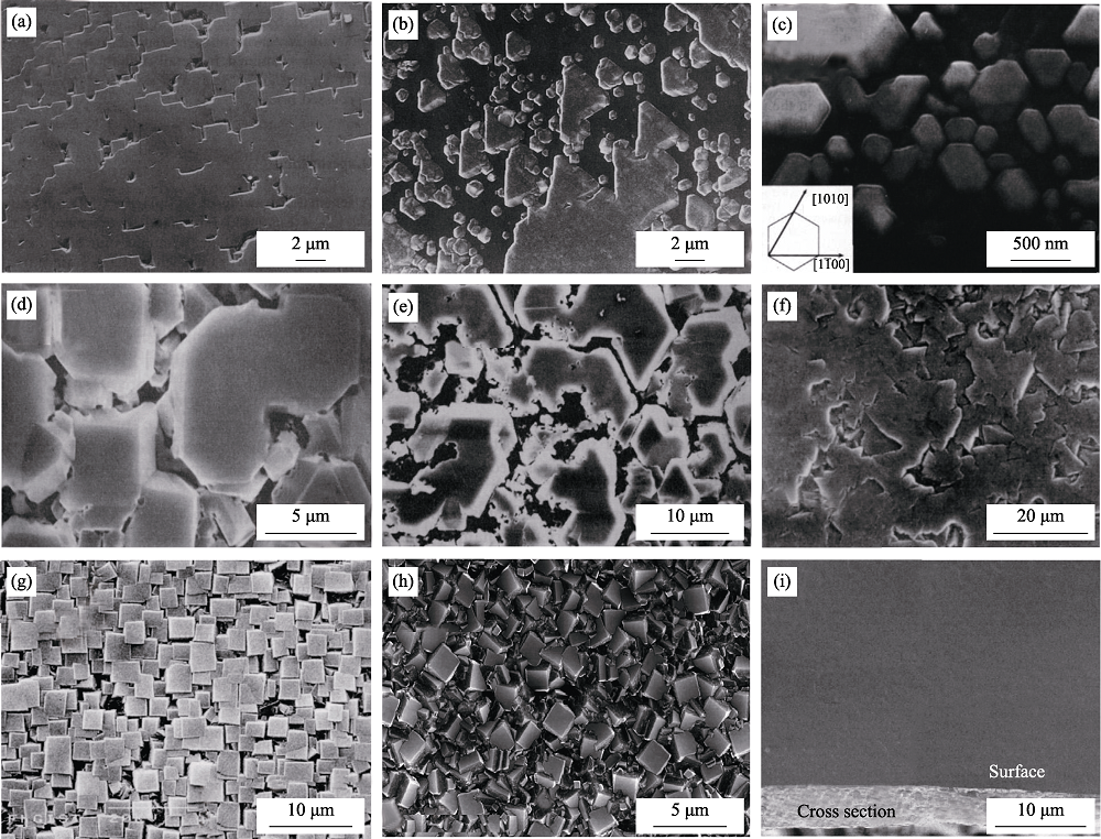
Fig. 1 Heteroepitaxial diamond growth on different substrate materials[32,33,34] (a) c-BN(001); (b) c-BN(111); (c) Al2O3(0001); (d) Ni(001); (e) Ni(111); (f) Pt(111); (g) Si(001); (h) 4H-SiC(001); (i) Ir(001)
| Bottom substrate | Structure | Thickness | Quality | Ref. |
|---|---|---|---|---|
| Metal oxide (MO) | MgO(100)/Ir(100)/diamond(100) | 50 μm | tilt0.16° | [42, 47] |
| SrTiO3(100)/Ir(100)/diamond(100) | 34 μm | tilt0.17° twist0.38° | [48] | |
| Al2O3(11ˉ20)/Ir(100)/diamond(100) | 38 μm | tilt~0.30° | [49] | |
| Si | Si(100)/MgO(100)/Ir(100)/diamond(100) | 8 μm | tilt0.88° twist4.13° | [50] |
| Si(100)/YSZ(100)/Ir(100)/diamond(100) | 1.60 mm | tilt0.18° twist0.29° | [16, 51] | |
| Si(100)/SrTiO3(100)/Ir(100)/diamond(100) | 350 μm | tilt0.38° twist0.98° | [52] | |
| Si(100)/CaF2(100)/Ir(100)/diamond(100) | - | tilt0.61° | [53] |
Table 1 Quality of diamond grown on different layer structures based on Ir(100) substrate
| Bottom substrate | Structure | Thickness | Quality | Ref. |
|---|---|---|---|---|
| Metal oxide (MO) | MgO(100)/Ir(100)/diamond(100) | 50 μm | tilt0.16° | [42, 47] |
| SrTiO3(100)/Ir(100)/diamond(100) | 34 μm | tilt0.17° twist0.38° | [48] | |
| Al2O3(11ˉ20)/Ir(100)/diamond(100) | 38 μm | tilt~0.30° | [49] | |
| Si | Si(100)/MgO(100)/Ir(100)/diamond(100) | 8 μm | tilt0.88° twist4.13° | [50] |
| Si(100)/YSZ(100)/Ir(100)/diamond(100) | 1.60 mm | tilt0.18° twist0.29° | [16, 51] | |
| Si(100)/SrTiO3(100)/Ir(100)/diamond(100) | 350 μm | tilt0.38° twist0.98° | [52] | |
| Si(100)/CaF2(100)/Ir(100)/diamond(100) | - | tilt0.61° | [53] |
| Nucleation process | Primary growth | Rapid growth | |||
|---|---|---|---|---|---|
| H2 cleaning | H2/CH4 stabilization | BEN | |||
| CH4/% | 0(Pure H2) | 4 | 4 | 0.6 | 5 |
| Pressure/(×103, Pa) | 2 | 2 | 2 | 2 | 20 |
| Power/W | 400 | 400 | 400 | 400 | 3000 |
| Bias voltage/V | 0 | 0 | -307 | 0 | 0 |
| Substrate temperature/℃ | (600±50) | (650±50) | (700±50) | (600±50) | (880±30) |
| Duration/min | 10 | 10 | 40-45 | 30 | Up to 48 h |
Table 2 Experimental conditions for Bias Enhanced Nucleation (BEN) and growth of diamond on iridium[59]
| Nucleation process | Primary growth | Rapid growth | |||
|---|---|---|---|---|---|
| H2 cleaning | H2/CH4 stabilization | BEN | |||
| CH4/% | 0(Pure H2) | 4 | 4 | 0.6 | 5 |
| Pressure/(×103, Pa) | 2 | 2 | 2 | 2 | 20 |
| Power/W | 400 | 400 | 400 | 400 | 3000 |
| Bias voltage/V | 0 | 0 | -307 | 0 | 0 |
| Substrate temperature/℃ | (600±50) | (650±50) | (700±50) | (600±50) | (880±30) |
| Duration/min | 10 | 10 | 40-45 | 30 | Up to 48 h |
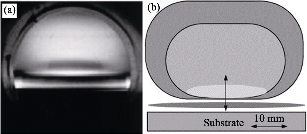
Fig. 2 Changes in the shape of plasma ball after application of bias voltage[57] (a) Photograph; (b) Schematic
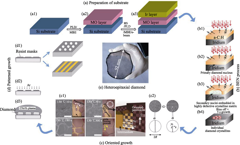
Fig. 3 Procedure of single diamond eptaxial growth on Ir substrate[16, 60-64] (a) Preparation of substrate; (b) Bias Enhanced Nucleation (BEN) process; (c) Oriented growth; (d) Patterned growth; (e) Heteroepitaxial diamond MS: Megnetron Sputtering; PLD: Pulsed Laser Deposition; MBE: Molecular Beam Epitaxy
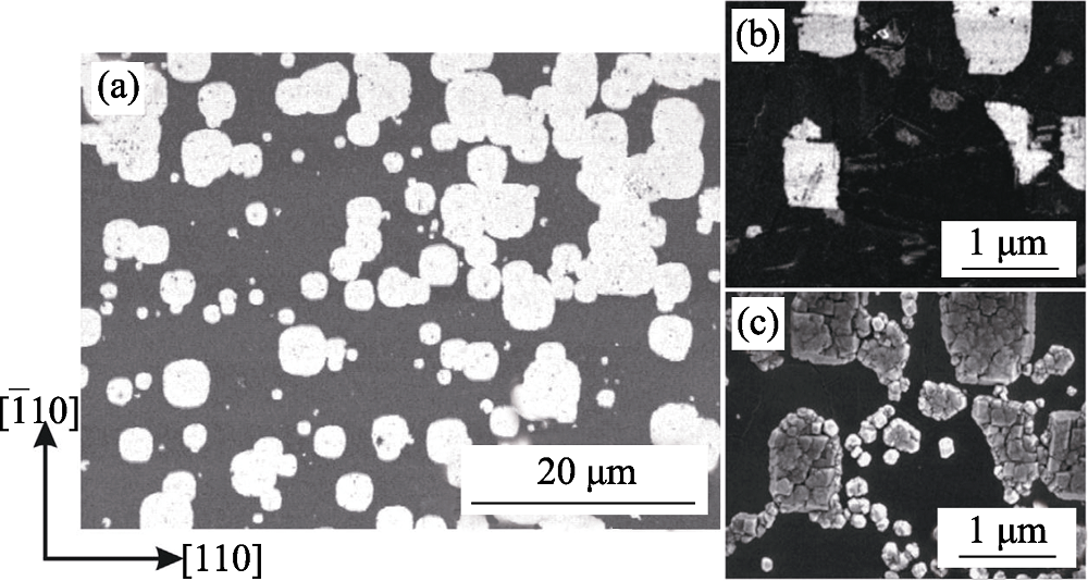
Fig. 4 SEM images[72] of the iridium surface after BEN treatment (a), local spots after BEN (b) and after a subsequent growth step (c)
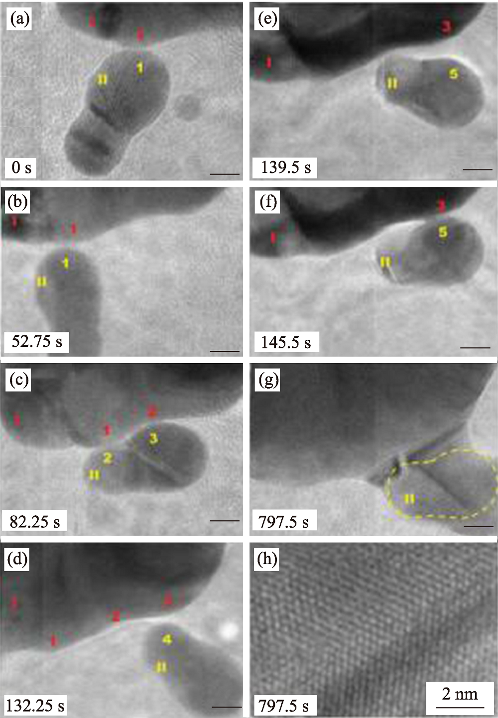
Fig. 5 (a-g) Sequence of TEM images showing typical dynamics of the attachment process, with surfaces of particles I and II enabling transient contact at many points and orientations before finally attaching and growing together; (h) High-resolution image of interface in (g)[77]
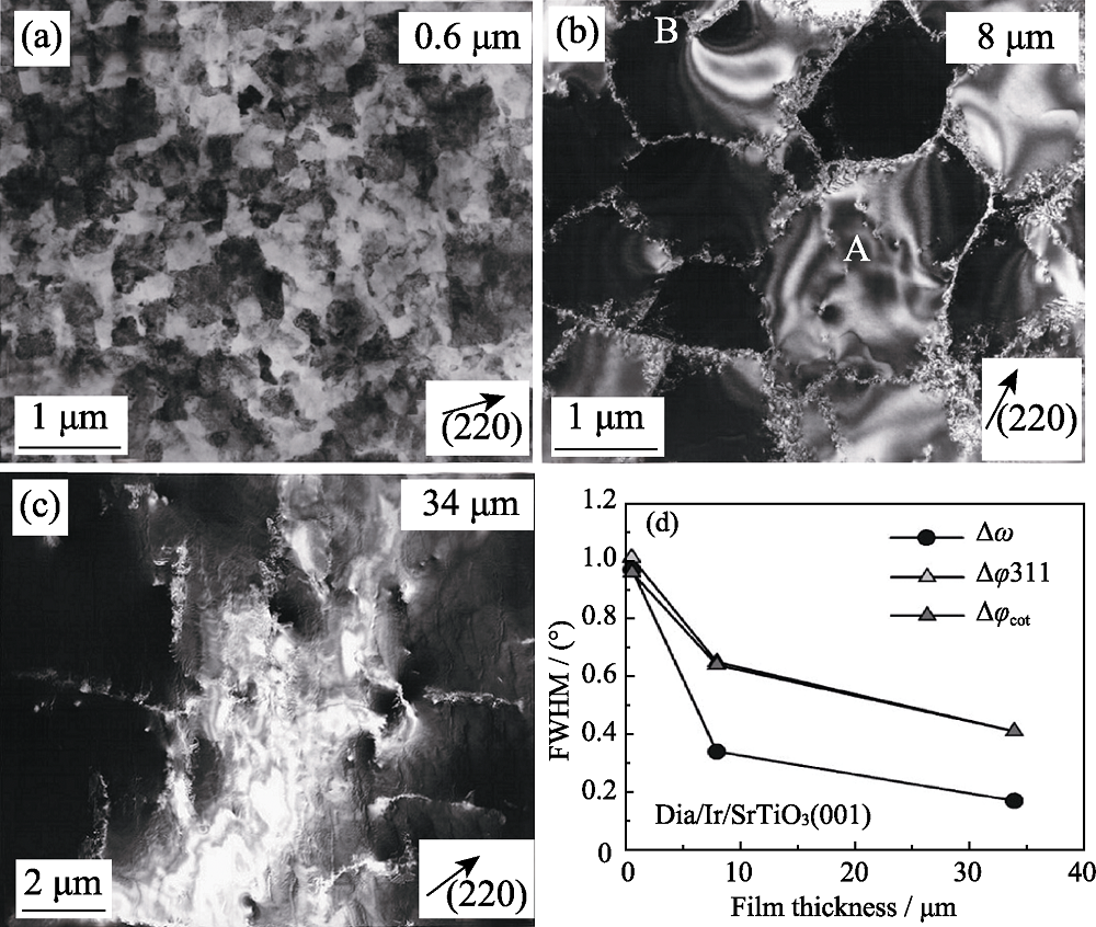
Fig. 6 Heteroepitaxial diamond films on Ir/SrTiO3(100)[48] (a-c) TEM images; (d) Reduction in mosaic spreaded with increasing thickness
| [1] | ZOU L, ZHOU M . Experimental investigation and numerical simulation on interfacial carbon diffusion of diamond tool and ferrous metals. Journal of Wuhan University of Technology-Materials Science Edition, 2016,31(2):307-314. |
| [2] | ZHANG C, WANG R, CAI Z ,et al. Low-temperature densification of diamond/Cu composite prepared from dual-layer coated diamond particles. Journal of Materials Science Materials in Electronics, 2015,26(1):185-190. |
| [3] | NAZARI M, HANCOCK B L, ANDERSON J ,et al. Optical characterization and thermal properties of CVD diamond films for integration with power electronics. Solid-State Electronics, 2017,136(10):12-17. |
| [4] | ZHU D, BANDY J A, LI S ,et al. Amino-terminated diamond surfaces: photoelectron emission and photocatalytic properties. Surface Science, 2016,650(8):295-301. |
| [5] | SHEN H J, WANG L J, HUANG J ,et al. Research for (100)-oriented diamond film radiation detector. Journal of Inorganic Materials, 2009,24(6):1254-1258. |
| [6] | WILLIAMS T, MARTENS A, CASSOU K ,et al. Novel applications and future perspectives of a fast diamond gamma ray detector. Nuclear Instruments and Methods in Physics Research A, 2017,845(5):199-202. |
| [7] | ZHANG R, ZHAO W S, YIN W Y ,et al. Impacts of diamond heat spreader on the thermo-mechanical characteristics of high-power AlGaN/GaN HEMTs. Diamond and Related Materials, 2015,52(2):25-31. |
| [8] | DING M Q, LI L, DU Y ,et al. Development of an extremely thin-diamond window for terahertz traveling wave tubes. Diamond and Related Materials, 2017,79(10):173-178. |
| [9] | WANG J J, HE Z Z, YU C ,et al. Comparison of field-effect transistors on polycrystalline and single-crystal diamonds. Diamond and Related Materials, 2016,70(11):114-117. |
| [10] | KASU M . Diamond epitaxy: basics and applications. Progress in Crystal Growth and Characterization of Materials, 2016,62(2):317-328. |
| [11] | KUPRIYANOV I N, KHOKHRYAKOV A F, BORZDOV Y M ,et al. HPHT growth and characterization of diamond from a copper- carbon system. Diamond and Related Materials, 2016,69(10):198-206. |
| [12] | XIAO H Y, LI S S, QIN Y K ,et al. Studies on synthesis of boron- doped Gem-diamond single crystals under high temperature and high presure. Acta Physica Sinica, 2014,63(19):198101. |
| [13] | MOKUNO Y, CHAYAHARA A, YAMADA H ,et al. Improving purity and size of single-crystal diamond plates produced by high-rate CVD growth and lift-off process using ion implantation. Diamond and Related Materials, 2009,18(10):1258-1261. |
| [14] | YAMADA H, CHAYAHARA A, MOKUNO Y ,et al. Effects of crystallographic orientation on the homoepitaxial overgrowth on tiled single crystal diamond clones. Diamond and Related Materials, 2015,57(8):17-21. |
| [15] | YAMADA H, CHAYAHARA A, MOKUNO Y ,et al. Uniform growth and repeatable fabrication of inch-sized wafers of a single- crystal diamond. Diamond and Related Materials, 2013,33(3):27-31. |
| [16] | SCHRECK M, GSELL S, BRESCIA R , et al. Ion bombardment induced buried lateral growth: the key mechanism for the synthesis of single crystal diamond wafers. Scientific Reports, 2017, 7: 44462-1-3. |
| [17] | 朱金凤 . 微波CVD法制备高质量金刚石颗粒. 武汉: 武汉工程大学硕士学位论文, 2013. |
| [18] | 张景文, 陈旭东, 王进军 , 等. 一种基于异质外延生长单晶金刚石的方法. 中国, C30B25/18, CN201710633557. 2017.07.28. |
| [19] | LI Y F, SHE J M, SU J J ,et al. Heteroepitaxial nucleation of diamond on Ir(100)/MgO(100) substrate by bias enhanced microwave plasma chemical vapor deposition method. Journal of Synthetic Crystals, 2015,44(4):896-901. |
| [20] | 王杨, 代兵, 朱嘉琦 , 等. 一种异质外延生长大尺寸单晶金刚石的衬底及其制备方法. 中国, C30B29/04, CN201410794743.0. 2015.04.08. |
| [21] | SARTORI A, FISCHER M, GSELL S ,et al. In situ boron doping during heteroepitaxial growth of diamond on Ir/YSZ/Si. Physica Status Solidi A-Applications and Materials Science, 2012,209(9):1643-1650. |
| [22] | LIAO K J, WANG W L, FENG B . Effect of nucleation rate on heteroepitaxial diamond growth on Si (100) via electron-emission- enhanced nucleation by hot filament chemical vapor deposition. Physica Status Solidi A-Applications and Materials Science, 1998,167(1):117-123. |
| [23] | ZHAO S, HUANG J, ZHOU X ,et al. Highly dispersible diamond nanoparticles for pretreatment of diamond films on Si substrate. Applied Surface Science, 2018,434(3):260-264. |
| [24] | LIU C, WANG J H, WENG J . Preparation of the high-quality highly (100) oriented diamond films with controllable growth. Acta Physica Sinica, 2015,64(2):028101. |
| [25] | GAO F, JIA X P, MA H A ,et al. Hetero-epitaxial diamond single crystal growth on surface of cBN single crystals at high pressure and high temperature. Chinese Physics Letters, 2008,25(6):2273-2276. |
| [26] | WANG C X, GAO C X, ZHANG T C . Preparation of p-n junction diode by B-doped diamond film grown on Si-doped c-BN. Chinese Physics Letters, 2002,19(10):1513-1515. |
| [27] | HAYASHI Y, MATSUSHITA Y, SOGA T ,et al. The formation of a (111) texture of the diamond film on Pt/TiO2/SiOx/Si substrate by microwave plasma chemical vapor deposition. Diamond and Related Materials, 2002,11(3-6):499-503. |
| [28] | SITAR Z, LIU W, YANG P C ,et al. Heteroepitaxial nucleation of diamond on nickel. Diamond and Related Materials, 1998,7(2):276-282. |
| [29] | ITO S, NAGAI M, MATSUMOTO T ,et al. Self-separation of freestanding diamond films using graphite interlayers precipitated from C-dissolved Ni substrates. Journal of Crystal Growth, 2017,470(14):104-107. |
| [30] | HE X C, SHEN H S, ZHANG Z M ,et al. Growth of CVD heteroepitaxial diamond on silicon (001) and its electronic properties. Diamond and Related Materials, 2000,9(9):1626-1631. |
| [31] | CHANG L, LIN T S, CHEN J L ,et al. Transmission electron microscopy study of diamond nucleation on 6HSiC single crystal with possibility of epitaxy. Applied Physics Letters, 1993,62(26):3444-3446. |
| [32] | SCHRECK M . CVD Diamond for Electronic Devices and Sensors. Chichester: Wiley, 2009: 125-161. |
| [33] | MOORE E, JARRELL J, CAO L . Heteroepitaxial diamond growth on 4H-SiC using microwave plasma chemical vapor deposition. Heliyon, 2017,3(9):e00404. |
| [34] | SCHRECK M, SCHURY A, HÖRMANN F , et al. Mosaicity reduction during growth of heteroepitaxial diamond films on iridium buffer layers: experimental results and numerical simulations. Journal of Applied Physics, 2002,91(2):676-685. |
| [35] | VERSTRAETE M J, CHARLIER J C . Why is iridium the best substrate for single crystal diamond growth? Applied Physics Letters, 2005,86(191):191917. |
| [36] | 野口仁 . 金刚石膜的制造方法. 日本, C30B25/10, CN201510627462.0. 2015.12.23. |
| [37] | MARTOVITSKY V P, EVLASHIN S A, SUETIN N V , et al. Heteroepitaxial Ir layers on diamond. Journal of Physics D-Applied Physics, 2011, 44(21): 21540-1-6. |
| [38] | MEYER F, OESER S, GRAFF A ,et al. Effect of substrate bias on the growth behavior of iridium on A-plane sapphire using radio frequency sputtering at low temperatures. Thin Solid Films, 2018,650(3):65-70. |
| [39] | FAN L, JACOBS C B, ROULEAU C M ,et al. Stabilizing Ir(001) epitaxy on yttria-stabilized zirconia using a thin Ir seed layer grown by pulsed laser deposition. Crystal Growth & Design, 2017,17(1):89-94. |
| [40] | GSELL S, FISCHER M, BAUER T ,et al. Yttria-stabilized zirconia films of different composition as buffer layers for the deposition of epitaxial diamond/Ir layers on Si(001). Diamond and Related Materials, 2006,15(4):479-485. |
| [41] | ARNAULT J C, SCHULL G, MERMOUX M ,et al. BEN-HFCVD effects on diamond nucleation on iridium: a Raman imaging study. Physica Status Solidi A-Applications and Materials Science, 2005,202(11):2073-2078. |
| [42] | TSUBOTA T, OHTA M, KUSAKABE K ,et al. Heteroepitaxial growth of diamond on an iridium(100) substrate using microwave plasma-assisted chemical vapor deposition. Diamond and Related Materials, 2000,9(7):1380-1387. |
| [43] | LEE K H, SAADA S, ARNAULT J ,et al. Epitaxy of iridium on SrTiO3/Si(001): a promising scalable substrate for diamond heteroepitaxy. Diamond and Related Materials, 2016,66(6):67-76. |
| [44] | CHEN Y C, CHANG L . Chemical vapor deposition of diamond on an adamantane-coated sapphire substrate. RSC Advances, 2014,4(36):18945-18950. |
| [45] | GSELL S, BAUER T, GOLDFUß J ,et al. A route to diamond wafers by epitaxial deposition on silicon via iridium/yttria-stabilized zirconia buffer layers. Applied Physics Letters, 2004,84(22):4541-4543. |
| [46] | GALLHEBER B C, FISCHER M, KLEIN O , et al. Formation of huge in-plane anisotropy of intrinsic stress by off-axis growth of diamond. Applied Physics Letters, 2016,109(14):14190-1-7. |
| [47] | ICHIKAWA K, KODAMA H, SUZUKI K ,et al. Dislocation in heteroepitaxial diamond visualized by hydrogen plasma etching. Thin Solid Films, 2016,600(2):142-145. |
| [48] | SCHRECK M, HÖRMANN F, ROLL H , et al. Diamond nucleation on iridium buffer layers and subsequent textured growth: a route for the realization of single-crystal diamond films. Applied Physics Letters, 2001,78(2):192-194. |
| [49] | SAMOTO A, ITO S, HOTTA A ,et al. Investigation of heterostructure between diamond and iridium on sapphire. Diamond and Related Materials, 2008,2(17):1039-1044. |
| [50] | GSELL S, SCHRECK M, BRESCIA R ,et al. Iridium on biaxially textured oxide templates: a concept to grow single crystals on arbitrary substrates. Japanese Journal of Applied Physics, 2008,47(12):8925-8927. |
| [51] | STEHL C, SCHRECK M, FISCHER M ,et al. Thermal diffusivity of heteroepitaxial diamond films: experimental setup and measurements. Diamond and Related Materials, 2010,2(19):787-791. |
| [52] | BAUER T, GSELL S, SCHRECK M ,et al. Growth of epitaxial diamond on silicon via iridium/SrTiO3 buffer layers. Diamond and Related Materials, 2005,14(3-7):314-317. |
| [53] | LEE C H, QI J, LEE S T ,et al. Epitaxial diamond on a Si/CaF2/Ir substrate. Diamond and Related Materials, 2003,12(8):1335-1339. |
| [54] | BRESCIA R, SCHRECK M, GSELL S ,et al. Transmission electron microscopy study of the very early stages of diamond growth on iridium. Diamond and Related Materials, 2008,17(7):1045-1050. |
| [55] | GSELL S, SCHRECK M, BENSTETTER G ,et al. Combined AFM-SEM study of the diamond nucleation layer on Ir(001). Diamond and Related Materials, 2007,16(4):665-670. |
| [56] | REGMI M, MORE K, ERES G . A narrow biasing window for high density diamond nucleation on Ir/YSZ/Si(100) using microwave plasma chemical vapor deposition. Diamond and Related Materials, 2012,23(3):28-33. |
| [57] | WHITFIELD M D, JACKMANA R B, FOORD J S . Spatially resolved optical emission spectroscopy of the secondary glow observed during biasing of a microwave plasma. Vacuum, 2000,56(1):15-23. |
| [58] | KÁTAI S Z, KOVÁTS A, MAROS I ,et al. Ion energy distributions and their evolution during bias-enhanced nucleation of chemical vapor deposition of diamond. Diamond and Related Materials, 2000,9(3):317-321. |
| [59] | BENSALAH H, STENGER I, SAKR G ,et al. Mosaicity, dislocations and strain in heteroepitaxial diamond grown on iridium. Diamond and Related Materials, 2016,66(6):188-195. |
| [60] | DONG H K, PARK J, ZHEN L ,et al. 300% enhancement of carrier mobility in uniaxial-oriented perovskite films formed by topotactic- oriented attachment. Advanced Materials, 2017,29(23):1606831. |
| [61] | MICHLER J, KAENEL Y V, STIEGLER J ,et al. Complementary application of electron microscopy and micro-Raman spectroscopy for microstructure, stress, and bonding defect investigation of heteroepitaxial chemical vapor deposited diamond films. Journal of Applied Physics, 1998,83(187):187-197. |
| [62] | ANDO A, KAMANO T, SUZUKI K ,et al. Epitaxial lateral overgrowth of diamonds on iridium by patterned nucleation and growth method. Japanese Journal of Applied Physics, 2012,51(9):090101. |
| [63] | WANG Y F, CHANG X H, LIU Z C ,et al. Lateral overgrowth of diamond film on stripes patterned Ir/HPHT-diamond substrate. Journal of Crystal Growth, 2018,489(5):51-56. |
| [64] | YOSHIKAWA T, KODAMA H, KONO S ,et al. Wafer bowing control of free-standing heteroepitaxial diamond (100) films grown on Ir(100) substrates via patterned nucleation growth. Thin Solid Films, 2015,594(11):120-128. |
| [65] | CHAVANNE A, ARNAULT J C, BARJON J ,et al. Bias-enhanced nucleation of diamond on iridium: a comprehensive study of the first stages by sequential surface analysis. Surface Science, 2011,605(5):564-569. |
| [66] | HÖRMANN F, SCHRECK M, STRITZKER B . First stages of diamond nucleation on iridium buffer layers. Diamond and Related Materials, 2001,10(9):1617-1621. |
| [67] | CHAVANNE A, BARJONB J, VILQUIN B . Surface investigations on different nucleation pathways for diamond heteroepitaxial growth on iridium. Diamond and Related Materials, 2012,22(2):52-58. |
| [68] | CHAVANNE A, ARNAULT J C, BARJON J ,et al. Effect of bias voltage on diamond nucleation on iridium during BEN. Applied Physics Letters, 2010,1292(1):137-140. |
| [69] | SCHRECK M, GSELL S, BRESCIA R ,et al. Diamond nucleation on iridium: local variations of structure and density within the BEN layer. Diamond and Related Materials, 2009,18(2):107-112. |
| [70] | VAISSIEREA N, SAADAA S, BOUTTEMY M ,et al. Heteroepitaxial diamond on iridium: new insights on domain formation. Diamond and Related Materials, 2013,36(6):16-25. |
| [71] | AREND C, APPEL P, BECKER J N ,et al. Site selective growth of heteroepitaxial diamond nanoislands containing single SiV centers. Applied Physics Letters, 2016,108(6):127-159. |
| [72] | SCHRECK M, BAUER T, GSELL S ,et al. Domain formation in diamond nucleation on iridium. Diamond and Related Materials, 2003,12(3):262-267. |
| [73] | TCHOLAKOVA S, MUSTAN F, PAGUREVA N ,et al. Role of surface properties for the kinetics of bubble Ostwald ripening in saponin-stabilized foams. Colloid Surfaces A-Physicochemical and Engineering Aspects, 2017,534(12):16-25. |
| [74] | HAZARIKA S, MOHANTA D . Oriented attachment (OA) mediated characteristic growth of Gd2O3 nanorods from nanoparticle seeds. Journal of Rare Earths, 2016,34(2):158-164. |
| [75] | CHEN X C, IM S H, KIM J ,et al. Synthesis of barium-strontium titanate hollow tubes using Kirkendall effect. Journal of Crystal Growth, 2018,483(2):102-109. |
| [76] | FICHTHORN K A . Atomic-scale aspects of oriented attachment. Chemical Engineering Science, 2015,121(1):10-15. |
| [77] | LI D S, NIELSEN M H, LEE J R I , et al. Direction-specific interactions control crystal growth by oriented attachment. Science, 2012,336(6084):1014-1018. |
| [78] | DIDEIKIN A T, EIDELMAN E D, KIDALOV S V ,et al. Oriented- attachment growth of diamond single crystal from detonation nanodiamonds. Diamond and Related Materials, 2017,75(5):85-90. |
| [79] | PODMANICZKY F, TÓTH G I, TEGZE G , et al. Phase-field crystal modeling of heteroepitaxy and exotic modes of crystal nucleation. Journal of Crystal Growth, 2017,457(1):24-31. |
| [80] | BOBYLEV S V, GUTKIN M Y, OVID'KO I A . Decay of low-angle tilt boundaries in deformed nanocrystalline materials. Journal of Physics D-Applied Physics, 2004,37(2):269-272. |
| [81] | KIM D, JEONG W S, KO H ,et al. Pretreatment by selective ion-implantation for epitaxial lateral overgrowth of GaN on patterned sapphire substrate. Thin Solid Films, 2017,641(11):2-7. |
| [82] | ICHIKAWA K, KODAMA H, SUZUKI K ,et al. Effect of stripe orientation on dislocation propagation in epitaxial lateral overgrowth diamond on Ir. Diamond and Related Materials, 2017,72(2):114-118. |
| [83] | TANG Y H, GOLDING B . Stress engineering of high-quality single crystal diamond by heteroepitaxial lateral overgrowth. Applied Physics Letters, 2016,108(5):052101. |
| [84] | AIDA H, KIM S W, IKEJIRI K ,et al. Microneedle growth method as an innovative approach for growing freestanding single crystal diamond substrate: detailed study on the growth scheme of continuous diamond layers on diamond microneedles. Diamond and Related Materials, 2017,75(5):34-38. |
| [85] | ICHIKAWA K, KURONE K, KODAMA H ,et al. High crystalline quality heteroepitaxial diamond using grid-patterned nucleation and growth on Ir. Diamond and Related Materials, 2019, . |
| [86] | BAUER T, SCHRECK M, STRITZKER B . Epitaxial lateral overgrowth (ELO) of homoepitaxial. Diamond and Related Materials, 2007,16(4):711-717. |
| [87] | AIDA H, IKEJIRI K, KIM S W ,et al. Overgrowth of diamond layers on diamond microneedles: new concept for freestanding diamond substrate by heteroepitaxy. Diamond and Related Materials, 2016,66(6):77-82. |
| [88] | AIDA H, KIM S W, IKEJIRI K ,et al. Fabrication of freestanding heteroepitaxial diamond substrate via micropatterns and microneedles. Applied Physics Express, 2016,9(3):035504. |
| [89] | SHU G Y, DAI B, RALCHENKO V G ,et al. Epitaxial growth of mosaic diamond: mapping of stress and defects in crystal junction with a confocal Raman spectroscopy. Journal of Crystal Growth, 2017,463(4):19-26. |
| [90] | KLEIN O, MAYR M, FISCHER M ,et al. Propagation and annihilation of threading dislocations during off-axis growth of heteroepitaxial diamond films. Diamond and Related Materials, 2016,65(5):53-58. |
| [91] | SCHRECK M, HÖRMANN F, ROLL H ,et al. Heteroepitaxial diamond films on silicon substrates and on iridium layers: analogies and differences in nucleation and growth. New Diamond & Frontier Carbon Technology: An International Journal on New Diamond Frontier Carbon & Related Materials, 2001,11(3):189-205. |
| [92] | STEHL C, FISCHER M, GSELL S ,et al. Efficiency of dislocation density reduction during heteroepitaxial growth of diamond for detector applications. Applied Physics Letters, 2013,103(15):151905. |
| [1] | CHEN Mingjun, MIAO Hongkang, XIAO Yingjun, DENG Jianbo, ZHANG Xiang, ZHAO Jiupeng, LI Yao. Photo- and Thermo-chromic Dual-responsive Materials: A Review on Design Strategies and Applications in Smart Windows [J]. Journal of Inorganic Materials, 2026, 41(6): 723-738. |
| [2] | SONG Kunjie, XIE Rongjun. Research Advances on Machine Learning-driven Development of Novel Luminescent Materials [J]. Journal of Inorganic Materials, 2026, 41(6): 689-703. |
| [3] | HU Yuqing, ZHU Yixin, LE Xianhao, WAN Qing. Lithium Tantalate Wafer: Advances in Thinning Technology and Application in Pyroelectric Infrared Detectors [J]. Journal of Inorganic Materials, 2026, 41(6): 764-774. |
| [4] | LIU Chunfan, CHEN Ke, GE Fangfang, HUANG Qing. Research Progress on Lead-bismuth Eutectic Corrosion Resistant Coatings [J]. Journal of Inorganic Materials, 2026, 41(6): 775-786. |
| [5] | HU Yang, XIE Min, ZHANG Xiaoyi, LI Xiang, GUO Xinwei, JIANG Nan, ZHOU Wenhan, ZHANG Shengli, ZENG Haibo. Research Progress on Computational and Data-driven Environmental-friendly Luminescent Materials [J]. Journal of Inorganic Materials, 2026, 41(6): 704-722. |
| [6] | WANG Junbu, HUANG Zeai, YANG Mingkai, MENG Ying, ZHOU Mingwei, ZHOU Ying. Research Progress on Anti-coking Catalytic Materials for Methane Conversion [J]. Journal of Inorganic Materials, 2026, 41(6): 739-750. |
| [7] | WANG Jinwen, YANG Zhen, ZHOU Huan, XIA Dan, YANG Lei. Biomedical Applications of Injectable Inorganic Biomaterials [J]. Journal of Inorganic Materials, 2026, 41(6): 751-763. |
| [8] | LI Hantao, SHEN Qiang, LUO Guoqiang, WANG Xuefei, GAO Ming, CHEN Chen. Research Progress on Structure and Performance Regulation of Silicon-based Anode Materials via Mechanical Ball Milling [J]. Journal of Inorganic Materials, 2026, 41(5): 561-572. |
| [9] | XIE Chenyi, MIAO Huaming, ZHANG Weiran, LIU Rongjun, WANG Yanfei, LI Duan. Research Progress on Theoretical Calculation in the Field of High-entropy Ceramics [J]. Journal of Inorganic Materials, 2026, 41(5): 545-560. |
| [10] | LI Xuan, YE Kuicai, FENG Jiayin, QIU Jiajun, QIAN Wenhao, XING Min. Surface Modification of Titanium-based Dental Implants for Soft Tissue Sealing: A Review [J]. Journal of Inorganic Materials, 2026, 41(4): 432-444. |
| [11] | PENG Dezhao, LI Rui, WANG Wenhong, WANG Zirui, ZHANG Zhizhen. Research Progress on Sodium Chloride Solid Electrolytes [J]. Journal of Inorganic Materials, 2026, 41(4): 409-420. |
| [12] | CHEN Kun, JIANG Yonggang, FENG Junzong, LI Liangjun, HU Yijie, FENG Jian. Research Progress on Lanthanum Zirconate Porous Materials for Thermal Insulation [J]. Journal of Inorganic Materials, 2026, 41(4): 421-431. |
| [13] | WEI Lianjin, QI Zhijie, WANG Xin, ZHU Junwu, FU Yongsheng. Modification of Nanodiamond and Its Application in Electrocatalytic Oxygen Reduction Reaction [J]. Journal of Inorganic Materials, 2026, 41(3): 273-288. |
| [14] | LIU Zhanyi, LI Mian, OUYANG Xiaoping, CHAI Zhifang, HUANG Qing. Recent Progress on Removal of Sr/Cs from Molten Salt in Dry Reprocessing [J]. Journal of Inorganic Materials, 2026, 41(2): 150-158. |
| [15] | SUN Lian, ZHANG Leilei, XUE Zexu, WU Kun, CHEN Ye, LI Zhiyuan, WANG Lukai, WANG Zungang. Research Progress on Zero-dimensional Metal Halide Scintillators towards Radiation Detection Applications [J]. Journal of Inorganic Materials, 2026, 41(2): 159-176. |
| Viewed | ||||||
|
Full text |
|
|||||
|
Abstract |
|
|||||