Journal of Inorganic Materials ›› 2014, Vol. 29 ›› Issue (12): 1233-1240.DOI: 10.15541/jim20140110
• Orginal Article • Next Articles
ZHU Xin-Hua1, LI Ai-Dong2, LIU Zhi-Guo2
Received:2014-03-10
Revised:2014-04-15
Published:2014-12-20
Online:2014-11-20
Supported by:CLC Number:
ZHU Xin-Hua, LI Ai-Dong, LIU Zhi-Guo. Applications of Scanning Transmission Electron Microscopy (STEM) in the New Generation of High-K Gate Dielectrics[J]. Journal of Inorganic Materials, 2014, 29(12): 1233-1240.
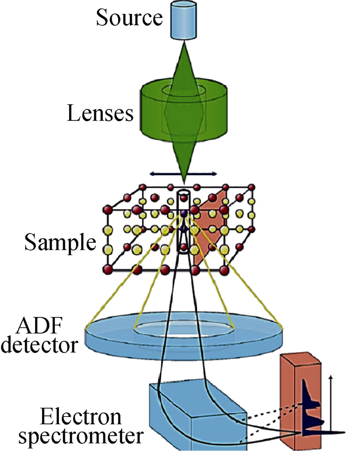
Fig. 1 Schematic diagram for the formation of STEM image[6]
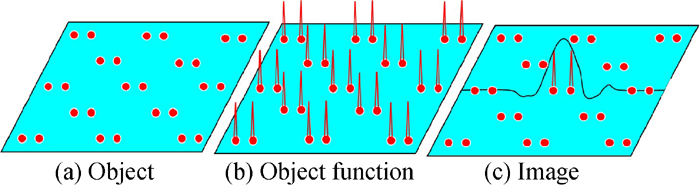
Fig. 2 Potential for high-angle scattering of Si atomic columms The specimen in (a) consists of an array of atomic columns (〈110〉 Si for example), in which the potential for high-angle scattering can be represented by an object function consisting of weighted spikes, as shown in (b). The experimental image can be interpreted as a convolution of the experimental probe and the object function, as in (c)[8]
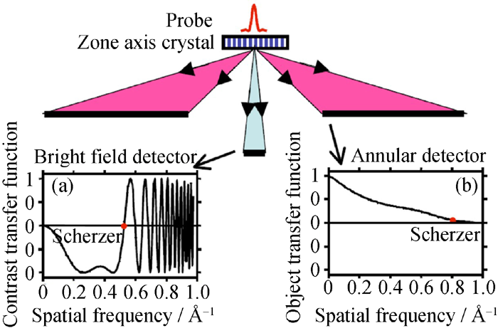
Fig. 3 Different contrast transfer functions of a STEM (VG Microscopes HB501UX STEM operated at 100 kV with a probe size of ~ 0.22 nm) measured simultaneously at (a) coherent and (b) incoherent imaging conditions by using a small bright field detector and a large annular detector, respectively Plots show the very different transfer functions for the two detectors, the bright field detector showing contrast reversals and oscillations characteristic of coherent phase contrast imaging, the dark field detector showing a monotonic decrease in transfer with spatial frequency characteristic of incoherent imaging[6]
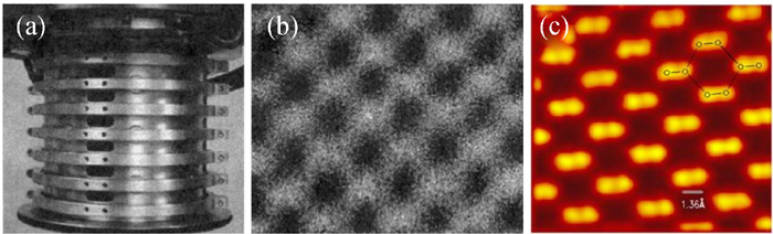
Fig. 4 Aberration corrector and improvement of Z-STEM image resolution [11] (a) An Aberration corrector consisting of 60 optical components, (b) experimental Z-STEM image of Si in [110] orientation taken from VG STEM HB501 STEM with a point resolution of ~ 0.2 nm, un-resolving the dumbbell structure of silicon, and (c) Z-STEM image of Si in [110] orientation taken from VG STEM HB501 STEM equipped with Nion aberration corrector, resolving clearly the dumbbell unit structure of silicon with a point resolution of 0.13 nm and increasing the ratio of signal-to-noise
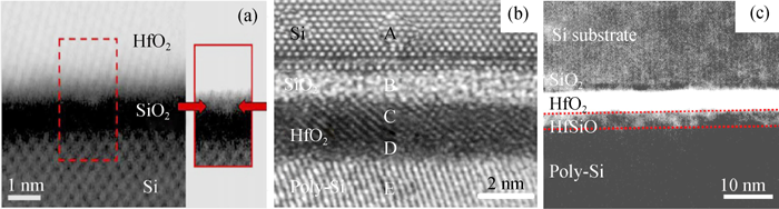
Fig. 5 Images of Si/HfO2 (a) and HfO2/HfSiO (b,c) gate stacks (a) Cross-sectional Z-STEM image of an Si/HfO2 gate stack. The SiO2/HfO2 interface is seen in the center of the image[16]; (b) Cross-sectional HRTEM image of a HfO2/HfSiO gate stack viewed from the [110] direction of Si substrate, and (c) HAADF image of the same stack[17]
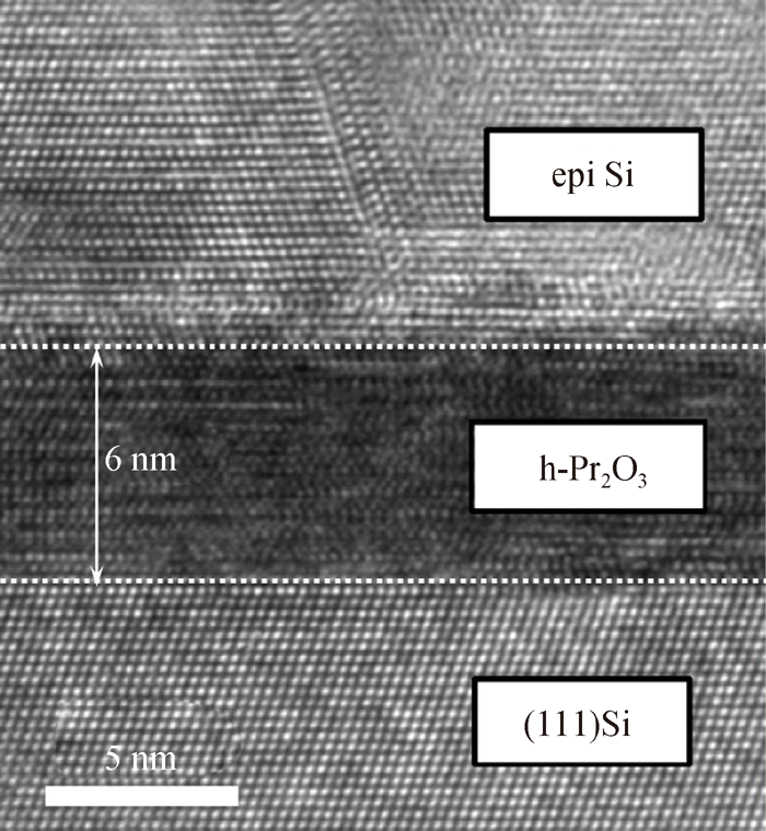
Fig. 6 Cross-sectional HRTEM image of the epitaxial Pr2O3 film (6 nm thick) grown on Si(111) substrate, and the film can be overgrown epitaxially with high quality Si (111) film[20]
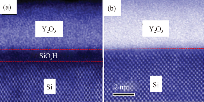
Fig. 7 Z-STEM image of a-Si/Y2O3/c-Si stack (a) The formation of SiOxHy interfacial layer was due to the exposure of Y2O3 film to atmospheric conditions; (b) The interfacial layer of SiOxHy was not visible due to the Y2O3 film in-situ capped by a layer of amorphous Si during the deposited process[21]
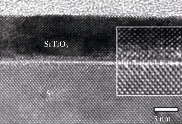
Fig. 8 Cross-sectional HRTEM image of a SrTiO3 film epitaxially grown on Si (100) substrate by MBE, showing the formation of an atomically abrupt crystalline interface between the SrTiO3 and Si[23]
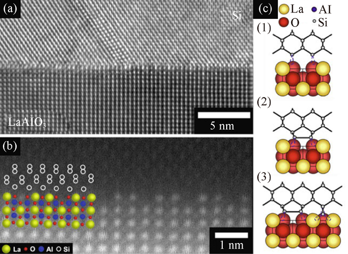
Fig. 9 (a) HRTEM and (b) HAADF-STEM images from an epitaxial Si/LaAlO3 interface showing an interface reconstruction where every third La column is missing at the interface. (c) Interface models based on the HAADF-STEM images[25]
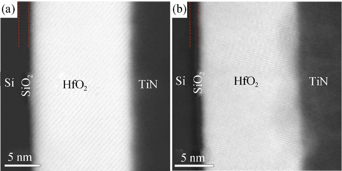
Fig. 10 Z-STEM images of the HfO2 gate dielectrics grown by atomic layer deposition on Si substrates and their interfaces with TiN electrodes and silicon, annealed at (a) 800℃ and (b) 900℃[26] The dashed lines are a guide to the eye to indicate the approximate position of the interfacial layer. Note the roughening of interfaces after annealing at 900℃
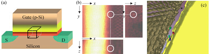
Fig. 11 Three-dimensional locations of single Hf atoms in a Si/SiO2/HfO2 stacked device[30] (a) A schematic view diagram of the Si/SiO2/HfO2 stacked device with a SiO2 layer shown in red and the alternative dielectric, HfO2 shown in yellow color, where S and D representing the source and drain, respectively. (b) Three ADF images of the stack is represented by slice views in planes of x-y, x-z, and y-z, respectively. One isolated single Hf atom is marked the white circles. This representation demonstrates that the Hf atom is located inside the TEM sample. (c) A 3D reconstruction of part of the HfO2/SiO2/Si interface structure showing single Hf atoms. The Si substrate was color coded in gold, whereas the HfO2 film is marked solid yellow. Single Hf atoms with different positions within the interface layer are coded separately in green, black, red, and blue colors, respectively
| [1] | LI D X.High-resolution transmission electron microscopy in materials science-developed history, current status and prospect. J. Chin. Electr. Microscopy Soc., 2000, 19(2): 81-83. |
| [2] | VARELA M, LUPINI A R, BENTHEM K V, et al.Materials characterization in the aberration-corrected scanning transmission electron microscope. Annu. Rev. Mater. Res., 2005, 35: 539-569. |
| [3] | WILK G D, WALLACE R M, ANTHONY J M.High-k gate dielectrics: current status and materials properties considerations. J. Appl. Phys., 2001, 89(10): 5243-5275. |
| [4] | ZHU X H, ZHU J M, LI A D, et al.Challenges in atomic-scale characterization of high-k dielectrics and metal gate electrodes for advanced CMOS gate stacks. J. Mater. Sci. Technol., 2009, 25(3): 289-313. |
| [5] | DELLBY N, KIRVANEK O L, NELLIST P D, et al.Progress in aberration-corrected scanning transmission electron microscopy. J. Electron Microscopy, 2001, 50(3): 177-185. |
| [6] | PENNUCOOK S J.Structure determination through Z-contrast microscopy. Advances in Imaging and Electron Physics, 2002, 123: 173-206. |
| [7] | PENNUCOOK S J, BOATNER L A.Chemically sensitive structure- imaging with a scanning transmission electron microscope. Nature, 1988, 336: 565-567. |
| [8] | BROWNING N D, WALLIS D J, NELLIST P D.EELS in the STEM: determination of materials properties on the atomic scale. Micron, 1997, 28(5): 333-348. |
| [9] | BROWNING N D, BUBAN J P, PROUTEAU C, et al.Investigating the atomic scale structure and chemistry of grain boundaries in High-Tc superconductors. Micron, 1999, 30(3): 425-436. |
| [10] | PENNUCOOK S J, JESSON D E.High-resolution Z-contrast imaging of crystals. Ultramicroscopy, 1991, 37(124):14-38. |
| [11] | PENNUCOOK S J, RAFFERTY B, NELLIST P D.Z-contrast imaging in and aberration-corrected scanning transmission electr on microscope. Microscopy and Microanalysis, 2000, 6: 343-352. |
| [12] | BUCHANAN D.Scaling the gate dielectric: materials, integration, and reliability. IBM J. Res. & Dev., 1999, 43(3): 245-264. |
| [13] | BERSUKER G, ZEITZOFF P, BROWN G, et al.Dielectrics for future transistors. Material Today, 2004, 7(1): 26-33. |
| [14] | ROBERSON J.High dielectric constant gate oxides for metal oxide Si transistors. Rep. Prog. Phys., 2006, 69(2): 327-396. |
| [15] | ZHU X H, ZHU J M, LIU Z G, et al.Characterization of high-K gate dielectrics by atomic-resolution electron microscopy: current progress and future prospects. J. Chin. Electr. Microscopy Soc.,2009, 28(3): 280-302. |
| [16] | GARFUNKELD E, GUSTAFSSON T, LYSAGHT P, et al.Structure, composition and order at interfaces of crystalline oxides and other high-K materials on silicon. FUTURE FAB Inter, 2006, 220: 349-360 |
| [17] | CRAVEN A J, MACKENZIE M, MCCOMB D W, et al. Investigating physical and chemical changes in high-K gate stacks using nanoanalytical electron microscopy. Microelectron Eng., 2005, 80: 90-97. |
| [18] | OSTEN H J, LAHA A, CZERNOHORSKY M, et al.Introducing crystalline rare-earth oxides into Si technologies. Phys. Stat. Sol.(a), 2008, 205(4): 695-707 . |
| [19] | LAHA A, FISSEL A, BUGIEL E, et al.Epitaxial multi-component rare earth oxide for high-K application. Thin Solid Films, 2007, 515(16): 6512-6517. |
| [20] | OSTEN H J, CZERNOHORSKY M, DARGIS R, et al.Integration of functional epitaxial oxides into silicon: from high-K application to nanostructures. Microelectron Eng., 2007, 84(9/10): 2222-2225. |
| [21] | BUSCH B W, PLUCHERY O, CHABAL Y J, et al.Materials characterization of alternative gate dielectrics. MRS Bull., 2002, 27(3): 206-211. |
| [22] | SCHLOM D G, HAENI J H.A thermodynamic approach to selecting alternative gate dielectrics. MRS Bull., 2002, 27(3): 198-204 . |
| [23] | MARCHIORI C, SOUSA M, GUILLER A, et al. Thermal stability of the SrTiO3/(Ba,Sr)O3 stacks epitaxially grown on Si. Appl. Phys. Lett., 2006, 88(7): 072913-1-3. |
| [24] | NORGA G J, MARCHIORI C, ROSSEL C, et al. Solid phase epitaxy of SrTiO3 on (Ba,Sr)O/Si(100): the relationship between oxygen stoichiometry and interface stability. J. Appl. Phys., 2006, 99(8): 84102-1-7. |
| [25] | KLENOV D O, SCHLOM D G, Li H, et al. The interface between single crystalline (001) LaAlO3 and (001) silicon. Jpn. J. Appl. Phys., 2005, 44(20-23): L617-L619. |
| [26] | AGUSTIN M P, FONSECA L R C, HOOKER J C, et al. Scanning transmission electron microscopy of gate stacks with HfO2 dielectrics and TiN electrodes. Appl. Phys. Lett., 2005, 87(12): 121909-1-3. |
| [27] | CHOI K, ALSHAREEF H N, WEN H C, et al. Effective work function modification of atomic-layer-deposited-TaN film by capping layer. Appl. Phys. Lett., 2006, 89(3): 032113-1-3. |
| [28] | ANDERSON S C, BIRKELAND C R, ANSTIS G R, et al.An approach to quantitative compositional profiling at near-atomic resolution using high-angle annular dark field imaging. Ultramicroscopy, 1997, 69(2): 83-103. |
| [29] | PENNUCOOK S J, JESSON D E, MCGIBBON A J, et al.High angle dark field STEM for advanced materials. J. Electron Microscopy, 1996, 45(1): 36-43. |
| [30] | BENTHEMA K V, LUPINI A R, KIM M Y, et al. Three-dimensional imaging of individual hafnium atoms inside a semiconductor device. Appl. Phys. Lett., 2005, 87(3): 034104-1-3. |
| [1] | CHEN Mingjun, MIAO Hongkang, XIAO Yingjun, DENG Jianbo, ZHANG Xiang, ZHAO Jiupeng, LI Yao. Photo- and Thermo-chromic Dual-responsive Materials: A Review on Design Strategies and Applications in Smart Windows [J]. Journal of Inorganic Materials, 2026, 41(6): 723-738. |
| [2] | SONG Kunjie, XIE Rongjun. Research Advances on Machine Learning-driven Development of Novel Luminescent Materials [J]. Journal of Inorganic Materials, 2026, 41(6): 689-703. |
| [3] | HU Yuqing, ZHU Yixin, LE Xianhao, WAN Qing. Lithium Tantalate Wafer: Advances in Thinning Technology and Application in Pyroelectric Infrared Detectors [J]. Journal of Inorganic Materials, 2026, 41(6): 764-774. |
| [4] | LIU Chunfan, CHEN Ke, GE Fangfang, HUANG Qing. Research Progress on Lead-bismuth Eutectic Corrosion Resistant Coatings [J]. Journal of Inorganic Materials, 2026, 41(6): 775-786. |
| [5] | HU Yang, XIE Min, ZHANG Xiaoyi, LI Xiang, GUO Xinwei, JIANG Nan, ZHOU Wenhan, ZHANG Shengli, ZENG Haibo. Research Progress on Computational and Data-driven Environmental-friendly Luminescent Materials [J]. Journal of Inorganic Materials, 2026, 41(6): 704-722. |
| [6] | WANG Junbu, HUANG Zeai, YANG Mingkai, MENG Ying, ZHOU Mingwei, ZHOU Ying. Research Progress on Anti-coking Catalytic Materials for Methane Conversion [J]. Journal of Inorganic Materials, 2026, 41(6): 739-750. |
| [7] | WANG Jinwen, YANG Zhen, ZHOU Huan, XIA Dan, YANG Lei. Biomedical Applications of Injectable Inorganic Biomaterials [J]. Journal of Inorganic Materials, 2026, 41(6): 751-763. |
| [8] | LI Hantao, SHEN Qiang, LUO Guoqiang, WANG Xuefei, GAO Ming, CHEN Chen. Research Progress on Structure and Performance Regulation of Silicon-based Anode Materials via Mechanical Ball Milling [J]. Journal of Inorganic Materials, 2026, 41(5): 561-572. |
| [9] | XIE Chenyi, MIAO Huaming, ZHANG Weiran, LIU Rongjun, WANG Yanfei, LI Duan. Research Progress on Theoretical Calculation in the Field of High-entropy Ceramics [J]. Journal of Inorganic Materials, 2026, 41(5): 545-560. |
| [10] | LI Xuan, YE Kuicai, FENG Jiayin, QIU Jiajun, QIAN Wenhao, XING Min. Surface Modification of Titanium-based Dental Implants for Soft Tissue Sealing: A Review [J]. Journal of Inorganic Materials, 2026, 41(4): 432-444. |
| [11] | PENG Dezhao, LI Rui, WANG Wenhong, WANG Zirui, ZHANG Zhizhen. Research Progress on Sodium Chloride Solid Electrolytes [J]. Journal of Inorganic Materials, 2026, 41(4): 409-420. |
| [12] | CHEN Kun, JIANG Yonggang, FENG Junzong, LI Liangjun, HU Yijie, FENG Jian. Research Progress on Lanthanum Zirconate Porous Materials for Thermal Insulation [J]. Journal of Inorganic Materials, 2026, 41(4): 421-431. |
| [13] | WEI Lianjin, QI Zhijie, WANG Xin, ZHU Junwu, FU Yongsheng. Modification of Nanodiamond and Its Application in Electrocatalytic Oxygen Reduction Reaction [J]. Journal of Inorganic Materials, 2026, 41(3): 273-288. |
| [14] | LIU Zhanyi, LI Mian, OUYANG Xiaoping, CHAI Zhifang, HUANG Qing. Recent Progress on Removal of Sr/Cs from Molten Salt in Dry Reprocessing [J]. Journal of Inorganic Materials, 2026, 41(2): 150-158. |
| [15] | SUN Lian, ZHANG Leilei, XUE Zexu, WU Kun, CHEN Ye, LI Zhiyuan, WANG Lukai, WANG Zungang. Research Progress on Zero-dimensional Metal Halide Scintillators towards Radiation Detection Applications [J]. Journal of Inorganic Materials, 2026, 41(2): 159-176. |
| Viewed | ||||||
|
Full text |
|
|||||
|
Abstract |
|
|||||