无机材料学报 ›› 2019, Vol. 34 ›› Issue (7): 748-754.DOI: 10.15541/jim20180443 CSTR: 32189.14.10.15541/jim20180443
郭钰1,2,彭同华1,2( ),刘春俊1,杨占伟1,蔡振立1
收稿日期:2018-09-20
修回日期:2018-11-13
出版日期:2019-07-20
网络出版日期:2019-06-26
作者简介:郭 钰(1983-), 女, 副研究员. E-mail:guoyu03201@sina.com
基金资助:
GUO Yu1,2,PENG Tong-Hua1,2(),LIU Chun-Jun1,YANG Zhan-Wei1,CAI Zhen-Li1
Received:2018-09-20
Revised:2018-11-13
Published:2019-07-20
Online:2019-06-26
Supported by:摘要:
本研究探讨了同质外延生长的4H-SiC晶片表面堆垛层错(SF)的形貌特征和起因。依据表面缺陷检测设备KLA-Tencor CS920的光致发光(PL)通道和形貌通道的特点, 将SF分为五类。其中I类SF在PL通道图中显示为梯形, 在形貌图中不显示; II类SF在PL通道图中显示为三角形, 且与I类SF重合, 在形貌图中显示为胡萝卜形貌。III-V类SF在PL通道图中均显示为三角形, 在形貌图中分别显示为胡萝卜、无对应图像或三角形。研究结果表明, I类SF起源于衬底的基平面位错(BPD)连线, 该连线平行于<1$\bar{1}$00>方向, 在生长过程中沿着<11$\bar{2}$0>方向移动, 形成基平面SF。II类和大部分的III-IV类SF起源于衬底的BPD, 其中一个BPD在外延过程中首先转化为刃位错(TED), 并在外延过程中延<0001>轴传播, 其余BPD或由TED分解形成的不全位错(PDs)在(0001)面内传播形成三角形基平面SF。其余的III-V类SF起源于衬底的TED或其它。II-III类SF在形貌通道中显示为胡萝卜, 而IV类SF不显示, 主要区别在于外延过程中是否有垂直于(0001)面的棱镜面SF与表面相交。上述研究说明减少衬底的BPD, 对减少外延层中的SF尤为重要。
中图分类号:
郭钰, 彭同华, 刘春俊, 杨占伟, 蔡振立. 4H-SiC外延层中堆垛层错与衬底缺陷的关联性研究[J]. 无机材料学报, 2019, 34(7): 748-754.
GUO Yu, PENG Tong-Hua, LIU Chun-Jun, YANG Zhan-Wei, CAI Zhen-Li. Correlation between Stacking Faults in Epitaxial Layers of 4H-SiC and Defects in 4H-SiC Substrate[J]. Journal of Inorganic Materials, 2019, 34(7): 748-754.
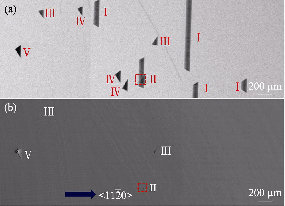
图1 CS920检测SF的图像(a)激发波长为355nm的PL通道图和(b)形貌通道图
Fig. 1 SF images tested by CS920 (a) PL images excited by 355 nm wavelength; (b) morphology images
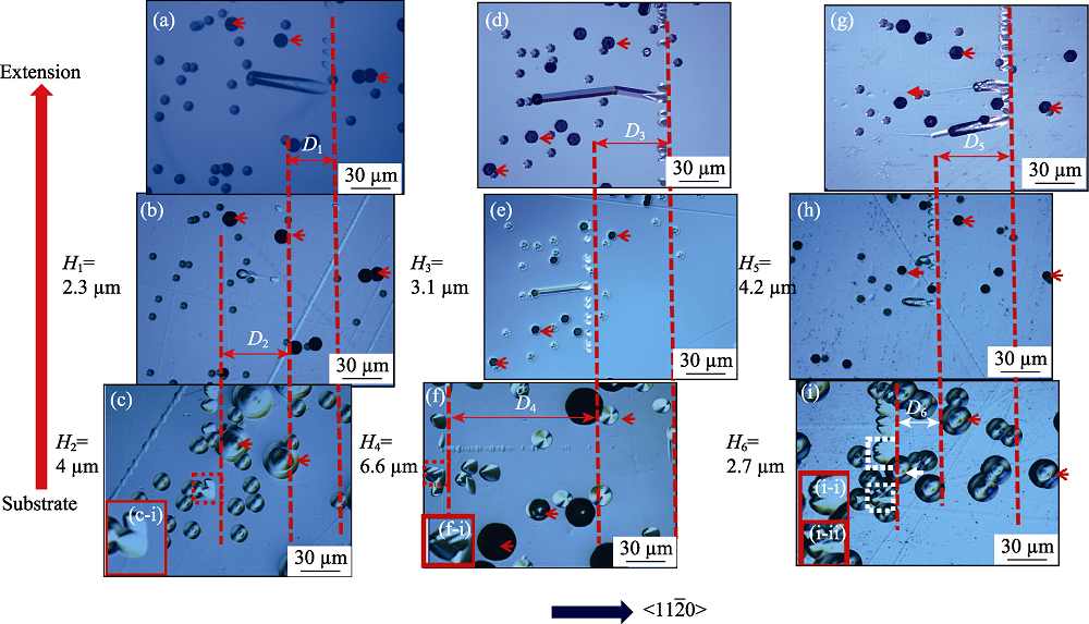
图2 I类和II类SF的起因和繁衍特征, <11$\bar{2}$0>方向是晶体生长的下台阶方向, D1~D6标记平行条纹的移动距离, H1~H6标记外延层的去除厚度
Fig. 2 Originations and propagations of SF I and SF II<11$\bar{2}$0> is the direction of lower steps of crystal growth. D1-D6 are the moving distances of BPD lines. H1-H6 are the removing thickness of epitaxial layers
| No. | 1 | 2 | 3 | 4 | 5 | 6 |
|---|---|---|---|---|---|---|
| Moving distance of BPD lines, D/μm | 33 | 57 | 44 | 94 | 60 | 39 |
| Removing thickness, H/μm | 2.3 | 4 | 3.1 | 6.6 | 4.2 | 2.7 |
表1 图2中平行条纹移动的距离D和外延层去除厚度H的对应关系
Table 1 Relationship of moving distance D of BPD lines and removing thickness H of epitaxial layers in Fig. 2
| No. | 1 | 2 | 3 | 4 | 5 | 6 |
|---|---|---|---|---|---|---|
| Moving distance of BPD lines, D/μm | 33 | 57 | 44 | 94 | 60 | 39 |
| Removing thickness, H/μm | 2.3 | 4 | 3.1 | 6.6 | 4.2 | 2.7 |
| Test position | Substrate | Epitaxial layers |
|---|---|---|
| N concentration | 8×10¹² | <1010 |
表2 二次离子质谱(SIMS)检测衬底和外延层中的N含量
Table 2 Nitrogen concentration in substrate and epitaxial layers tested by SIMS
| Test position | Substrate | Epitaxial layers |
|---|---|---|
| N concentration | 8×10¹² | <1010 |
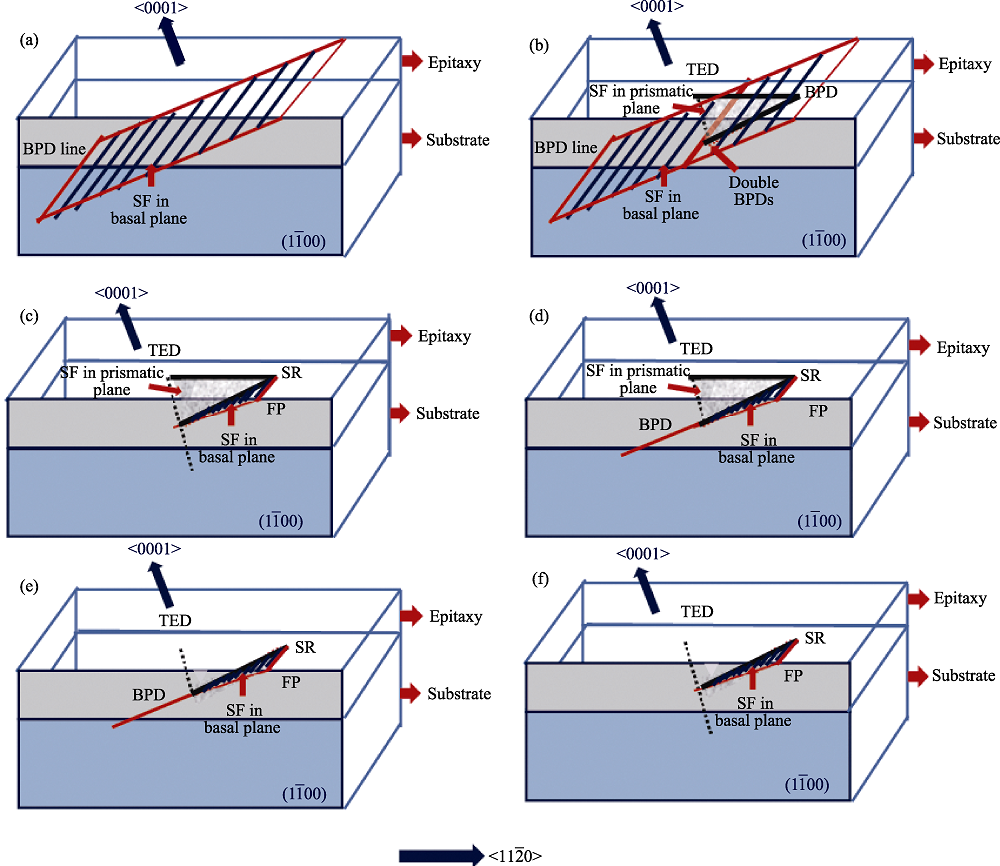
图3 (a) SF I; (b) SF II; (c)~(d) SF III; (e)~(f) SF IV的繁衍规律示意图
Fig. 3 Propagation diagrams of (a) SF I, (b) SF II, (c)-(d) SF III, and (e)-(f) SF IV
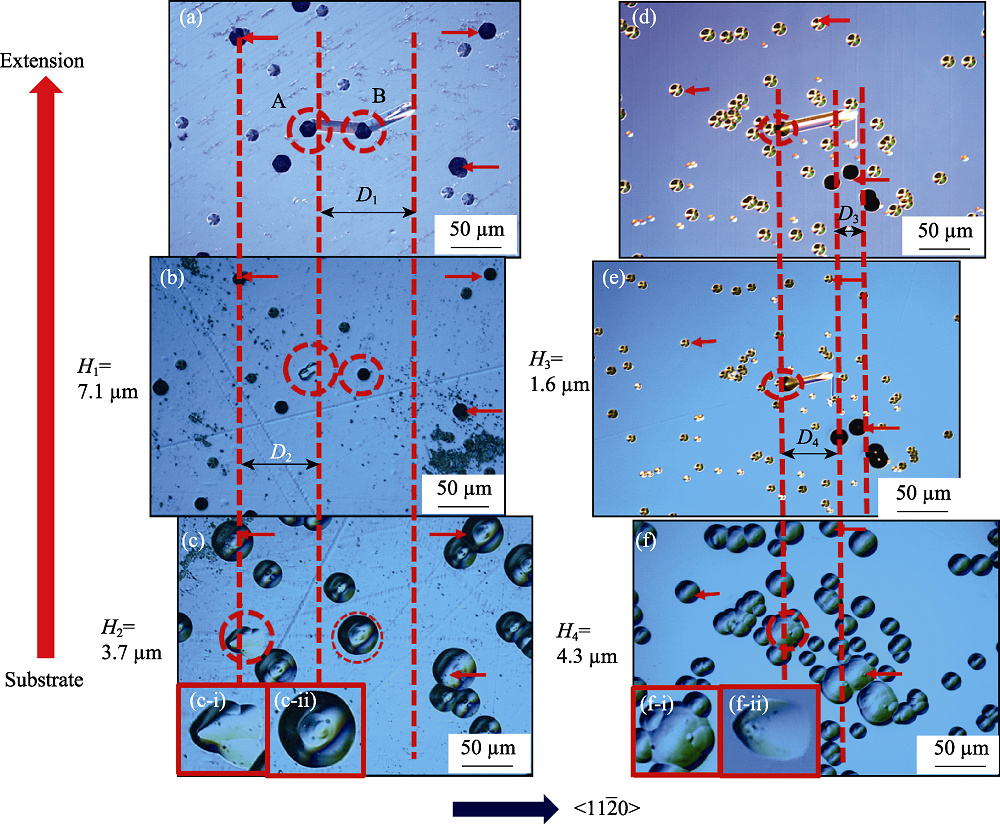
图4 III类SF的起因和繁衍特征, <11$\bar{2}$0>方向是晶体生长的下台阶方向, D1~D4标记胡萝卜尾部的移动距离, H1~H4标记外延层的去除厚度
Fig. 4 Originations and propagations of SF III<11$\bar{2}$0> is the direction of lower steps of crystal growth. D1-D4 are the moving distances of BPD lines. H1-H4 are the removing thickness of epitaxial layers
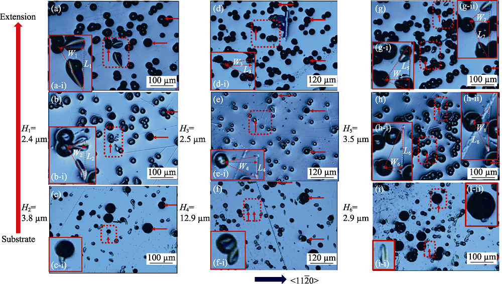
图5 IV类SF起因和繁衍特征, <11$\bar{2}$0>方向是晶体生长的下台阶方向, H1~H6标记外延层的去除厚度, L1~L8是三角形底边长度, W1~W8是三角形顶点到底边的垂直距离
Fig. 5 Originations and propagations of SF IV<11$\bar{2}$0> is the direction of lower steps of crystal growth. H1~H6 are the removing thickness of epitaxial layers. L1~L8 are bottom lengths of triangle defects. W1~W8 are widths of triangle defects
| No. | 1 | 2 | 3 | 4 |
|---|---|---|---|---|
| Moving distance of BPD lines, D/μm | 102 | 53 | 23 | 61 |
| Removing thickness, H/μm | 7.1 | 3.7 | 1.6 | 4.3 |
表3 图3中平行条纹移动的距离D和外延层去除厚度H的对应关系
Table 3 Relationship of the moving distance D of BPD lines and the removing thickness H of epitaxial layers in Fig. 3
| No. | 1 | 2 | 3 | 4 |
|---|---|---|---|---|
| Moving distance of BPD lines, D/μm | 102 | 53 | 23 | 61 |
| Removing thickness, H/μm | 7.1 | 3.7 | 1.6 | 4.3 |
| No. | 1 | 2 | 3 | 4 | 5 | 6 | 7 | 8 |
|---|---|---|---|---|---|---|---|---|
| Moving distance of BPD lines, D/μm | 34 | - | 36 | - | 50 | - | - | - |
| Removing thickness, H/μm | 2.4 | 3.8 | 2.5 | 12.9 | 3.5 | 2.9 | - | - |
| With triangle defects, W/μm | 85 | 51 | 85 | 49.0 | 85 | 35 | 85 | 35 |
| Bottom lengths of triangle defects, L/μm | 105 | 63 | 90 | 52 | 60 | 25 | 110 | 45 |
表4 图5中平行条纹移动的距离D、外延层去除厚度H、三角形缺陷宽度W和底边长度L的对应关系表
Table 4 Relationship of the moving distance D of BPD lines, the removing thickness H of epitaxial layers and width of trianagle defects W with bottom lengths of triangle defects in Fig. 3
| No. | 1 | 2 | 3 | 4 | 5 | 6 | 7 | 8 |
|---|---|---|---|---|---|---|---|---|
| Moving distance of BPD lines, D/μm | 34 | - | 36 | - | 50 | - | - | - |
| Removing thickness, H/μm | 2.4 | 3.8 | 2.5 | 12.9 | 3.5 | 2.9 | - | - |
| With triangle defects, W/μm | 85 | 51 | 85 | 49.0 | 85 | 35 | 85 | 35 |
| Bottom lengths of triangle defects, L/μm | 105 | 63 | 90 | 52 | 60 | 25 | 110 | 45 |
| [1] | PENG T H, LIU C J, WANG B , et al. Progress in growth and physical properties of wide band gap semiconductor silicon carbide single crystals. Journal of Synthetic Crystal, 2012,S1:234-241. |
| [2] |
PENG T H, YANG H, JIAN J K , et al. Factors affecting the formation of misoriented domains in 6H-SiC single crystals grown by PVT method.[J]. Cryst. Res. Technol., 2009,44(4):357-362.
DOI URL |
| [3] | CHANG S H, LIU X C, HUANG W , et al. Preparation and properties of lateral contact structure SiC photoconductive semiconductor switches. Journal of Inorganic Materials, 2012,27(10):1058-1062. |
| [4] |
WANG B, PENG T H, LIANG J K , et al. Characterizations and formation mechanism of a new type of defect related to nitrogen doping in SiC crystals. Appl. Phys.A, 2014,117(3):1563-1569.
DOI URL |
| [5] |
LIU C J, CHEN X L, PENG T H , et al. Step flow and polytype transformation in growth of 4H-SiC crystals. J. Cryst. Growth, 2014,394:126-131.
DOI URL |
| [6] |
SUN W, SONG Y T, LIU C J , et al. Basal plane dislocation- threading edge dislocation complex dislocations in 6H-SiC single crystals. Mater.Express, 2015,5(1):63-67.
DOI URL |
| [7] |
LIU C J, PENG T H, WANG S C , et al. Formation mechanism of type 2 micropipe defects in 4H-SiC crystals. CrystEngComm, 2013,15(7):1307-1313.
DOI URL |
| [8] |
ZHAO N, LIU C J, WANG B , et al. Stacking faults in 4H-SiC single crystal. Journal of Inorganic Materials, 2018,33(5):540-544.
DOI URL |
| [9] |
LIU K X, STAHLBUSH R E, TWIGG M E , et al. Photoluminescence and electroluminescence imaging of carrot defect in 4H-SiC epitaxy. Journal of Electronic Materials, 2007,36(4):297-306.
DOI URL |
| [10] | ZHANG X, HA S Y, BENAMARA S , et al. Structure of carrot defects in 4H-SiC epilayers. Materials Science Forum, 2006, 527-529:327-332. |
| [11] |
MIAO M S, WALTER R L . Stacking faults and 3C quantum wells in hexagonal SiC polytypes. Mater.Sci.Forum, 2006, 527-529:351-354.
DOI URL |
| [12] |
WANG Y, CHERT L, MILDAOV M K , et al. Characterization of stacking fault induced behavior in 4H-SiC p-i-n diodes.Mater. Sci.Forum, 2006, 527-529:363-366.
DOI URL |
| [13] |
HIDEYUKI U, KEISUKE F, MASANHIKO I , et al. Analysis and reduction of stacking faults in fast epitaxial growth. Materials Science Forum, 2016 858:173-176.
DOI URL |
| [14] | RADU H, STEFAN G S, DENIS E T , et al. Identification of stacking faults in silicon carbide by polarization-resolved second harmonic generation microscopy. Scientific Reports, 2017, 7(1): 4870-1-9. |
| [15] | HIDEKAZU Y . Assessment of stacking faults in silicon carbide crystals. Sensors and Materials, 2013,25(3):177-187. |
| [16] |
HASSAN J, HENRY A, IVANOV I G , et al. In-grown stacking faults in 4H-SiC epilayers grown on off-cut substrates. Journal of Applied Physics, 2009,105(12):123513.
DOI URL |
| [17] |
ZHOU R W, LIU X C, GUO H J , et al. Study of triangle-shaped defects on nearly on-axis 4H-SiC substrates. Materials Science Forum, 2016,858:225-228.
DOI URL |
| [18] |
HASSAN J, BERGMAN J P . Single Shockley stacking faults in as-grown 4H-SiC epilayers. Materials Science Forum, 2010, 645-648:327-330.
DOI URL |
| [19] |
LIJIMA A, KAMATA I , TSUCHIDA, H, et al. Correlation between shapes of Shockley stacking faults and structures of basal plane dislocations in 4H-SiC epilayers. Philosophical Magazine, 2017,97(30):2736-2752.
DOI URL |
| [20] |
STAHLBUSH R E, MYERS-WARD R L, VANMIL B L , et al. A pictorial tracking of basal plane dislocations in SiC epitaxy. Materials Science Forum, 2010, 645-648:271-276.
DOI URL |
| [21] | OKOJIE R S, HUANG X, DUDLEY M , et al. Process-induced deformations and stacking faults in 4H-SiC. MRS Proceedings, 2011,911:B07-02. |
| [22] |
LIU K X, STAHLBUSH R E, TWIGG M E , et al. Photoluminescence and electroluminescence imaging of carrot defect in 4H-SiC epitaxy. Journal of Electronic Materials, 2007,36(4):297-306.
DOI URL |
| [23] | YUTARO M, SHUHEI Y, YASUTO H , et al. Photoluminescence study of oxidation-induced stacking faults in 4H-SiC epilayers. Materials Science Forum Vols., 2015,5(12):327-330. |
| [24] | LI Z Y, LIU L T, DONG X , et al. Defects in homogeneous epitaxial layers of 4H-SiC. Equipment for Electronic Products Manufacturing, 2005,11(130):62-64. |
| [25] |
MIAO M S, WALTER R L . Stacking faults and 3C quantum wells in hexagonal SiC polytypes. Mater. Sci. Forum, 2006, 527-529:351-354.
DOI URL |
| [26] |
KATSUNO M, NAKABAYASHI M, FUJIMOTO T , et al. Stacking fault formation in highly nitrogen-doped 4H-SiC substrates with different surface preparation conditions. Mater.Sci.Forum, 2008, 600-603:341-344.
DOI URL |
| [27] |
KUHR T A, LIU J Q, CHUNG H J , et al. Spontaneous formation of stacking faults in highly doped 4H-SiC during annealing.[J]. Appl. Phys., 2002,92(10):5863-5871.
DOI URL |
| [28] | GALECKAS A, LINNROS J, PIROUZ P , et al. Recombination- induced stacking faults: evidence for a general mechanism in hexagonal SiC. Phys. Rev. Lett., 2006, 96(2): 025502-1-4. |
| [29] |
OHNO T, YAMAGUCHI H, KURODA S , et al. Direct observation of dislocations propagated from 4H-SiC substrate to epitaxial layer by X-ray topograghy. Joumal of Crystal Growth, 2004,260:209-216.
DOI URL |
| [30] |
HASSAN J, HENRY A, MCNALLY P J , et al. Characterization of the carrot defect in 4H-SiC epitaxial layers. Journal of Crystal Growth, 2010,312(11):1828-1837.
DOI URL |
| [1] | 刘雷敏, 罗红心, 何玉梅, 金利民, 李永杰, 刘静雯, 魏玉全, 孙安乐, 陈忠明, 刘学建, 殷杰, 黄政仁. 先进光源装置用碳化硅反射镜性能研究[J]. 无机材料学报, 2026, 41(6): 805-813. |
| [2] | 蒋圣楠, 郑重, 何唯一, 刘涛, 潘秀红, 陈锟, 郭辉, 高攀, 刘春俊, 刘学超. 硼镓共掺氧化锌透明电极的制备及性能优化[J]. 无机材料学报, 2026, 41(4): 479-485. |
| [3] | 徐浩, 顾海涛, 吴鸿辉, 岳晓飞, 林思琪, 金敏. Bi掺杂InSe晶体生长及性能研究[J]. 无机材料学报, 2026, 41(4): 493-499. |
| [4] | 曹娟, 吴西士, 刘泽华, 裴兵兵, 韩建燊, 刘欢, 杨亦天, 吴海波, 黄政仁. 晶粒尺寸对常压固相烧结SiC陶瓷断裂强度Weibull分布的影响[J]. 无机材料学报, 2026, 41(2): 217-224. |
| [5] | 王鲁杰, 张玉新, 李彤阳, 于源, 任鹏伟, 王建章, 汤华国, 姚秀敏, 黄毅华, 刘学建, 乔竹辉. 深海服役环境下碳化硅陶瓷材料的腐蚀及磨损行为[J]. 无机材料学报, 2025, 40(7): 799-807. |
| [6] | 李紫薇, 弓伟露, 崔海峰, 叶丽, 韩伟健, 赵彤. 前驱体法制备(Zr, Hf, Nb, Ta, W)C-SiC复相陶瓷及性能研究[J]. 无机材料学报, 2025, 40(3): 271-280. |
| [7] | 王浩, 刘学超, 郑重, 潘秀红, 徐锦涛, 朱新锋, 陈锟, 邓伟杰, 汤美波, 郭辉, 高攀. 非本征背照触发平面型4H-SiC光导开关性能研究[J]. 无机材料学报, 2024, 39(9): 1070-1076. |
| [8] | 王康龙, 殷杰, 陈晓, 王力, 刘学建, 黄政仁. 颗粒级配对选区激光烧结打印结合常压固相烧结制备碳化硅陶瓷性能的影响[J]. 无机材料学报, 2024, 39(7): 754-760. |
| [9] | 孙川, 何鹏飞, 胡振峰, 王荣, 邢悦, 张志彬, 李竞龙, 万春磊, 梁秀兵. 含有石墨烯阵列的SiC基陶瓷材料的制备与力学性能[J]. 无机材料学报, 2024, 39(3): 267-273. |
| [10] | 徐昊, 钱伟, 花银群, 叶云霞, 戴峰泽, 蔡杰. 皮秒激光加工的微织构对碳化硅润湿性的影响[J]. 无机材料学报, 2023, 38(8): 923-930. |
| [11] | 陈强, 白书欣, 叶益聪. 热管理用高导热碳化硅陶瓷基复合材料研究进展[J]. 无机材料学报, 2023, 38(6): 634-646. |
| [12] | 王华进, 寇华敏, 王墉哲, 姜大朋, 张博, 钱小波, 王静雅, 朱琳玲, 曾爱军, 杨秋红, 苏良碧. 193 nm激光下不同含量Y杂质CaF2晶体辐照损伤研究[J]. 无机材料学报, 2023, 38(2): 219-224. |
| [13] | 顾薛苏, 殷杰, 王康龙, 崔崇, 梅辉, 陈忠明, 刘学建, 黄政仁. 颗粒级配对黏结剂喷射打印碳化硅陶瓷性能的影响[J]. 无机材料学报, 2023, 38(12): 1373-1378. |
| [14] | 熊希希, 杨祥龙, 陈秀芳, 李晓蒙, 谢雪健, 胡国杰, 彭燕, 于国建, 胡小波, 王垚浩, 徐现刚. 低位错密度8英寸导电型碳化硅单晶衬底制备[J]. 无机材料学报, 2023, 38(11): 1371-1372. |
| [15] | 吴松泽, 周洋, 李润丰, 刘晓倩, 李翠伟, 黄振莺. 铁尾矿及其反应烧结多孔陶瓷的制备与性能研究[J]. 无机材料学报, 2023, 38(10): 1193-1199. |
| 阅读次数 | ||||||
|
全文 |
|
|||||
|
摘要 |
|
|||||