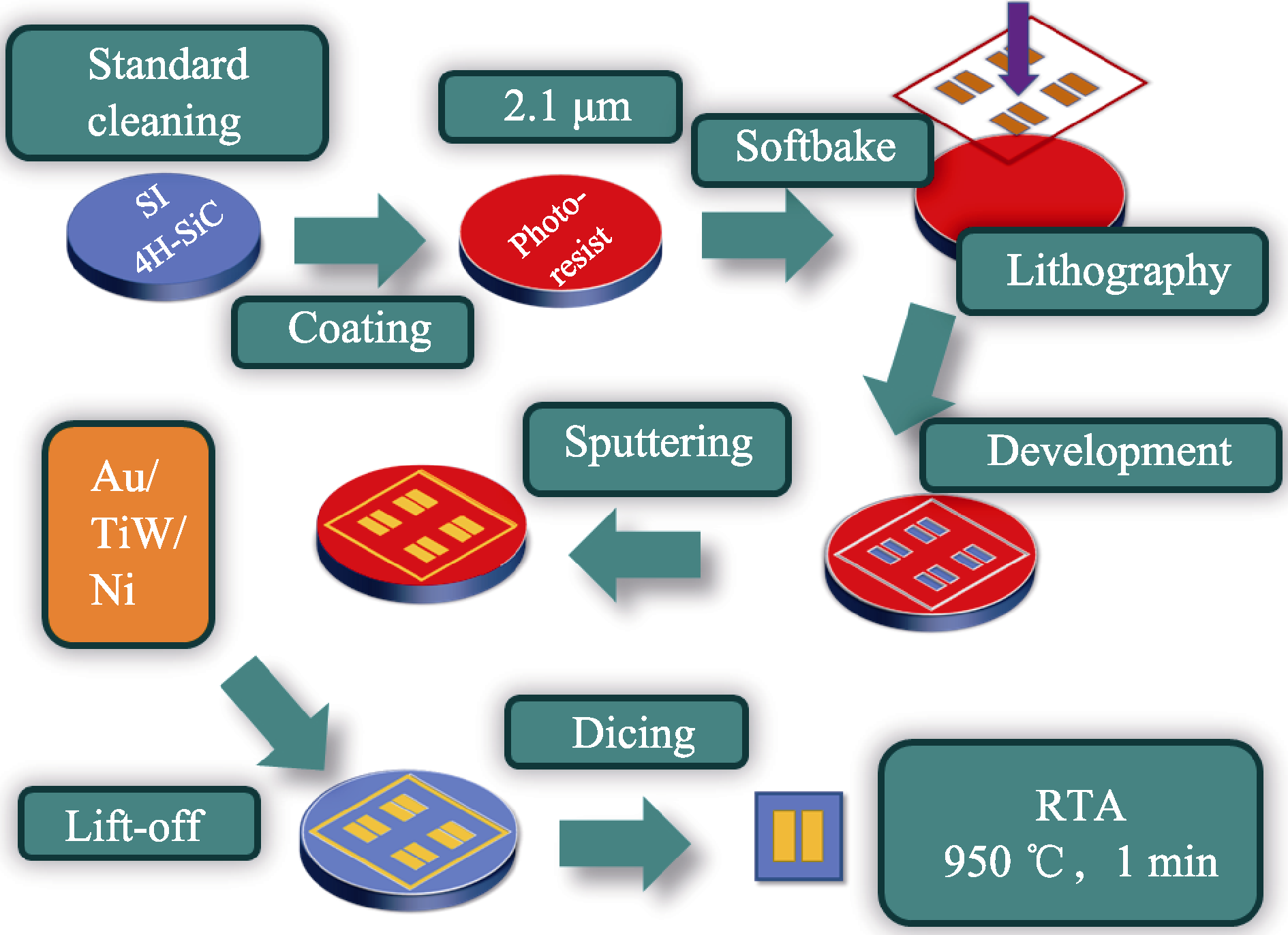
| [1] |
CHANG S H, LIU X C, HUANG W, et al. Preparation and properties of lateral contact structure SiC photoconductive semiconductor switches. Journal of Inorganic Materials, 2012, 27(10): 1058.
|
| [2] |
BRAGG J W, SULLIVAN W W, MAUCH D, et al. All solid-state high power microwave source with high repetition frequency. Review of Scientific Instruments, 2013, 84(5): 054703.
|
| [3] |
HARRIS J R, BLACKFIELD D, CAPORASO G J, et al. Vacuum insulator development for the dielectric wall accelerator. Journal of Applied Physics, 2008, 104(2): 023301.
|
| [4] |
ZHANG D, XU Z, CHENG G, et al. Strongly enhanced THz generation enabled by a graphene hot-carrier fast lane. Nature Communications, 2022, 13: 6404.
DOI
PMID
|
| [5] |
YAN C F, SHI E W, CHEN Z Z, et al. Super fast and high power SiC photoconductive semiconductor switches. Journal of Inorganic Materials, 2008, 23(3): 425.
|
| [6] |
MAJDA-ZDANCEWICZ E, SUPRONIUK M, PAWŁOWSKI M, et al. Current state of photoconductive semiconductor switch engineering. Opto-Electronics Review, 2018, 26(2): 92.
|
| [7] |
CHOWDHURY A R, NESS R, JOSHI R P. Assessing lock-on physics in semi-insulating GaAs and InP photoconductive switches triggered by subbandgap excitation. IEEE Transactions on Electron Devices, 2018, 65(9): 3922.
|
| [8] |
XU M, WANG Y, LIU C, et al. Photoexcited carrier dynamics in a GaAs photoconductive switch under nJ excitation. Plasma Science and Technology, 2022, 24(7): 075503.
|
| [9] |
JAMES C, HETTLER C, DICKENS J. Design and evaluation of a compact silicon carbide photoconductive semiconductor switch. IEEE Transactions on Electron Devices, 2011, 58(2): 508.
|
| [10] |
YANG F, WANG Z, LIANG Z, et al. Electrical performance advancement in SiC power module package design with kelvin drain connection and low parasitic inductance. IEEE Journal of Emerging and Selected Topics in Power Electronics, 2019, 7(1): 84.
|
| [11] |
CHU X, LIU J, XUN T, et al. MHz repetition frequency, hundreds kilowatt, and sub-nanosecond agile pulse generation based on linear 4H-SiC photoconductive semiconductor. IEEE Transactions on Electron Devices, 2022, 69(2): 597.
|
| [12] |
SULLIVAN J S, STANLEY J R. 6H-SiC photoconductive switches triggered at below bandgap wavelengths. IEEE Transactions on Dielectrics and Electrical Insulation, 2007, 14(4): 980.
|
| [13] |
HETTLER C, SULLIVAN W W, DICKENS J, et al. Performance and optimization of a 50 kV silicon carbide photoconductive semiconductor switch for pulsed power applications. Proceedings of the 2012 IEEE International Power Modulator and High Voltage Conference, San Diego, 2012.
|
| [14] |
HUANG J, HU L, MA Z, et al. Study on photoelectric efficiency and failure mechanism of high purity 4H-SiC PCSS. IEEE Transactions on Electron Devices, 2023, 70(11): 5762.
|
| [15] |
ZHU K, DOGAN S, MOON Y T, et al. Effect of n+-GaN subcontact layer on 4H-SiC high-power photoconductive switch. Applied Physics Letters, 2005, 86(26): 261108.
|
| [16] |
XIAO L, YANG X, DUAN P, et al. Effect of electron avalanche break-down on a high-purity semi-insulating 4H-SiC photoconductive semiconductor switch under intrinsic absorption. Applied Optics, 2018, 57(11): 2804.
|
| [17] |
MAUCH D, SULLIVAN W, BULLICK A, et al. High power lateral silicon carbide photoconductive semiconductor switches and investigation of degradation mechanisms. IEEE Transactions on Plasma Science, 2015, 43(6): 2021.
|
| [18] |
ZHENG Z, HUANG W, HAN W W, et al. Analyzing the effects of aluminum-doped ZnO and Ag layers for the transparent electrode vertical PCSS. IEEE Transactions on Electron Devices, 2020, 67(6): 2414.
|
| [19] |
ZHOU T Y, LIU X C, HUANG W, et al. Application of an Al-doped zinc oxide subcontact layer on vanadium-compensated 6H-SiC photoconductive switches. Chinese Physics B, 2015, 24(4): 044209.
|
| [20] |
WANG B, WANG L, NIU X, et al. Breakdown behavior of SiC photoconductive switch with transparent electrode. AIP Advances, 2022, 12(8): 085210.
|
| [21] |
CHOWDHURY A R, MAUCH D, JOSHI R P, et al. Contact extensions over a high-k dielectric layer for surface field mitigation in high power 4H-SiC photoconductive switches. IEEE Transactions on Electron Devices, 2016, 63(8): 1.
|
| [22] |
FENG Z, LUAN C, XIAO L, et al. Performance of a novel rear-triggered 4H-SiC photoconductive semiconductor switch. IEEE Transactions on Electron Devices, 2023, 70(2): 627.
|
| [23] |
FU W, WANG L, WANG B, et al. Investigation on the photocurrent tail of vanadium-compensated 4H-SiC for microwave application. AIP Advances, 2022, 12(9): 095121.
|
| [24] |
ZHAI Z, ZHANG R, TANG A, et al. Fabrication of microstructure on C/SiC surface via femtosecond laser diffraction. Materials Letters, 2021, 293: 293711.
|
| [25] |
KIM I W, DOH S J, KIM C C, et al. Effect of evaporation on surface morphology of epitaxial ZnO films during postdeposition annealing. Applied Surface Science, 2005, 241(1): 179.
|
 ), 郑重3, 潘秀红1, 徐锦涛1, 朱新锋1,2, 陈锟1, 邓伟杰1, 汤美波1, 郭辉3, 高攀4