无机材料学报 ›› 2017, Vol. 32 ›› Issue (2): 191-196.DOI: 10.15541/jim20160247 CSTR: 32189.14.10.15541/jim20160247
王 锦1, 陶 科2, 李国峰1, 梁 科1, 蔡宏琨1
收稿日期:2016-04-12
修回日期:2016-06-29
出版日期:2017-02-20
网络出版日期:2017-01-13
WANG Jin1, TAO Ke2, LI Guo-Feng1, LIANG Ke1, CAI Hong-Kun1
Received:2016-04-12
Revised:2016-06-29
Published:2017-02-20
Online:2017-01-13
摘要:
采用反应型热化学气相沉积系统在硅(100)衬底上外延生长富锗硅锗薄膜。四氟化锗作为锗源, 乙硅烷作为还原性气体。通过设计表面反应, 在低温条件下(350℃)制备了高质量的富锗硅锗薄膜。研究了氢退火对低温硅锗外延薄膜微结构和电学性能的影响。结果发现退火温度高于700℃时, 外延薄膜的表面形貌随着退火温度的升高迅速恶化。当退火温度为650℃时, 获得了最佳的退火效果。在该退火条件下, 外延薄膜的螺旋位错密度从3.7×106 cm-2下降到4.3×105 cm-2, 表面粗糙度从1.27 nm下降到1.18 nm, 而外延薄膜的结晶质量也有效提高。霍尔效应测试表明, 经退火处理的样品载流子迁移率明显提高。这些结果表明, 经过氢退火处理后, 反应型热化学气相沉积制备的低温硅锗外延薄膜可以获得与高温下硅锗外延薄膜相比拟的性能。
中图分类号:
王 锦, 陶 科, 李国峰, 梁 科, 蔡宏琨. 氢气氛退火对硅上低温外延制备的硅锗薄膜性能的影响[J]. 无机材料学报, 2017, 32(2): 191-196.
WANG Jin, TAO Ke, LI Guo-Feng, LIANG Ke, CAI Hong-Kun. Effect of Hydrogen Annealing on the Property of Low-temperature Epitaxial Growth of Sige Thin Films on Si Substrate[J]. Journal of Inorganic Materials, 2017, 32(2): 191-196.
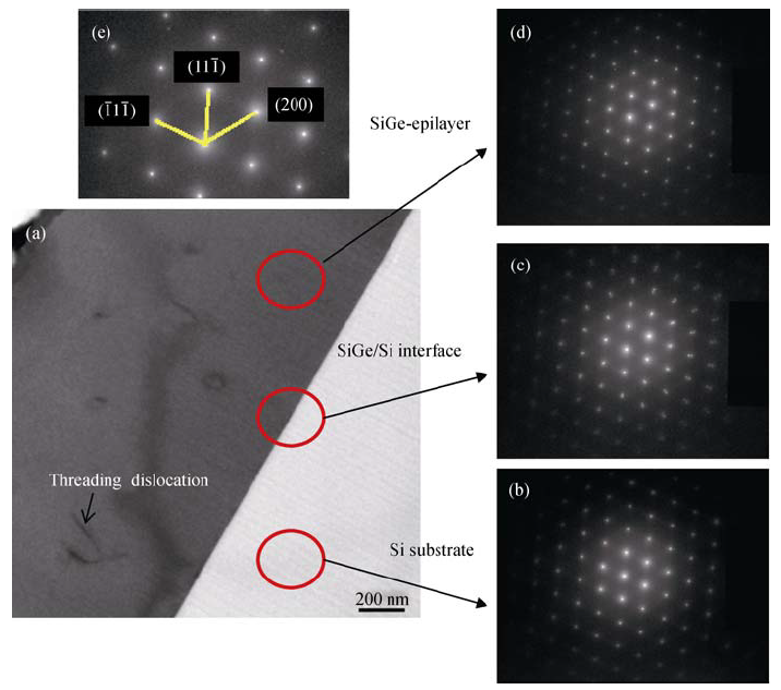
图1 硅锗外延薄膜的断面透射电镜照片(a)及样品不同深度的电子衍射谱(b~d)
Fig. 1 (a) Cross-sectional TEM image of epitaxial SiGe films on silicon substrate, (b)-(d) electron diffraction patterns for Si substrate, SiGe/Si interface and SiGe epilayer (e) which extracted from (d) for calculation The red circles mark the position for measurement of electron diffraction patterns
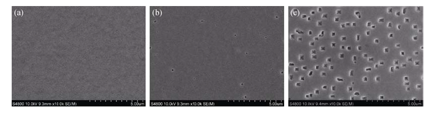
图2 经不同温度退火后硅锗外延薄膜表面的SEM照片
Fig. 2 SEM images of SiGe epilayers annealed at different temperatures(a) 650℃; (b) 700℃; (c) 750℃
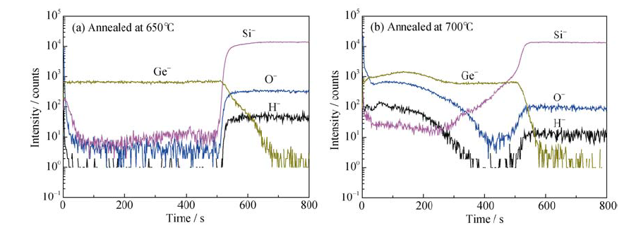
图3 经不同温度退火处理后硅锗外延薄膜由TOF-SIMS测得的离子组分深度分布
Fig. 3 Composition depth profile of ions detected by TOF-SIMS measurement from epitaxial SiGe films annealed at different temperatures
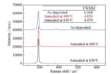
图4 未经退火处理和经退火处理的硅锗外延薄膜的Raman谱图
Fig. 4 Raman spectra of epitaxial SiGe films with or without postannealing
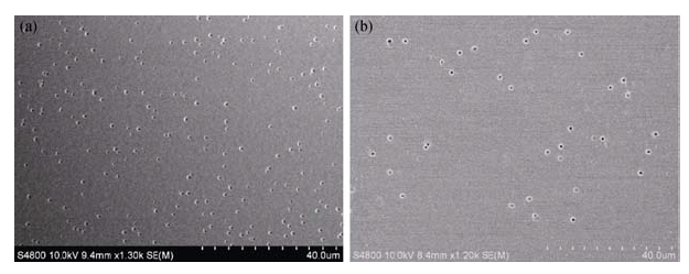
图5 硅锗外延薄膜经选择性湿法腐蚀后的表面扫描电镜照片
Fig. 5 SEM images of SiGe films after a selective wet etch, and pits with reversed pyramidal structure exhibited on the surface(a) As-deposited sample; (b) 650℃-annealed sample
| SixGe1-x | Resistance /(Ω·cm) | Carrier concentration/cm-3 | Mobility/ (cm2·V-1·s-1) |
|---|---|---|---|
| As-grown | 0.402 | 6.35×10¹⁶ | 244 |
| Annealed | 1.470 | 1.07×10¹⁶ | 409 |
表1 由霍尔仪测得的硅锗外延薄膜的电学性能(膜厚900 nm)
Table 1 Electrical properties of SiGe thin films by Hall-effect measurement
| SixGe1-x | Resistance /(Ω·cm) | Carrier concentration/cm-3 | Mobility/ (cm2·V-1·s-1) |
|---|---|---|---|
| As-grown | 0.402 | 6.35×10¹⁶ | 244 |
| Annealed | 1.470 | 1.07×10¹⁶ | 409 |
| Ref. | Temp./℃ | Thickness /nm | RMS roughness/nm | TDD/cm-2 | Mobility/(cm2·V-1·s-1) | |||
|---|---|---|---|---|---|---|---|---|
| As-grown | Annealed | As-grown | Annealed | Annealed | ||||
| [21] | LT | 400 | 1224 | 0.40 | 0.7 | 1.70×10⁸ | 1.00×10⁷ | NA |
| HT | 670 | |||||||
| [22] | LT | 350 | 50 | 0.70 | NA | 5.00×10⁵ | NA | 550 |
| HT | 600 | 300 | ||||||
| [23] | LT | 335 | 2000 | 0.60 | 1.6 | NA | 2.00×10⁷ | NA |
| HT | 670 | |||||||
| [24] | LT | 400 | 2500 | 1.20 | 1.0 | NA | 6.00×10⁶ | NA |
| HT | 750 | |||||||
| [25] | LT | 400 | 980 | 3.19 | 0.9 | NA | 6.00×10⁶ | NA |
| HT | 670 | |||||||
表2 文献中报道的采用低温/高温法制备的锗外延薄膜的性能参数
Table 2 Summary of the process parameters and film quality from literatures which reported the epitaxial growth of Ge by using low temperature/high temperature method
| Ref. | Temp./℃ | Thickness /nm | RMS roughness/nm | TDD/cm-2 | Mobility/(cm2·V-1·s-1) | |||
|---|---|---|---|---|---|---|---|---|
| As-grown | Annealed | As-grown | Annealed | Annealed | ||||
| [21] | LT | 400 | 1224 | 0.40 | 0.7 | 1.70×10⁸ | 1.00×10⁷ | NA |
| HT | 670 | |||||||
| [22] | LT | 350 | 50 | 0.70 | NA | 5.00×10⁵ | NA | 550 |
| HT | 600 | 300 | ||||||
| [23] | LT | 335 | 2000 | 0.60 | 1.6 | NA | 2.00×10⁷ | NA |
| HT | 670 | |||||||
| [24] | LT | 400 | 2500 | 1.20 | 1.0 | NA | 6.00×10⁶ | NA |
| HT | 750 | |||||||
| [25] | LT | 400 | 980 | 3.19 | 0.9 | NA | 6.00×10⁶ | NA |
| HT | 670 | |||||||
| [1] | PAUL D J.Silicon-germanium strained layer materials in microelectronics.Advanced Materials, 1999, 11(17): 191-204. |
| [2] | CHANG S T, LIAO M H, LIN W K.Si/SiGe hetero-junction solar cell with optimization design and theoretical analysis.Thin Solid Films, 2011, 519(15): 5022-5025. |
| [3] | HADI S A,HASHEMI P, NAYFEH A,et al. Thin film a-Si/c- Si1-xGex/c-Si heterojunction solar cells: design and material quality requirements, thin-film si cells.ECS Transactions, 2011, 41(4): 3-14. |
| [4] | CANNON D D, LIU J, DANIELSON D T,et al. Germanium-rich silicon-germanium films epitaxially grown by ultrahigh vacuum chemical-vapor deposition directly on silicon substrates.Applied Physics Letters, 2007, 91(25): 252111. |
| [5] | CHEN J X, ERNST F, HANSSON P O,et al. Liquid phase epitaxy of GeSi on {111} Si substrates: lattice defect structure and electronic properties.Journal of Crystal Growth, 1992, 118(s 3-4): 452-460. |
| [6] | CURRIEM T, SAMAVEDAM S B, LANGDO T A,et al. Controlling threading dislocation densities in Ge on Si using graded SiGe layers and chemical-mechanical polishing.Applied Physics Letters, 1998, 72(14): 1718-1720. |
| [7] | LOH T H, NGUYEN H S, TUNG C H, et al.Ultrathin low temperature SiGe buffer for the growth of high quality Ge epilayer on Si(100) by ultrahigh vacuum chemical vapor deposition.Applied Physics Letters.2007, 90(90): 092108-1-3. |
| [8] | GUO L, ZHAO S, WANG J,et al. Fabrication of strained Ge film using a thin SiGe virtual substrate.Journal of Semiconductors, 2009, 30(9): 16-20. |
| [9] | LOO R, SOURIAU L, ONG P,et al. Smooth and high quality epitaxial strained Ge grown on SiGe strain relaxed buffers with 70-85% Ge.Journal of Crystal Growth, 2011, 324(1): 15-21. |
| [10] | CHOI D, GE Y, HARRIS J S,et al. Low surface roughness and threading dislocation density Ge growth on Si (001) .Journal of Crystal Growth, 2008, 310(18): 4273-4279. |
| [11] | KIM H-W, SHIN K W, LEE G D,et al. High quality Ge epitaxial layers on Si by ultrahigh vacuum chemical vapor deposition.Thin Solid Films, 2009, 517(14): 3990-3994. |
| [12] | YAMAMOTO M, HANNA J, MIYAUCHI M.New low pressure chemical vapor deposition technique for Ge crystalline thin films.Applied Physics Letter, 1993, 63(18): 2508-2510. |
| [13] | YAMAMOTO M, TAKADA Y, HANNA J.Selective growth of Ge in GeF4-Si2H6 system.Applied Physics Letter, 1994, 64(25): 3467-3469. |
| [14] | HANNA J, SHIMIZU K.Low-temperature growth of polycrystalline Si and Ge films by redox reactions of Si2H6 and GeF4.Journal of Organometallic Chemistry, 2000, 611(1): 531-536. |
| [15] | TAO K, KUROSAWA Y, HANNA J.Low-temperature epitaxial growth of high quality Si1-xGex (x≥0.99) films on Si(001) wafer by reactive thermal chemical vapor deposition.Applied Physics Letters, 2013, 102: 182109-1-5. |
| [16] | NAYFEH A, CHUI C O, SARASWATK C,et al. Effects of hydrogen annealing on heteroepitaxial-Ge layers on Si: surface roughness and electrical quality.Applied Physics Letters, 2004, 85(14): 2815-2817. |
| [17] | HARTMANN J M, ABBADIEA,BARNES J P,et al.Impact of the H2 anneal on the structural and optical properties of thin and thick Ge layers on Si; low temperature surface passivation of Ge by Si.Journal of Crystal Growth, 2010, 312(4): 532-541. |
| [18] | KOBAYASHI S, NISHI Y, SARASWAT K C.Effect of isochronal hydrogen annealing on surface roughness and threading dislocation density of epitaxial Ge films grown on Si.Thin Solid Films, 2010, 518(6): S136-S139. |
| [19] | LUAN H C, LIM D R, LEE K K,et al. High-quality Ge epilayers on Si with low threading-dislocation densities.Applied Physics Letters, 1999, 75(19): 2909-2911. |
| [20] | PEZZOLI F, BONERA E, GRILLI E,et al. Raman spectroscopy determination of composition and strain in image heterostructures.Materials Science in Semiconductor Processing, 2008, 11(s 5-6): 279-284. |
| [21] | SHAH V A, DOBBIE A, MYRONOV M,et al. High quality relaxed Ge layers grown directly on a Si(001) substrate.Solid-State Electronics, 2011, 62(1): 189-194. |
| [22] | ZHOU Z, LI C, LAI H,et al. The influence of low-temperature Ge seed layer on growth of high-quality Ge epilayer on Si(100) by ultrahigh vacuum chemical vapor deposition.Journal of Crystal Growth, 2008, 310(10): 2508-2513. |
| [23] | OLUBUYIDE O O, DANIELSON D T,KIMERLING L C,et al. Impact of seed layer on material quality of epitaxial germanium on silicon deposited by low pressure chemical vapor deposition.Thin Solid Films, 2006, 508(1): 14-19. |
| [24] | HARTMANN J M, DAMLENCOURT J F, BOGUMILOWICZ Y,et al. Reduced pressure-chemical vapor deposition of intrinsic and doped ge layers on Si(001) for microelectronics and optoelectronics purposes.Journal of Crystal Growth, 2005, 274(1/2): 90-99. |
| [25] | TAN Y H, TAN C S.Growth and characterization of germanium epitaxial film on silicon (001) using reduced pressure chemical vapor deposition. Thin Solid Films, 2012, 520(7): 2711-2716. |
| [1] | 王萌萌, 田力, 张俊敏, 李庆刚, 杨金山, 董绍明. 3D打印制备CNT/SiC-SiO2及其电磁屏蔽性能[J]. 无机材料学报, 2026, 41(6): 831-838. |
| [2] | 洪恩柳, 涂欣晨, 李自清, 方晓生. 二维钙钛矿单晶纳米片的漂浮法制备及其光电探测性能[J]. 无机材料学报, 2026, 41(6): 787-794. |
| [3] | 李涵涛, 沈强, 罗国强, 王雪飞, 高明, 陈晨. 机械球磨法调控硅基负极材料结构与性能的研究进展[J]. 无机材料学报, 2026, 41(5): 561-572. |
| [4] | 钱新宇, 王无敌, 郭俊尧, 任永春, 董建树, 王庆国, 唐慧丽, 张晨波, 徐晓东, 董永军, 华伟, 徐军. Ho:BaF2晶体在近红外-中红外波段光谱性能分析[J]. 无机材料学报, 2026, 41(5): 595-603. |
| [5] | 朱开煌, 杨世杰, 李欣格, 宋贯卿, 史淦升, 王焱, 任小孟, 陆遥, 徐新宏, 孙静. 基于UiO-66骨架的氧化石墨烯改性金属有机框架凝胶的制备及其对甲苯的高效吸附性能[J]. 无机材料学报, 2026, 41(4): 519-526. |
| [6] | 蒋圣楠, 郑重, 何唯一, 刘涛, 潘秀红, 陈锟, 郭辉, 高攀, 刘春俊, 刘学超. 硼镓共掺氧化锌透明电极的制备及性能优化[J]. 无机材料学报, 2026, 41(4): 479-485. |
| [7] | 徐浩, 顾海涛, 吴鸿辉, 岳晓飞, 林思琪, 金敏. Bi掺杂InSe晶体生长及性能研究[J]. 无机材料学报, 2026, 41(4): 493-499. |
| [8] | 张梦婕, 李智博, 黄瑞楠, 吕向菲, 王伟. 堇青石/硼酸铝晶须/Co0.8FexCe0.2-xCr2O4催化剂的制备及其碳烟过滤-催化燃烧性能[J]. 无机材料学报, 2026, 41(4): 509-518. |
| [9] | 隋金洋, 周大雨, 赵文瑾, 童祎, 王新朋. 工作气压对AlScN薄膜结构和电学性能的影响[J]. 无机材料学报, 2026, 41(4): 486-492. |
| [10] | 程澳芃, 王跃文, 许文涛, 刘全伟, 张海涛, 周有福. 吸附-沉淀自组装结合放电等离子烧结法制备石墨烯增强氧化铝复合陶瓷[J]. 无机材料学报, 2026, 41(4): 536-544. |
| [11] | 李璇, 叶奎材, 冯佳音, 邱家军, 钱文昊, 邢敏. 钛基牙种植体表面改性促进软组织封闭的研究进展[J]. 无机材料学报, 2026, 41(4): 432-444. |
| [12] | 王禹贺, 罗颐秀, 郭会明, 张广珩, 张思岩, 孙鲁超, 王杰民, 王京阳. 高熵稀土氧化物热障涂层材料弹性及热物性的第一性原理研究[J]. 无机材料学报, 2026, 41(4): 445-454. |
| [13] | 李泽熙, 卢文杰, 王朝, 张璐, 李述体, 高芳亮. 基于液态金属镓制备二维氮化镓及其光电性能研究[J]. 无机材料学报, 2026, 41(3): 377-384. |
| [14] | 田洪旺, 罗龙飞, 胡成龙, 闫猛, 庞生洋, 李建, 汤素芳. C/CA表面陶瓷-树脂涂层的简易制备与中温抗氧化性能[J]. 无机材料学报, 2026, 41(3): 401-408. |
| [15] | 邓恒杨, 秦翠洁, 郝胜兰, 冯光迪, 朱秋香, 田博博, 褚君浩, 段纯刚. 基于金属-半导体-金属鳍式隧穿二极管的高频整流桥电路[J]. 无机材料学报, 2026, 41(2): 253-261. |
| 阅读次数 | ||||||
|
全文 |
|
|||||
|
摘要 |
|
|||||