无机材料学报 ›› 2012, Vol. 27 ›› Issue (5): 449-457.DOI: 10.3724/SP.J.1077.2012.00449 CSTR: 32189.14.SP.J.1077.2012.00449
• • 下一篇
陈长鑫, 金铁凝, 张亚非
收稿日期:2011-09-12
修回日期:2011-11-29
出版日期:2012-05-10
网络出版日期:2012-03-31
基金资助:CHEN Chang-Xin, JIN Tie-Ning, ZHANG Ya-Fei
Received:2011-09-12
Revised:2011-11-29
Published:2012-05-10
Online:2012-03-31
Supported by:摘要:
碳纳米管(CNT)由于其独特结构和优异特性已被广泛用来构筑各种纳米器件. 而CNT与电极间的接触在CNT器件中扮演着重要的作用, 是器件性能的关键影响因素. 采用何种有效的方法来改善CNT与金属电极间的接触一直是CNT器件研究中的一个重要方面. 本文综述了近年来CNT/金属接触改善方法的研究进展, 结合本课题组的研究对目前有代表性的接触改善方法进行介绍. 阐述了各种改善方法的原理和加工工艺, 讨论了采用这些方法获得的接触特性和器件性能, 并对各方法的特点进行了比较.
中图分类号:
陈长鑫, 金铁凝, 张亚非. 碳纳米管/金属接触改善方法的研究进展[J]. 无机材料学报, 2012, 27(5): 449-457.
CHEN Chang-Xin, JIN Tie-Ning, ZHANG Ya-Fei. Progress in Improvement Methods of Carbon Nanotube/Metal Contact[J]. Journal of Inorganic Materials, 2012, 27(5): 449-457.

图1 (a) 退火后TiC与SWCNT束接触处的HRTEM照片[2]; (b)退火前后SWCNT束的I-V特性曲线[2]
Fig. 1 (a) HRTEM image of the contact interface of TiC and SWCNT bundle after annealing[2]; (b) I-V curves of a SWCNT bridging two Ti pads (as illustrated in the inset) before and after annealing[2]

图2 覆盖于SWCNT上的Ti膜的XRD峰随退火温度的变化[4]
Fig. 2 Evolution of the XRD of a titanium film covering SWCNTs dispersed on a SiO2/Si substrate as a function of temperature[4]
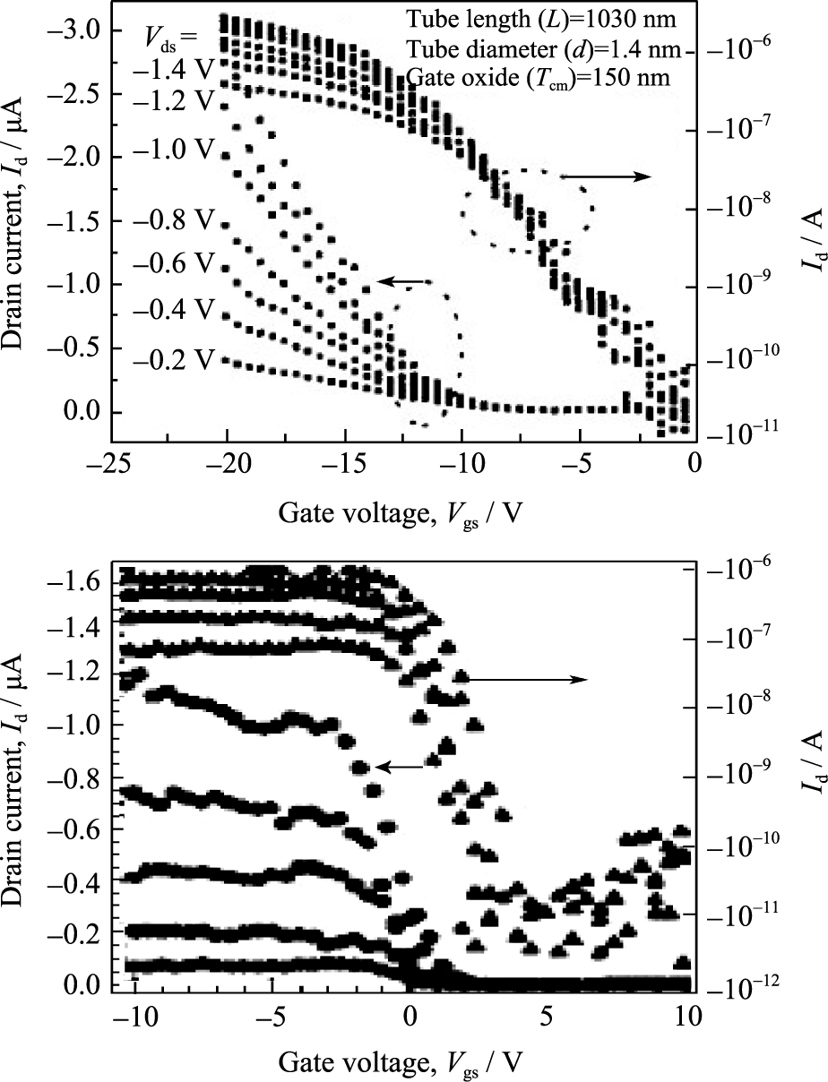
图3 (a)Co电极CNTFET的Id-Vgs曲线(图中右侧曲线为Id-Vgs的对数关系曲线); (b)Ti电极CNTFET的Id-Vgs曲线(图中右侧为lgId-Vgs关系曲线)[3]
Fig. 3 Id-Vgs curves of the Co contacted CNTFET (a) and the Ti contacted CNTFET (b); The right curves in the figures are the logarithmic plot of Id-Vgs characteristics[3]
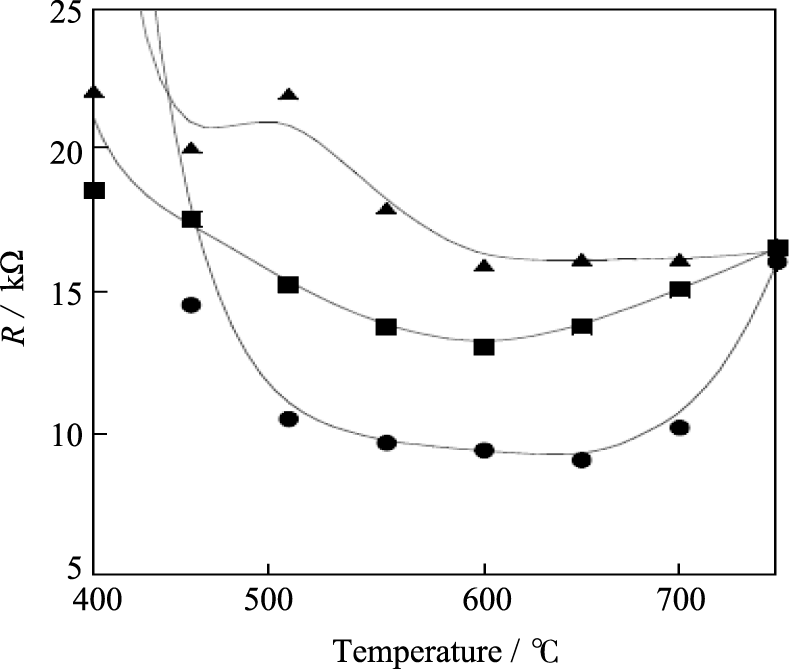
图4 三个样品CNT二端电阻随热处理温度的关系图[7]
Fig. 4 Contact resistance as a function of the rapid thermal annealing (RTA) tem-perature for three different nanotube–Ti–Au electrodes[7]

图5 电脉冲处理过程示意图[15]
Fig. 5 A schematic diagram of the apparatus for the local CNT/electrode contact treatment using an electrical pulse shot[15]
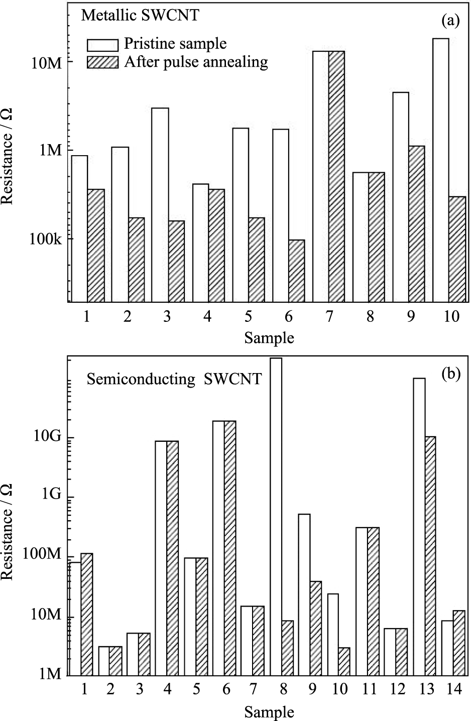
图6 金属性(a)和半导体性(b)SWCNT退火前(空白区)与退火后(阴影区)的二端电阻[15]
Fig. 6 Statistics of the changes in the 2-terminal resistance before (blank) and after (shadow) pulse annealing for the cases of an individual (a) metallic SWCNT and (b) semiconducting SWCNT[15]
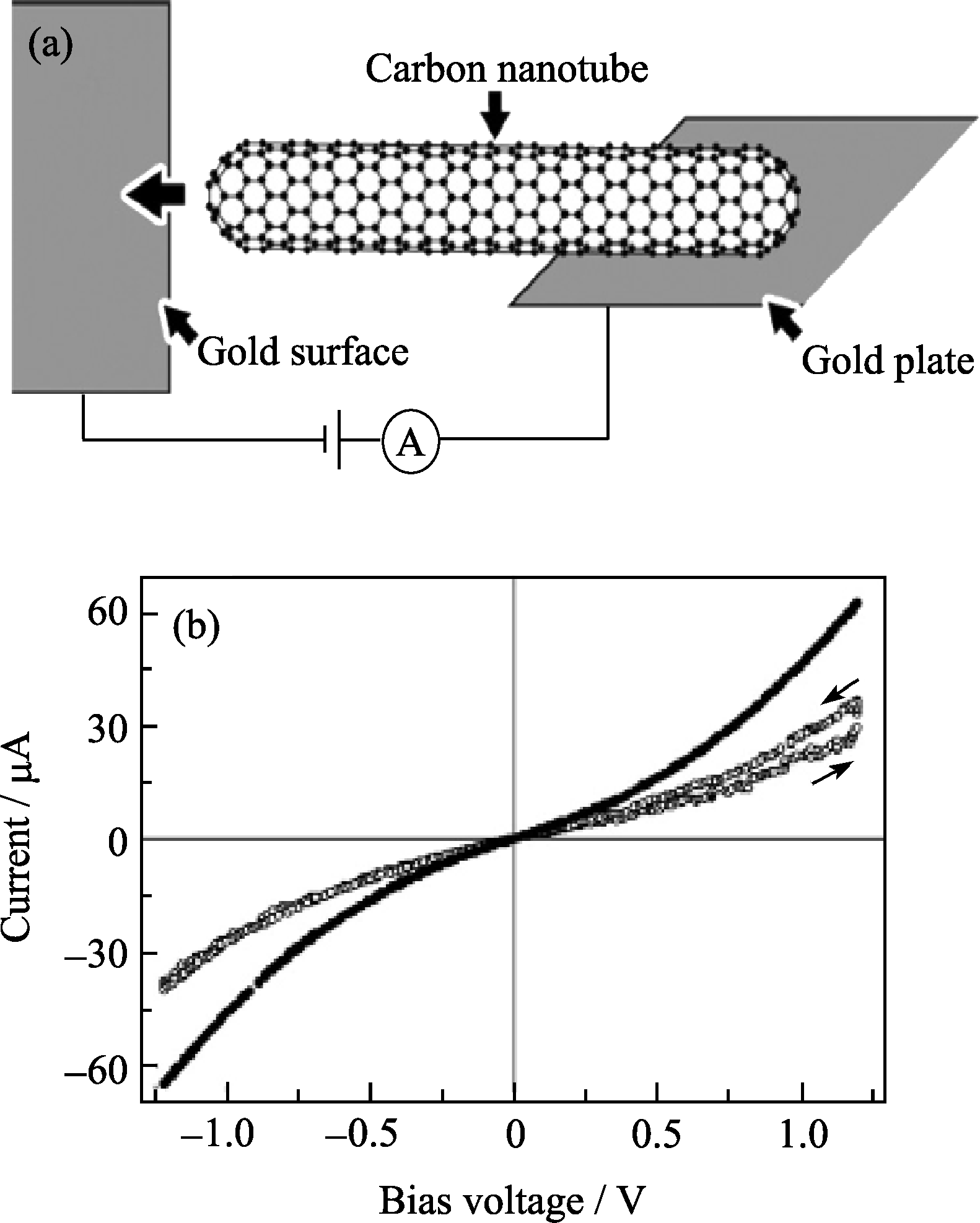
图7 (a) CNT末端移向金电极表面过程示意图[16]; (b) 空心和实心点线分别为MWCNT与金电极刚接触上和加电压一段时间嵌入金电极表面后的I-V曲线[16]
Fig. 7 (a) Illustration of the procedure for connecting a carbon nanotube to a gold surface[16]; (b) Current-voltage curves for two different contact states: open circles are data obtained when the MWCNT tip is just in contact with the gold surface and filled circles are for when the tip is embedded in the gold surface[16]

图8 (a)电子束沉积处理过程示意图; (b)流经CNT的电流随电子束沉积时间变化的曲线图[26]
Fig. 8 (a) Schematic diagram of the process of electron beam deposition; (b) Current vs deposition time during soldering of the MWCNT using the electron beam[26]
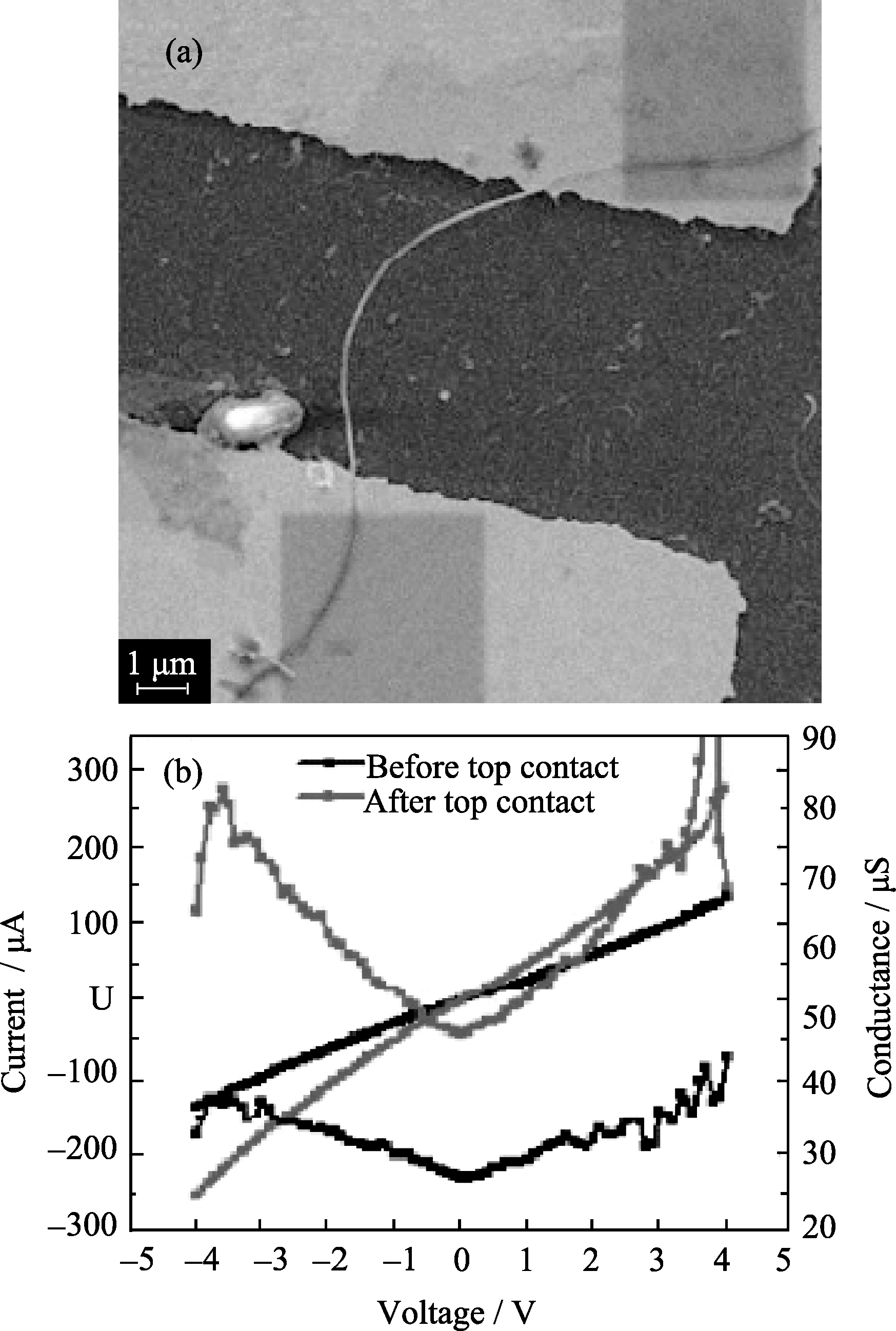
图9 (a) 电子束沉积法处理后CNT与金电极接触处的SEM照片; (b) 电子束沉积法处理前(黑)和处理后(灰)CNT的I-V与G-V特性[27]
Fig. 9 (a) The SEM image of the contacts of CNT and gold pads after top metal deposition; (b) The I-V and G-V curves before (black) and after (gray) the electron beam deposition[27]
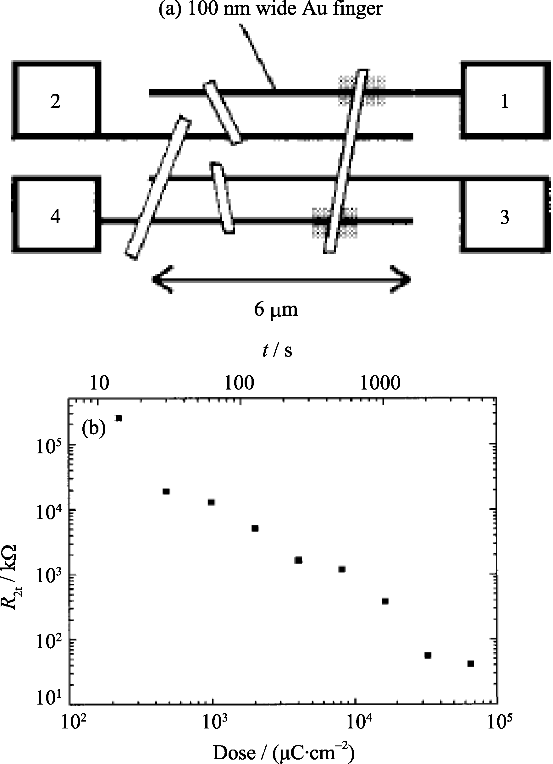
图10 (a)电子束辐照CNT与金电极接触处的示意图, 阴影区为电子束辐射区域[29]; (b) CNT二端电阻与电子束辐照剂量的关系图[29]
Fig. 10 (a) Schematic of exposing the CNT/Au contacts under electron beam. The shadows show the areas of electron beam irritation[29]; (b) Two-terminal resistance R2t as a function of electron exposure dose in SEM[29]
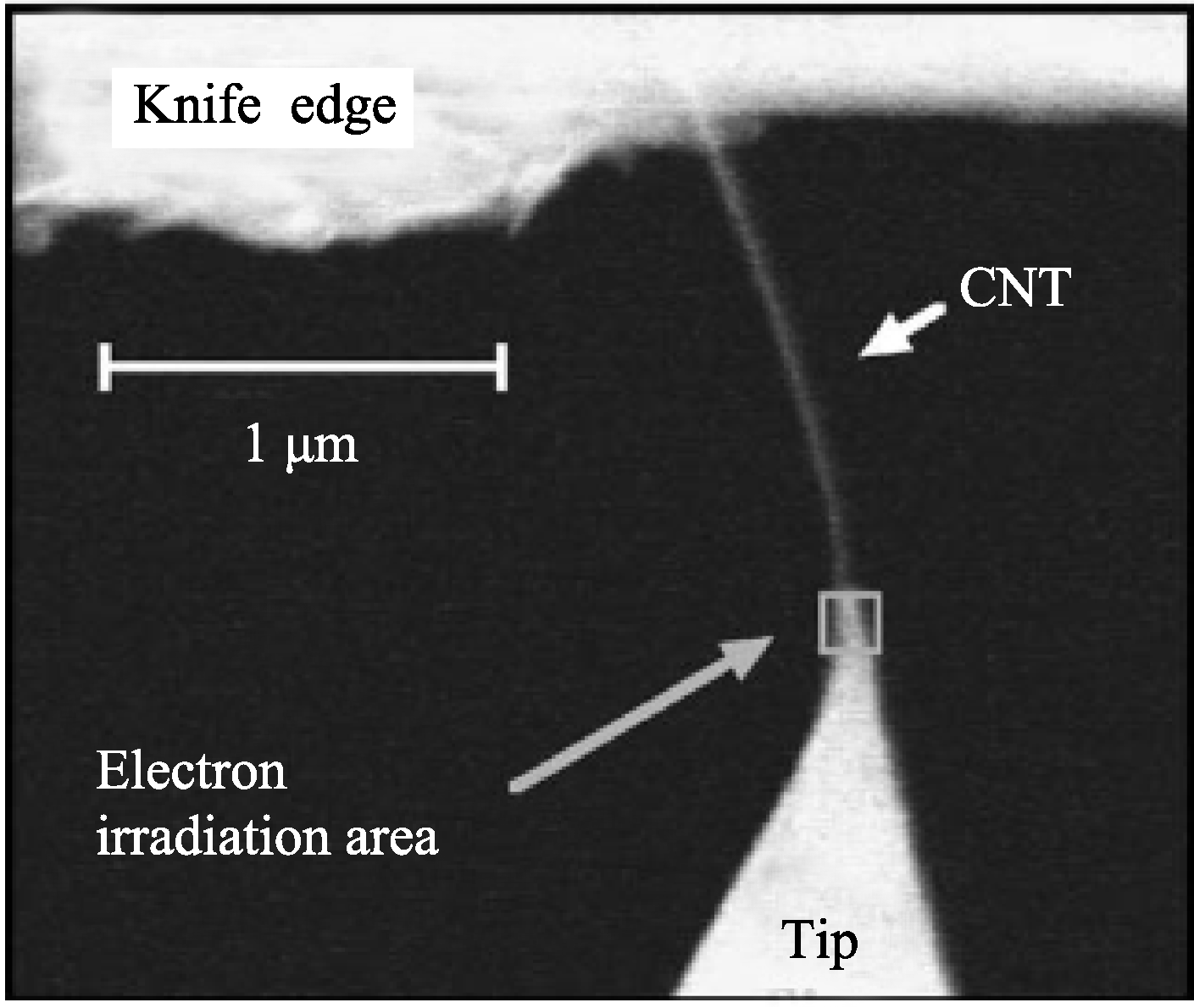
图11 CNT与硅悬臂梁表面的Pt金属在电子束辐照改善接触后的SEM照片[30]
Fig. 11 SEM image of the contact between CNT and metal Pt on Si cantilever surface after electron beam irradiation[30]
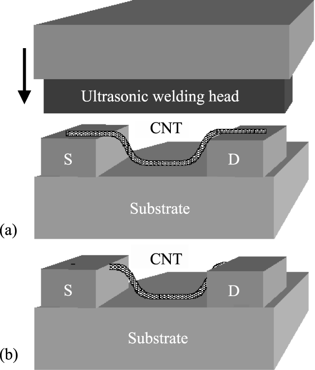
图12 超声纳米焊接工艺示意图[32]
Fig. 12 Schematic diagrams of the ultrasonic nanowelding process[32] (a) Before welding; (b) After welding
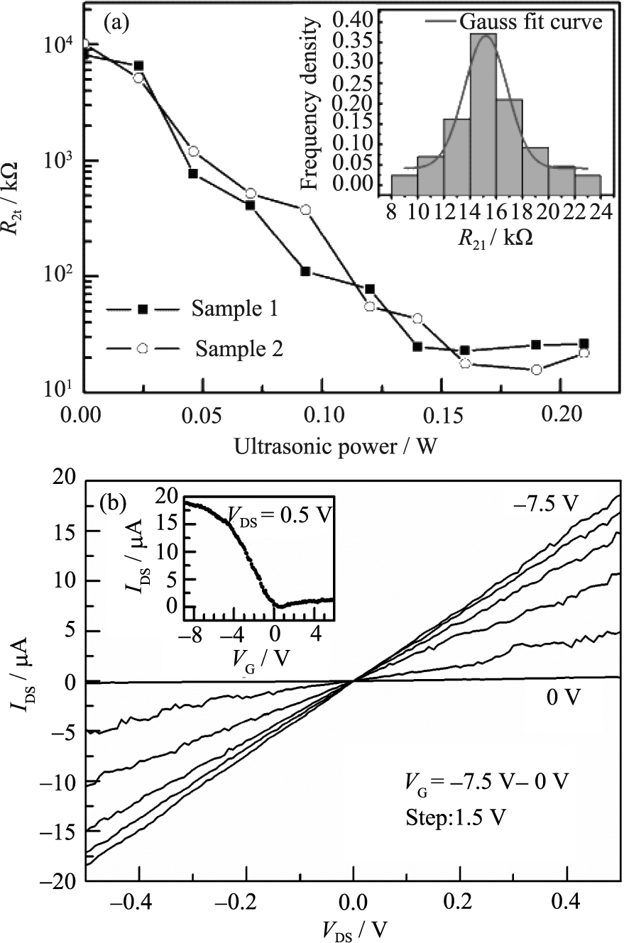
图13 (a) 金属性SWCNT的二端电阻值随超声焊接功率的变化关系; 插图为对43个样品焊接后得到的最低二端电阻值进行统计分析和分布拟合, 得出焊接后最低电阻主要集中在15 kΩ左右[32]; (b) 制作的CNTFET的输出特性曲线; 插图为其转移特性曲线[32]
Fig. 13 (a) Two-terminal (2t-) resistance as a function of the ultrasonic power for two metallic nanotube; Inset: the statistical analysis and distribution fit of the obtained lowest 2t-resistances for 43 samples after nanowelding, which indicates that the lowest resistance is about 15 kΩ[32]; (b) Output characteristic of the fabricated CNTFET. Inset: transfer characteristic curve[32]
| [1] | Avouris P, Hertel T, Martel R, et al. Carbon nanotubes nanomechanics, manipulation, and electronic devices. Applied Surface Science, 1999, 141(3/4): 201-209. |
| [2] | Zhang Y, Ichihashi T, Landree E, et al. Heterostructrues of single-walled carbon nanotubes and carbide nanorods. Science, 1999, 285(5434): 1719-1720. |
| [3] | Martel R, Wong H S P, Chan K, et al. Carbon Nanotube Field Effect Transistors for Logic Application. IEDM Technical Digest, 2001: 159-162. |
| [4] | Martel R, Derycke V, Lavoie C, et al. Ambipolar electrical transport in semiconducting single-wall carbon nanotubes. Physical Review Letters, 2001, 87(25): 256805-1-4. |
| [5] | Avouris P, Appenzeller J, Martel R, et al. Carbon nanotube electronics. Proceedings of IEEE, 2003, 91(11): 1772-1784. |
| [6] | Avouris P, Martel R, Derycke V, et al. Carbon nanotube transistors and logic circuits. Physica B, 2003, 323(1-4): 6-14. |
| [7] | Lee J O, Park C, Kim J J, et al. Formation of low-resistance ohmic contacts between carbon nanotube and metal electrodes by a rapid thermal annealing method. Journal of Physics D:Applied Physics, 2000, 33(16):1953-1956. |
| [8] | Kane A, Sheps T, Branigan E, et al. Contacts to metallic single-walled carbon nanotubes using Pt electrodes. Nano Letters, 2009, 9(10): 3586-3591. |
| [9] | Bhuvana T, Smith K, Fisher T, et al. Self-assembled CNT circuits with ohmic contacts using Pd hexadecanethiolate as in situ solder. Nanoscale, 2009, 1(2): 271-275. |
| [10] | Roschier L, Tarkiainen R, Ahlskog M. Manufacture of single electron transistors using AFM manipulation on multiwalled carbon nanotubes. Microelectronic Engineering, 2002, 61-62: 687-691. |
| [11] | Huang L, Chor E F, Wu Y, et al. Investigations of niobium carbide contact for carbon-nanotube-based devices. Nanotechnology, 2010, 21(9): 095201. |
| [12] | Tan M M, Ye X Y, Wang X H, et al. Improving contact of CNT-metal by annealing. Journal of Functional Materials and Devices, 2008, 14(1): 227-230. |
| [13] | Hobara R, Yoshimoto S, Ikuno T, et al. Electronic transport in mutiwalled carbon nanotubes contacted with patterned electrodes. Japanese Journal of Applied Physics, 2004, 43(8B): 1081-1084. |
| [14] | Hsiou Y, Yang Y J, Stobinski L, et al. On the Ohmic contact between multiwalled carbon nanotubes and nano-electrodes. Chinese Journal of Physics, 2005, 43(1-II): 293-297. |
| [15] | Woo Y S, Duseberg G, Roth S. Reduced contact resistance between an individual single-walled carbon nanotube and a metal electrode by a local point annealing. Nanotechnology, 2007, 18(9): 095203-1-3. |
| [16] | Asaka K, Karita M, Saito Y. Modification of interface structure and contact resistance between a carbon nanotube and a gold electrode by local melting. Applied Surface Science, 2011, 257(7): 2850-2853. |
| [17] | Dong L F, Youkey S, Bush J, et al. Effect of local joule heating on the reduction contact resistance between carbon nanotubes and metal electrodes. Journal of Applied Physics, 2007, 101(2): 024320-1-7. |
| [18] | Tian X J, Wang Y C, Dong Z L. A Study on the assembly and improovement of electrical contact between carbon nanotube and microelectrode. Advanced Materials Research, 2009, 60-61: 399-405. |
| [19] | Maki H, Masaki S, Ishibashi J. Local change of carbon nanotube- metal contacts by current flow through electrodes. Japanese Journal of Applied Physics, 2004, 43(4B) : 2027-2030. |
| [20] | Yamada T, Saito T, Suzuki M, et al. Tunneling between carbon nanofiber and gold electrodes. Journal of Applied Physics, 2010, 107(4) : 044304-1-5. |
| [21] | Dong L F, Chirayos V, Bush J, et al. Floating-potential dielectrophoresis-controlled fabrication of single-carbon-nanotube transistors and their electrical properties. Journal of Physics Chemisty B, 2005, 109(27) : 13148-13153. |
| [22] | Woo Y S, Roth S. Effect of Contact Improvement on the FET Characteristics of an Individual Single Walled Carbon Nanotube. AIP Conference Proceeding, 2005, 786: 566-569. |
| [23] | Tsutsui M, Taninouchi Y, Kurokawa S, et al. Bias-induced local heating effects on multi-walled carbon nanotube-Au contacts. Japanese Journal of Applied Physics, 2006, 45(1A): 341-345. |
| [24] | Wang M S, Golberg D, Bando Y. Superstrong low-resistant carbon nanotube-carbide-metal nanocontacts. Advanced Materials, 2010, 22(47): 5350-5355. |
| [25] | Chen Q, Wang S, Peng L M. Establishing Ohmic contacts for in situ current-voltage characteristic measurements on a carbon nanotube inside the scanning electron microscope. Nanotechnology, 2006, 17(4): 1087-1098. |
| [26] | Madsen D N, Molhave K, Mateiu R, et al. Solding of nanotubes onto microelectrodes. Nano Letters, 2003, 3(1): 47-49. |
| [27] | Neha K, Misra A, Srinivasan S, et al. Effect of top metal contact on electrical transport through individual multiwalled carbon nanotube. Applied Physics Letters, 2010, 97(22): 222102-1-3. |
| [28] | Tersoff J. Contact resistance of carbon nanotubes. Applied Physics Letters, 1999, 74(15): 2122-2124. |
| [29] | Bachtold A, Henny M, Terrier C, et al. Contacting carbon nanotubes selectively with low-ohmic contacts for four-probe electric measurements. Applied Physics Letters, 1998, 73(2): 274-276. |
| [30] | Ando A, Shimizu T, Abe H, et al. Improvement of electrical contact at carbon nanotube/Pt by selective electron irradiation. Physica E, 2004, 24(1/2): 6-9. |
| [31] | Rodriguez-Manzo J, Banhart F, Terrones M, et al. Heterojunctions between metals and carbon nanotubes as ultimate nanocontacts. Applied Physical Science, 2009, 106(12): 4591-4595. |
| [32] | Chen C X, Yan L J, Kong E S, et al. Ultrasonic nanowelding of carbon nanotubes to metal electrodes. Nanotechnology, 2006, 17(9): 2192-2197. |
| [33] | Chen C X, Liu L Y, Lu Y, et al. A method for creating reliable and low-resistance contacts between carbon nanotubes and microelectrodes. Carbon, 2007, 45(2): 436-442. |
| [34] | Chen C X, Xu D, Kong E S, et al. Multichannel carbon-nanotube FETs and complementary logic gates with nanowelded contacts. IEEE Electron Device Letters, 2006, 27(10): 852-855. |
| [35] | Chen C X, Zhang W, Zhang Y F. Multichannel carbon nanotube field-effect transistors with compound channellayer. Applied Physics Letters, 2009, 95(19): 192110-1-3. |
| [36] | Chen C X, Lu Y, Kong E S, et al. Nanowelded carbon-nanotube- based solar microcells. Small, 2008, 4(9): 1313-1318. |
| [37] | Chen C X, Zhang W, Kong E S, et al. Carbon nanotube photovoltaic device with asymmetrical contacts. Appllied Physics Letters, 2009, 94(26): 263501-1-3. |
| [38] | Lim S C, Jang J H, Bae D J, et al. Contact resistance between metal and carbon nanotube interconnects:effect of work function and wettability. Applied Physics Letters, 2009, 95(26): 264103-1-3. |
| [39] | Song Y J, Kang S J. Improvement of contact resistance between carbon nanotubes and metal electrodes for high performance electronics. J. Vac. Sci. Technol. B, 2010, 29(1): 011011-1-3. |
| [40] | Nirmalraj P N, Boland J J. Selective tuning and optimization of the contacts to metallic and semiconducting single-walled carbon nanotubes. ACS Nano, 2010, 4(7): 3801-3806. |
| [41] | Dockendorf C, Steinlin M, Proulikakos D. Individual carbon nanotube soldering with gold nanoink deposition. Applied Physics Letters, 2007, 90(19): 193116-1-3. |
| [42] | Lee S, Park J Y, Cho Y S, et al. Nanosoldering of carbon nanotubes on metal electrodes with an atomic force microscope. Journal of Vacuum Science and Technology B, 2007, 25(3): 916-1-6. |
| [43] | Liebau M, Unger E, Duesberg G, et al. Contact improvement of carbon nanotubes via electroless nickel deposition. Applied Physics A, 2003, 77(6): 731-734. |
| [44] | Seidel R, Liebau M, Duesberg G.et al. In-situ contacted single- walled carbon nanotubes and contact improvement by electroless deposition. Nano Letters, 2003, 3(7): 965-968. |
| [45] | Leon J, Flacker A, Vaz A, et al. Electrical characterization of multi-walled carbon nanotubes. Journal of Nanoscience andNanotechnology, 2010, 10(9): 6234-6239. |
| [46] | Caillier C, Ayan A, Gouttenoire V, et al. Gold contact to individual metallic carbon nanotubes: asensitive nanosensor for high-pressure. Applied Physics Letters, 2010, 97(17): 173111-1-3. |
| [47] | Kasumov A, Deblock R, Kociak M, et al. Supercurrents through single-walled carbon nanotubes. Science, 1999, 284(5419): 1508-1510. |
| [1] | 魏相霞, 张晓飞, 徐凯龙, 陈张伟. 增材制造柔性压电材料的现状与展望[J]. 无机材料学报, 2024, 39(9): 965-978. |
| [2] | 杨鑫, 韩春秋, 曹玥晗, 贺桢, 周莹. 金属氧化物电催化硝酸盐还原合成氨研究进展[J]. 无机材料学报, 2024, 39(9): 979-991. |
| [3] | 刘鹏东, 王桢, 刘永锋, 温广武. 硅泥在锂离子电池中的应用研究进展[J]. 无机材料学报, 2024, 39(9): 992-1004. |
| [4] | 黄洁, 汪刘应, 王滨, 刘顾, 王伟超, 葛超群. 基于微纳结构设计的电磁性能调控研究进展[J]. 无机材料学报, 2024, 39(8): 853-870. |
| [5] | 陈乾, 苏海军, 姜浩, 申仲琳, 余明辉, 张卓. 超高温氧化物陶瓷激光增材制造及组织性能调控研究进展[J]. 无机材料学报, 2024, 39(7): 741-753. |
| [6] | 王伟明, 王为得, 粟毅, 马青松, 姚冬旭, 曾宇平. 以非氧化物为烧结助剂制备高导热氮化硅陶瓷的研究进展[J]. 无机材料学报, 2024, 39(6): 634-646. |
| [7] | 蔡飞燕, 倪德伟, 董绍明. 高熵碳化物超高温陶瓷的研究进展[J]. 无机材料学报, 2024, 39(6): 591-608. |
| [8] | 吴晓晨, 郑瑞晓, 李露, 马浩林, 赵培航, 马朝利. SiCf/SiC陶瓷基复合材料高温环境损伤原位监测研究进展[J]. 无机材料学报, 2024, 39(6): 609-622. |
| [9] | 赵日达, 汤素芳. 多孔碳陶瓷化改进反应熔渗法制备陶瓷基复合材料研究进展[J]. 无机材料学报, 2024, 39(6): 623-633. |
| [10] | 方光武, 谢浩元, 张华军, 高希光, 宋迎东. CMC-EBC损伤耦合机理及一体化设计研究进展[J]. 无机材料学报, 2024, 39(6): 647-661. |
| [11] | 张幸红, 王义铭, 程源, 董顺, 胡平. 超高温陶瓷复合材料研究进展[J]. 无机材料学报, 2024, 39(6): 571-590. |
| [12] | 张慧, 许志鹏, 朱从潭, 郭学益, 杨英. 大面积有机-无机杂化钙钛矿薄膜及其光伏应用研究进展[J]. 无机材料学报, 2024, 39(5): 457-466. |
| [13] | 李宗晓, 胡令祥, 王敬蕊, 诸葛飞. 氧化物神经元器件及其神经网络应用[J]. 无机材料学报, 2024, 39(4): 345-358. |
| [14] | 鲍可, 李西军. 化学气相沉积法制备智能窗用热致变色VO2薄膜的研究进展[J]. 无机材料学报, 2024, 39(3): 233-258. |
| [15] | 胡梦菲, 黄丽萍, 李贺, 张国军, 吴厚政. 锂/钠离子电池硬碳负极材料的研究进展[J]. 无机材料学报, 2024, 39(1): 32-44. |
| 阅读次数 | ||||||
|
全文 |
|
|||||
|
摘要 |
|
|||||