无机材料学报 ›› 2024, Vol. 39 ›› Issue (3): 233-258.DOI: 10.15541/jim20230386 CSTR: 32189.14.10.15541/jim20230386
• 综述 • 下一篇
鲍可1,2( ), 李西军1,2,3()
收稿日期:2023-08-28
修回日期:2023-09-29
出版日期:2024-03-20
网络出版日期:2023-11-28
通讯作者:
李西军, 研究员. E-mail: lixijun@westlake.edu.cn作者简介:鲍可(1984-), 女, 博士. E-mail: baoke@westlake.edu.cn
基金资助:
BAO Ke1,2(), LI Xijun1,2,3()
Received:2023-08-28
Revised:2023-09-29
Published:2024-03-20
Online:2023-11-28
Contact:
LI Xijun, professor. E-mail: lixijun@westlake.edu.cnAbout author:BAO Ke (1984-), female, PhD. E-mail: baoke@westlake.edu.cn
Supported by:摘要:
热致变色智能窗是通过在玻璃上沉积温度刺激响应型材料, 实现根据环境温度调控窗户玻璃的太阳光透过率, 减少建筑物能耗的节能窗户。二氧化钒(VO2)是一种典型的热致相变材料, 在~68 ℃发生金属-绝缘体相变, 相变前后伴随光学性能的显著变化, 在智能窗等多个领域有潜在的技术应用。然而, 当前VO2基热致变色智能窗的应用仍存在着相变温度(τc)偏高、可见光透过率(Tlum)低和太阳能调节效率(ΔTsol)不足等问题, 无法满足实际建筑节能的需求。为了解决这些问题, 研究人员开展了广泛而深入的工作。化学气相沉积法(Chemical vapor deposition, CVD)能够以合理的成本生产高质量、大面积的VO2薄膜, 受到研究者青睐。本文总结了近年来利用CVD技术制备VO2薄膜的研究进展, 系统介绍常压化学气相沉积、气溶胶辅助化学气相沉积、低压化学气相沉积、金属有机物化学气相沉积、原子层沉积和等离子体增强化学气相沉积等CVD工艺, 分析了反应物种类及比例、反应温度、压力、载体流量等因素对VO2薄膜质量的影响, 并结合元素掺杂、纳米复合薄膜、多层膜结构等对VO2薄膜的性能调控与优化进行总结, 最后对未来等离子体增强化学气相沉积制备VO2薄膜的研究前景做出展望。
中图分类号:
鲍可, 李西军. 化学气相沉积法制备智能窗用热致变色VO2薄膜的研究进展[J]. 无机材料学报, 2024, 39(3): 233-258.
BAO Ke, LI Xijun. Chemical Vapor Deposition of Vanadium Dioxide for Thermochromic Smart Window Applications[J]. Journal of Inorganic Materials, 2024, 39(3): 233-258.

图1 热致变色智能窗[7]
Fig. 1 Schematic of thermochromic smart window[7]

图2 VO2的晶体结构和能带结构
Fig. 2 Schematics of the crystal structures and band structures of VO2 (a, b) Schematic depictions of the crystal structures of the high- temperature tetragonal rutile R phase (a) and low-temperature monoclinic M phase (b)[13]; (c, d) Schematic of the VO2 band structure in the metallic (c) and insulating (d) states[14]

图3 辐射冷却调节智能窗的结构与工作原理[27]
Fig. 3 Structure and concept of an RCRT window[27] (a) Schematic structure of the RCRT window; (b, c) Working principle of RCRT window in summer (b) and winter (c)
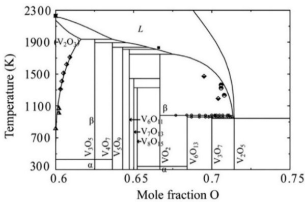
图4 1 atm下V-O系统相图[38]
Fig. 4 Phase diagram of the V-O system at 1 atm[38]

图5 CVD反应过程示意图[72]
Fig. 5 Schematic of general elementary steps of a typical CVD process[72]
| V valence | Compound/Molecular formula | Vapor pressure | Ref. |
|---|---|---|---|
| +3 | V(acac)3/V(C5H7O2)3 | Not volatile, sublimes@220 ℃ | [ |
| +3 | V(amd)3/C24H51N6V | 6.6 Pa@70 ℃, 2.6 Pa@120 ℃ | [ |
| +4 | TDMAV/C8H24N4V | 133 Pa@64 ℃ | [ |
| +4 | TEMAV/C12H32N4V | 13 Pa@25 ℃, 57 Pa@82 ℃, 133 Pa@107 ℃ | [ |
| +4 | VCl4 | 780 Pa@20 ℃, 13.3 kPa@100 ℃ | [ |
| +4 | VO(acac)2/VO(C5H7O2)2 | 0.21 Pa@96 ℃ | [ |
| +4 | VO(thd)2/VO(C11H19O2)2 | 0.27 Pa@96 ℃ | [ |
| +4 | VO(hfa)2/VO(C5H2F6O2)2 | 0.18 Pa@57 ℃ | [ |
| +5 | VO(OC3H7)3 | 6 Pa@20 ℃, 38.6 Pa@45 ℃, 268 Pa@82 ℃ | [[ |
| +5 | VOCl3 | 1.84 kPa@20 ℃, 9.3 kPa@55 ℃ | [ |
表1 CVD制备VO2薄膜采用的钒前驱体的蒸气压
Table 1 Vapor pressure of the vanadium precursorscompounds used for the CVD of VO2 thin films
| V valence | Compound/Molecular formula | Vapor pressure | Ref. |
|---|---|---|---|
| +3 | V(acac)3/V(C5H7O2)3 | Not volatile, sublimes@220 ℃ | [ |
| +3 | V(amd)3/C24H51N6V | 6.6 Pa@70 ℃, 2.6 Pa@120 ℃ | [ |
| +4 | TDMAV/C8H24N4V | 133 Pa@64 ℃ | [ |
| +4 | TEMAV/C12H32N4V | 13 Pa@25 ℃, 57 Pa@82 ℃, 133 Pa@107 ℃ | [ |
| +4 | VCl4 | 780 Pa@20 ℃, 13.3 kPa@100 ℃ | [ |
| +4 | VO(acac)2/VO(C5H7O2)2 | 0.21 Pa@96 ℃ | [ |
| +4 | VO(thd)2/VO(C11H19O2)2 | 0.27 Pa@96 ℃ | [ |
| +4 | VO(hfa)2/VO(C5H2F6O2)2 | 0.18 Pa@57 ℃ | [ |
| +5 | VO(OC3H7)3 | 6 Pa@20 ℃, 38.6 Pa@45 ℃, 268 Pa@82 ℃ | [[ |
| +5 | VOCl3 | 1.84 kPa@20 ℃, 9.3 kPa@55 ℃ | [ |

图6 APCVD装置示意图[36]
Fig. 6 Schematic diagram for APCVD system[36]

图7 APCVD以不同VCl4和H2O比例在450 ℃制备的氧化钒薄膜[90]
Fig. 7 Vanadium oxide thin films grown by APCVD at 450 ℃ using different gas precursor ratios[90] (a) XRD patterns for the samples grown using VCl4: H2O ratios of 1 : 1, 1 : 2 and 1 : 3; (b-d) SEM images of as-deposited (b) V2O3, (c) VO2 and (d) V2O5 thin films

图8 VO(acac)2和不同氧化剂通过APCVD反应生成的VO2薄膜的SEM照片(沉积温度500 ℃)[96]
Fig. 8 FE-SEM images of VO2 films obtained via APCVD with VO(acac)2 and different oxygen sources at 500 ℃[96] VO2 obtained using (a) ethanol; (b) propanol; (c) O2 gas

图9 外电场辅助APCVD装置示意图[97]
Fig. 9 Schematic of electric field EAAPCVD rig[97]
| Vanadium precursor | Bubbler temperature/℃ | Oxygen source | Precursor ratio | Substrate temperature/℃ | Carrier gas flow (N2)/ (L·min-1) | *τc of VO2/℃ | Ref. |
|---|---|---|---|---|---|---|---|
| VCl4 | 100 | H2O | 1 : 10 | 350-550 | 0.2 | 68 | [ |
| VCl4 | 80 | H2O | (0.43-1.08) : 1 | 350-450 | 12 | - | [ |
| VCl4 | 80 | C4H8O2 | 2 : 1 | 550 | 23.2 | 68 | [ |
| VOCl3 | 90 | H2O | 1.0 : 3.4 | 350-650 | 1.0 | 67 | [ |
| VO(acac)2 | 200 | O2 | - | 500-575 | 0.4 | 51.5 | [ |
| VO(OC3H7)3 | 50 | - | - | 450 | 3-4 | 65.5 | [ |
表2 APCVD制备VO2薄膜的工艺条件
Table 2 Range of conditions for the vanadium oxide thin films prepared by APCVD
| Vanadium precursor | Bubbler temperature/℃ | Oxygen source | Precursor ratio | Substrate temperature/℃ | Carrier gas flow (N2)/ (L·min-1) | *τc of VO2/℃ | Ref. |
|---|---|---|---|---|---|---|---|
| VCl4 | 100 | H2O | 1 : 10 | 350-550 | 0.2 | 68 | [ |
| VCl4 | 80 | H2O | (0.43-1.08) : 1 | 350-450 | 12 | - | [ |
| VCl4 | 80 | C4H8O2 | 2 : 1 | 550 | 23.2 | 68 | [ |
| VOCl3 | 90 | H2O | 1.0 : 3.4 | 350-650 | 1.0 | 67 | [ |
| VO(acac)2 | 200 | O2 | - | 500-575 | 0.4 | 51.5 | [ |
| VO(OC3H7)3 | 50 | - | - | 450 | 3-4 | 65.5 | [ |

图10 AACVD的工作原理和系统构成[36,100]
Fig. 10 Mechanism and system configuration for AACVD[36,100]

图11 通过AACVD在400~750 ℃下以不同VO(acac)2溶液制备的VO2薄膜以及基底[9]
Fig. 11 Substrates and VO2 films deposition via AACVD at 400-750 ℃ using different solutions of VO(acac)2[9] (a, c) Photographs (a) and XRD patterns (c) of VO2 films from methanol solution of VO(acac)2; (b, d) Photographs (b) and XRD patterns (d) of VO2 films from water solution of VO(acac)2

图12 通过AACVD以VO(acac)2水溶液为前驱体在650 ℃制得的VO2薄膜的SEM照片[9]
Fig. 12 SEM images of the VO2 films deposited via AACVD at 650 ℃ using a water solution of VO(acac)2[9] (a) Surface SEM image of the VO2 films at low magnification; (b) Surface SEM image of the VO2 films at high magnification; (c) Cross-sectional SEM image of the VO2 films
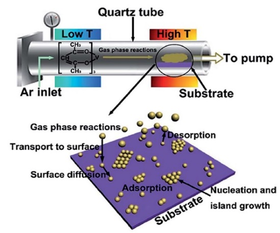
图13 LPCVD装置及沉积过程示意图[103]
Fig. 13 Schematic representation of LPCVD and the CVD reaction process[103]

图14 LPCVD以V(acac)3为前驱体在不同时间下制得的VO2薄膜(350 ℃下沉积30~120 min, 并在350 ℃下退火2 h)[103]
Fig. 14 VO2 films deposited via LPCVD from V(acac)3 at 350 ℃ for 30-120 min and then annealed at 350 ℃ for 2 h[103] (a) Raman spectra of VO2 films; (d) XRD patterns of VO2 films; (b, c, e, f) SEM photographs of VO2 films deposited for (b) 30, (c) 60, (e) 90, and (f) 120 min, respectively
| Vanadium precursor | Evaporator temperature/℃ | Reactor pressure/Pa | Substrate temperature/℃ | O2 flow | Carrier gas flow (Ar) | τc of VO2/℃ | Ref. |
|---|---|---|---|---|---|---|---|
| VO(acac)2 | 150-175 | 2000 | 475-520 | 20-60 sccm | 50-100 sccm | 66-72 | [ |
| VO(acac)2/methanol | 150 | 101325 | 375-450 | 0.02-0.08 L/min | 0.98 L/min | 60 | [ |
| VO(acac)2 | 120-150 | 266.6 | 390-490 | Flow rate of O2 to Ar 0.2 | - | 62±1 | [ |
| VO(acac)2 | 170 | 399.9 | 200-750 | 150 sccm | 150 sccm | - | [ |
| VO(acac)2 | 185 | 2559.36 | 520-550 | 50 sccm | 100 sccm | 61.0-68.5 | [ |
| VO(hfa)2/H2O | 100-120 | 350 | 390-600 | - | 3.6-5.0 L/h | 60 | [ |
表3 MOCVD制备VO2薄膜的工艺条件
Table 3 Conditions for VO2 thin films deposited by MOCVD
| Vanadium precursor | Evaporator temperature/℃ | Reactor pressure/Pa | Substrate temperature/℃ | O2 flow | Carrier gas flow (Ar) | τc of VO2/℃ | Ref. |
|---|---|---|---|---|---|---|---|
| VO(acac)2 | 150-175 | 2000 | 475-520 | 20-60 sccm | 50-100 sccm | 66-72 | [ |
| VO(acac)2/methanol | 150 | 101325 | 375-450 | 0.02-0.08 L/min | 0.98 L/min | 60 | [ |
| VO(acac)2 | 120-150 | 266.6 | 390-490 | Flow rate of O2 to Ar 0.2 | - | 62±1 | [ |
| VO(acac)2 | 170 | 399.9 | 200-750 | 150 sccm | 150 sccm | - | [ |
| VO(acac)2 | 185 | 2559.36 | 520-550 | 50 sccm | 100 sccm | 61.0-68.5 | [ |
| VO(hfa)2/H2O | 100-120 | 350 | 390-600 | - | 3.6-5.0 L/h | 60 | [ |

图15 二区卧式MOCVD反应器示意图[105]
Fig. 15 Scheme of a two-zone horizonal MOCVD reactor for VO2 film growth[105]

图16 MOCVD以VO(acac)2为前驱体在200~350 ℃制备的VO2薄膜的SEM照片[106]
Fig. 16 SEM morphologies of VO2 films prepared with MOCVD using VO(acac)2 in the range of 200-350 ℃[106] (a) 200 ℃; (b) 300 ℃; (c) 350 ℃

图17 MOCVD以VO(hfa)2/H2O为反应物制备VO2薄膜[110-111]
Fig. 17 Experimental details of VO2 film deposition based on MOCVD using reaction between VO(hfa)2 and H2O vapors[110-111] (a) Scheme of the MOCVD apparatus; (b) Scheme of pyrohydrolysis of VO(hfa)2 molecules resulting in the VO2 film growth
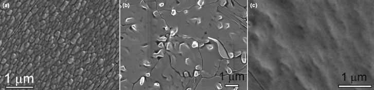
图18 MOCVD以VO(hfa)2/H2O为反应物制备的VO2薄膜及退火后的SEM照片[111]
Fig. 18 SEM images of VO2 films deposited by MOCVD using VO(hfa)2/H2O[111] (a) As-deposited VO2 film at 390 ℃; (b, c) VO2 films after annealed at (b) 575 and (c) 600 ℃ for 60 min

图19 ALD反应流程图[113]
Fig. 19 Schematic of ALD cycle[113] (a) Precursor A reacts with the substrate; (b) Excess precursor A and reaction byproducts are purged from the chamber; (c) Precursor B is pulsed into the chamber and reacts with the surface; (d) Excess precursor B and reaction products are purged from the chamber
| Vanadium precursor | Evaporator temperature/℃ | Oxidant | Substrate temperature/℃ | Annealing conditions | τc of VO2/℃ | Ref. |
|---|---|---|---|---|---|---|
| VO(acac)2 | 150 | O2 | 400-475 | - | 66-70 | [ |
| VO(acac)2 | - | O2 | 400-450 | 550-850 ℃ for 3 min | - | [ |
| VO(OC3H7)3 | RT | H2O | 60-90 | Ar plasma-annealing at 550 ℃ in vacuum | 68 | [ |
| TEMAV | 105 | O3 | 150 | 450 ℃ in He/O2 | 68 | [ |
| TEMAV | 105 | O3 | 150 | 2 h at 585 ℃ in 1.333×10⁻³ Pa O2 | 68 | [ |
| TEMAV | 105 | H2O | 150 | 450 ℃ in O2/Ar (13.33 Pa) | 70.1 | [ |
| TDMAV | RT | H2O/O3 | 50-200 | 550-800 ℃ in N2 for 2 h | - | [ |
| TDMAV | 60 | H2O | 150-200 | 475 ℃ in Ar for 100 min | 72 | [ |
| VCl4 | - | H2O | 350 | ≥500 ℃ in 90% N2/10% H2 for 60 min | 68 | [ |
表4 ALD制备VO2薄膜的工艺条件
Table 4 Summary of the ALD parameters used for the growth of VOx thin films
| Vanadium precursor | Evaporator temperature/℃ | Oxidant | Substrate temperature/℃ | Annealing conditions | τc of VO2/℃ | Ref. |
|---|---|---|---|---|---|---|
| VO(acac)2 | 150 | O2 | 400-475 | - | 66-70 | [ |
| VO(acac)2 | - | O2 | 400-450 | 550-850 ℃ for 3 min | - | [ |
| VO(OC3H7)3 | RT | H2O | 60-90 | Ar plasma-annealing at 550 ℃ in vacuum | 68 | [ |
| TEMAV | 105 | O3 | 150 | 450 ℃ in He/O2 | 68 | [ |
| TEMAV | 105 | O3 | 150 | 2 h at 585 ℃ in 1.333×10⁻³ Pa O2 | 68 | [ |
| TEMAV | 105 | H2O | 150 | 450 ℃ in O2/Ar (13.33 Pa) | 70.1 | [ |
| TDMAV | RT | H2O/O3 | 50-200 | 550-800 ℃ in N2 for 2 h | - | [ |
| TDMAV | 60 | H2O | 150-200 | 475 ℃ in Ar for 100 min | 72 | [ |
| VCl4 | - | H2O | 350 | ≥500 ℃ in 90% N2/10% H2 for 60 min | 68 | [ |

图20 ALD制备的氧化钒薄膜经过不同温度退火后的SEM照片[121]
Fig. 20 SEM images of ALD VO2 films annealed at different temperatures[121] (a) 550 ℃; (b) 700 ℃; (c) 850 ℃
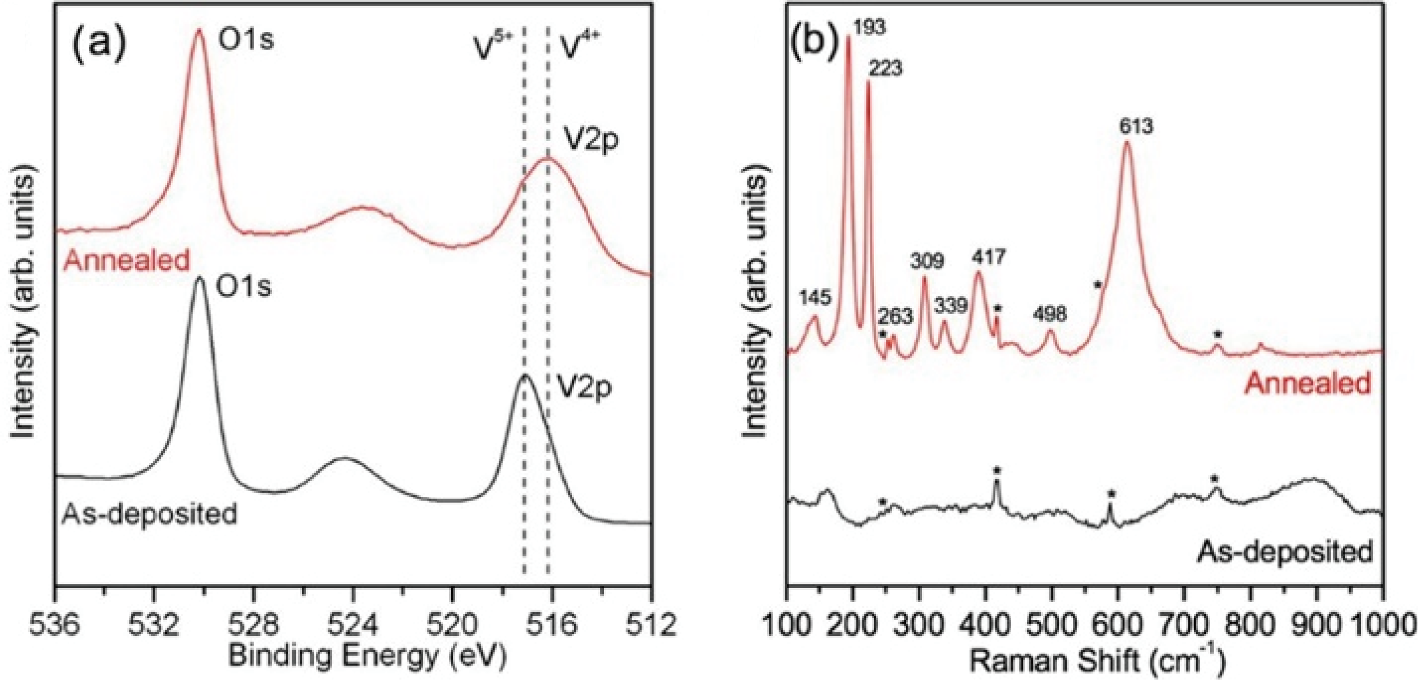
图21 ALD以TEMAV/O3为反应物制得的氧化钒薄膜(衬底为c-Al2O3)的XPS图谱[123]
Fig. 21 XPS spectra of ALD VO2 films using TEMAV/O3 as reactants on c-Al2O3[123] (a) XPS spectra of as-deposited (black) and annealed (red) VO2 films; (b) Raman spectra of as-deposited (black) and annealed (red) VO2 films

图22 ALD以TEMAV/H2O为反应物制得的VO2薄膜经退火后的SEM和AFM照片[133]
Fig. 22 SEM and AFM images of annealed H2O-based ALD VO2 films [133] (a) 28 nm; (b) 8 nm; (c) 4 nm

图23 单脉冲和多脉冲两种模式的ALD方法制备VO2薄膜[80]
Fig. 23 Schematic of SP and MP modes employed in the ALD process[80] (a) Typical sequence of the SP and MP modes of the ALD process; (b) Resistivity as a function of temperature and its derivative for the annealed VO2 thickness indicating the transition temperatures during heating and cooling cycle for depositions in SP and MP modes

图24 ALD以TDMAV/H2O为反应物在50 ℃下制备的VOx薄膜[119]
Fig. 24 ALD VOx films deposited with TDMAV/H2O at 50 ℃[119] (a) XRD patterns of VOx film before and after 2 h annealing at 800 ℃ under N2; (b) SEM images of as-deposited and annealed VOx films
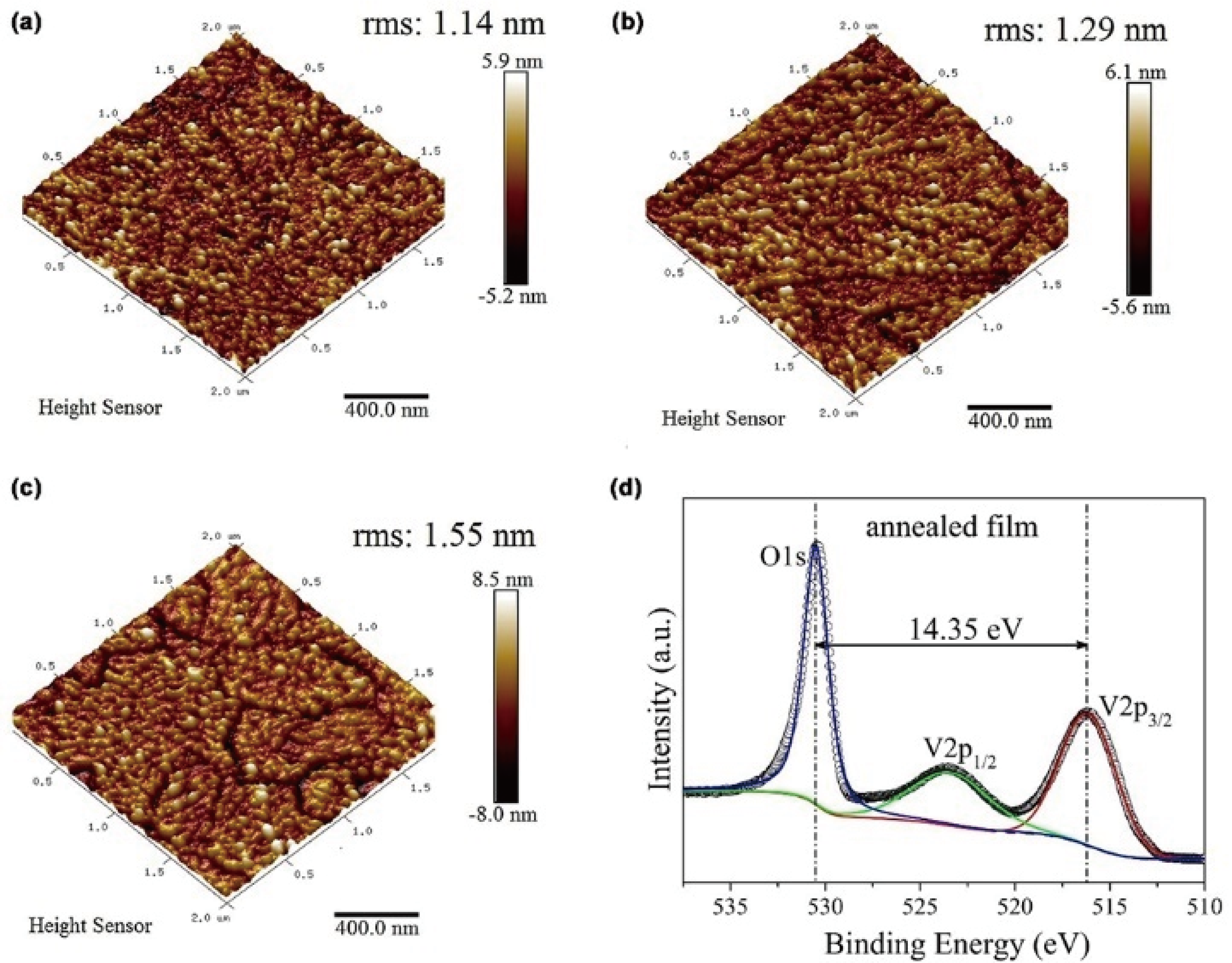
图25 ALD以TDMAV/H2O为反应物在150~200 ℃制备的VOx薄膜(在475 ℃氩气中退火100 min)[124]
Fig. 25 ALD VO2 films deposited from TDMAV/H2O at 150-200 ℃ and annealed at 475 ℃ for 100 min in Ar[124] (a-c) AFM images of VO2 films deposited at (a) 150, (b) 175 and (c) 200 ℃; (d) V2p XPS spectrum for the annealed VO2 film deposited at 200 ℃
图26 ALD以VCl4/H2O为反应物制得的VO2薄膜(在500和550 ℃退火)[125]
Fig. 26 ALD VO2 films deposited from VCl4/H2O and subsequently annealed at 500 and 550 ℃[125] (a) Raman spectra of as-deposited sample (black) and annealed samples at 500 (blue) and 550 ℃ (red); (b) XRD patterns of as-deposited and annealed VO2 films

图27 PECVD成膜的反应过程示意图[145]
Fig. 27 Schematic representation of the PECVD reaction process[145]

图28 RF-PECVD反应装置示意图[151]
Fig. 28 Schematic diagram of RF-PECVD system[151]

图29 WxV1-xO2d 晶体结构示意图[158]
Fig. 29 Crystalline structures of the WxV1-xO2[158] (a) Crystal structure relationship diagram of R and M1 phases; (b) Schematic diagram of local rutile structure around W dopant
| Vanadium precursor | Oxygen source | Dopant precursor | CVD process | Substrate/ temperature/℃ | Doping level/% (in atomic) | τc of VO2/℃ | Ref. |
|---|---|---|---|---|---|---|---|
| VOCl3 | H2O | WCl6 | APCVD | Glass/500-650 ℃ | 1.9 | 29 | [ |
| VCl4 | H2O | W(OC2H5)6 | APCVD | Glass/500-600 ℃ | 0.3 | 50 | [ |
| VCl4 | H2O | WCl6 | APCVD | Glass/550 ℃ | 0.12-1.75 | 55.0-5.5 | [ |
| VO(acac)2 | 2O2/98N2 | WCl6 | APCVD | Glass/525 ℃ | 0.5 | 55 | [ |
| VO(acac)2 | O2 | W(OC2H5)5 | MOCVD | Glass/450 ℃ | 2 | 35 | [ |
| VO(acac)2 | - | W(OC2H5)5 | AACVD | Glass/550 ℃ | 0.175-1.98 | 47-28 | [ |
| TEMAV | O2 | W(CO)6 | ALD | Si/200 ℃ | 1.63 | 32 | [ |
表5 CVD方法制备W掺杂VO2薄膜的工艺条件
Table 5 Summary of the CVD conditions for the synthesis of W-doped VO2 thin films
| Vanadium precursor | Oxygen source | Dopant precursor | CVD process | Substrate/ temperature/℃ | Doping level/% (in atomic) | τc of VO2/℃ | Ref. |
|---|---|---|---|---|---|---|---|
| VOCl3 | H2O | WCl6 | APCVD | Glass/500-650 ℃ | 1.9 | 29 | [ |
| VCl4 | H2O | W(OC2H5)6 | APCVD | Glass/500-600 ℃ | 0.3 | 50 | [ |
| VCl4 | H2O | WCl6 | APCVD | Glass/550 ℃ | 0.12-1.75 | 55.0-5.5 | [ |
| VO(acac)2 | 2O2/98N2 | WCl6 | APCVD | Glass/525 ℃ | 0.5 | 55 | [ |
| VO(acac)2 | O2 | W(OC2H5)5 | MOCVD | Glass/450 ℃ | 2 | 35 | [ |
| VO(acac)2 | - | W(OC2H5)5 | AACVD | Glass/550 ℃ | 0.175-1.98 | 47-28 | [ |
| TEMAV | O2 | W(CO)6 | ALD | Si/200 ℃ | 1.63 | 32 | [ |
| Dopant (s), (in atom) | τc | ΔTsol | Tlum/% | Ref. |
|---|---|---|---|---|
| W6+/0.6% | ~21.6 ℃/% | 11.4% | 50.8 | [ |
| Mo6+ | ~5 ℃/% | - | - | [ |
| Nb5+/10% | 52.2 ℃ | - | - | [ |
| Ta5+/4% | 24.8 ℃ | 6.8% | 47.1 | [ |
| Zr4+/9.8% | 64.3 ℃ | 14.1% | 60.4 | [ |
| Mg2+/7% | ~3 ℃/% | 4.8% | 51 | [ |
| Co2+/10% | 44 ℃ | 3% | 79 | [ |
| Tb3+/2% | 65 ℃ | 8.3% | 54 | [ |
| La3+/4% | ~1.1 ℃/% | 10.3 | 50.1 | [ |
| Eu3+/4% | ~6.5 ℃/% | 6.7% | 54 | [ |
| Si4+/3% | 63.1 ℃ | 13.9% | 54.7 | [ |
| Fe3+/Mg2+ | 38.2 ℃ | 12.8% | 42.1 | [ |
| Mg2+/W6+ | 35 ℃ | 4.3% | 81.3 | [ |
| Tb3+/W6+ | 40.8 ℃ | 6.3% | 40 | [ |
| Zr3+/W6+ | 28.6 ℃ | 4.9% | 48.6 | [ |
表6 部分掺杂元素对氧化钒薄膜热致变色性能的影响
Table 6 Effect of dopants on the thermochromic performance of VO2 thin films
| Dopant (s), (in atom) | τc | ΔTsol | Tlum/% | Ref. |
|---|---|---|---|---|
| W6+/0.6% | ~21.6 ℃/% | 11.4% | 50.8 | [ |
| Mo6+ | ~5 ℃/% | - | - | [ |
| Nb5+/10% | 52.2 ℃ | - | - | [ |
| Ta5+/4% | 24.8 ℃ | 6.8% | 47.1 | [ |
| Zr4+/9.8% | 64.3 ℃ | 14.1% | 60.4 | [ |
| Mg2+/7% | ~3 ℃/% | 4.8% | 51 | [ |
| Co2+/10% | 44 ℃ | 3% | 79 | [ |
| Tb3+/2% | 65 ℃ | 8.3% | 54 | [ |
| La3+/4% | ~1.1 ℃/% | 10.3 | 50.1 | [ |
| Eu3+/4% | ~6.5 ℃/% | 6.7% | 54 | [ |
| Si4+/3% | 63.1 ℃ | 13.9% | 54.7 | [ |
| Fe3+/Mg2+ | 38.2 ℃ | 12.8% | 42.1 | [ |
| Mg2+/W6+ | 35 ℃ | 4.3% | 81.3 | [ |
| Tb3+/W6+ | 40.8 ℃ | 6.3% | 40 | [ |
| Zr3+/W6+ | 28.6 ℃ | 4.9% | 48.6 | [ |
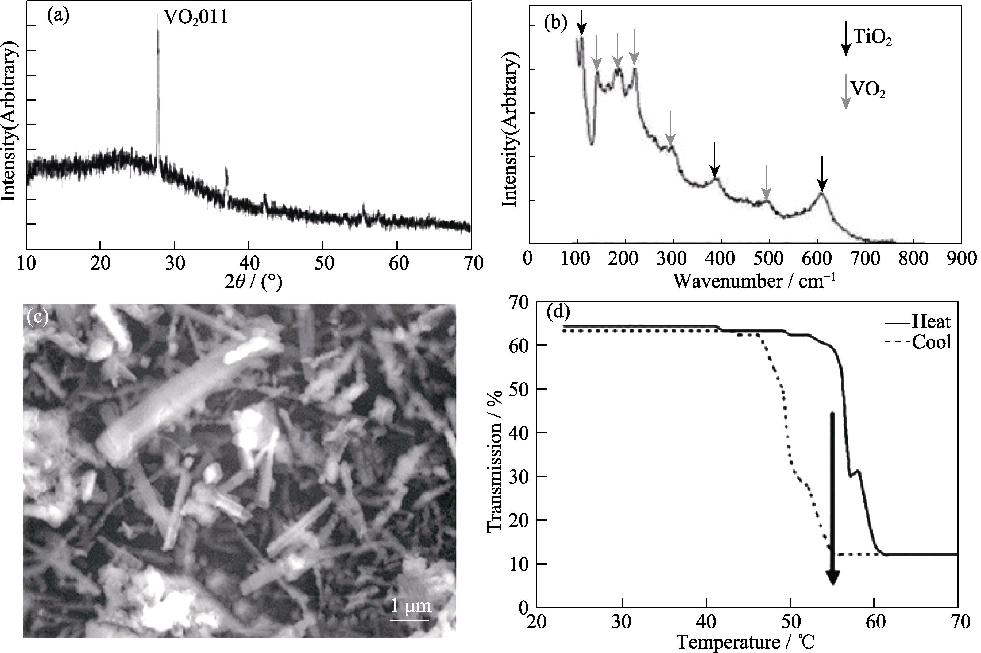
图30 APCVD以VOCl3/TTIP/H2O为反应物在650 ℃下得到VO2/TiO2复合薄膜表征[183]
Fig. 30 Characterization of VO2/TiO2 film formed by the APCVD reaction of VOCl3/TTIP/H2O at 650 ℃[183] (a) XRD pattern; (b) Raman spectrum; (c) SEM image; (d) Variable temperature transmission plot at 2.5 μm
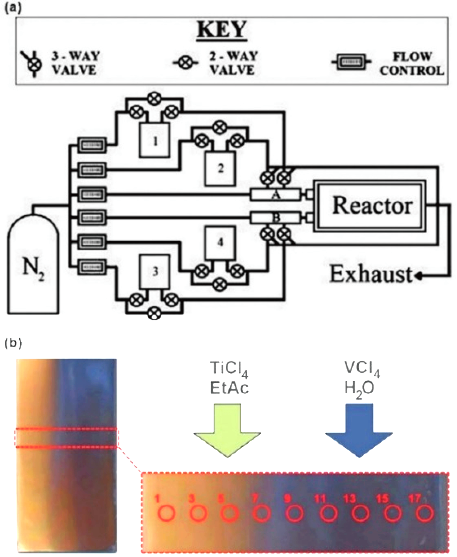
图31 组合APCVD制备VO2/TiO2复合薄膜[184]
Fig. 31 Combinatorial APCVD for the synthesis of VO2/TiO2 composite film[184] (a) Schematic of the APCVD apparatus; (b) Picture of the entire graded VO2/TiO2 composite film formed

图32 在VO2薄膜上应用折射率可调减反层的效果图[191]
Fig. 32 Schematic illustrating the concept of the RI-tunable ARC applied on the VO2 substrate[191]
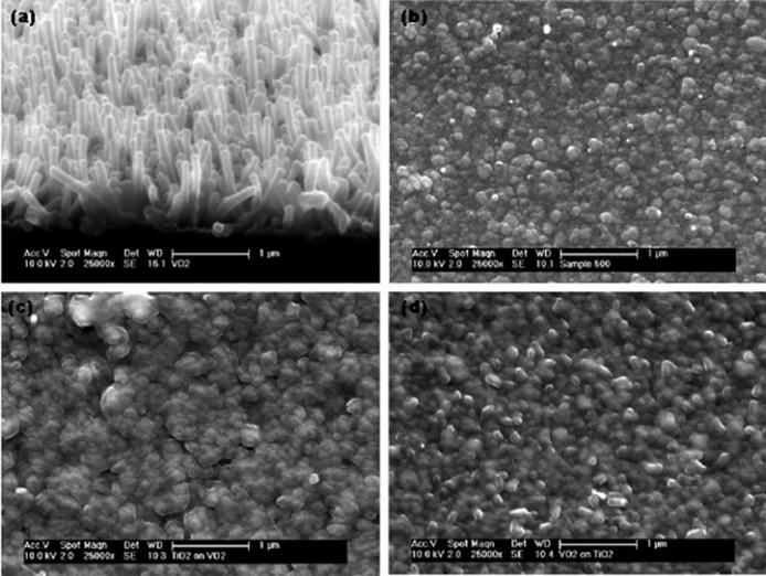
图33 APCVD制备的单层和双层薄膜的SEM照片[193]
Fig. 33 SEM images of the monolayer and multilayer samples prepared by APCVD[193] (a) VO2 film; (b) TiO2 film; (c) Multilayer of TiO2 over VO2; (d) Multilayer of VO2 over TiO2
| Layer | Precursor | Bubbler temperature /℃ | N2 flow rate /(L·min-1) | Thickness /nm |
|---|---|---|---|---|
| VO2 | VCl4/C4H8O4 | 80/40 | 0.7/0.2 | ~300 |
| SiO2 | SiC8H20O4/C4H8O4 | 130/40 | 0.7/0.2 | ~1300 |
| TiO2 | TiCl4/C4H8O4 | 75/40 | 0.6/0.6 | ~100 |
表7 APCVD制备VO2/SiO2/TiO2三层薄膜的工艺参数[195]
Table 7 APCVD conditions of the VO2/SiO2/TiO2 films[195]
| Layer | Precursor | Bubbler temperature /℃ | N2 flow rate /(L·min-1) | Thickness /nm |
|---|---|---|---|---|
| VO2 | VCl4/C4H8O4 | 80/40 | 0.7/0.2 | ~300 |
| SiO2 | SiC8H20O4/C4H8O4 | 130/40 | 0.7/0.2 | ~1300 |
| TiO2 | TiCl4/C4H8O4 | 75/40 | 0.6/0.6 | ~100 |

图34 APCVD制备的VO2/SiO2/TiO2三层薄膜的SEM照片[195]
Fig. 34 SEM images of multi-layered VO2/SiO2/TiO2 films using APCVD[195] (a) Typical VO2 coating on glass; (b) Porous structure of the SiO2 interlayer, as deposited on VO2 coating; (c) Typical surface morphology of the TiO2 layer in the VO2/SiO2/TiO2 system; (d) Side-on SEM image of VO2/SiO2/TiO2 film
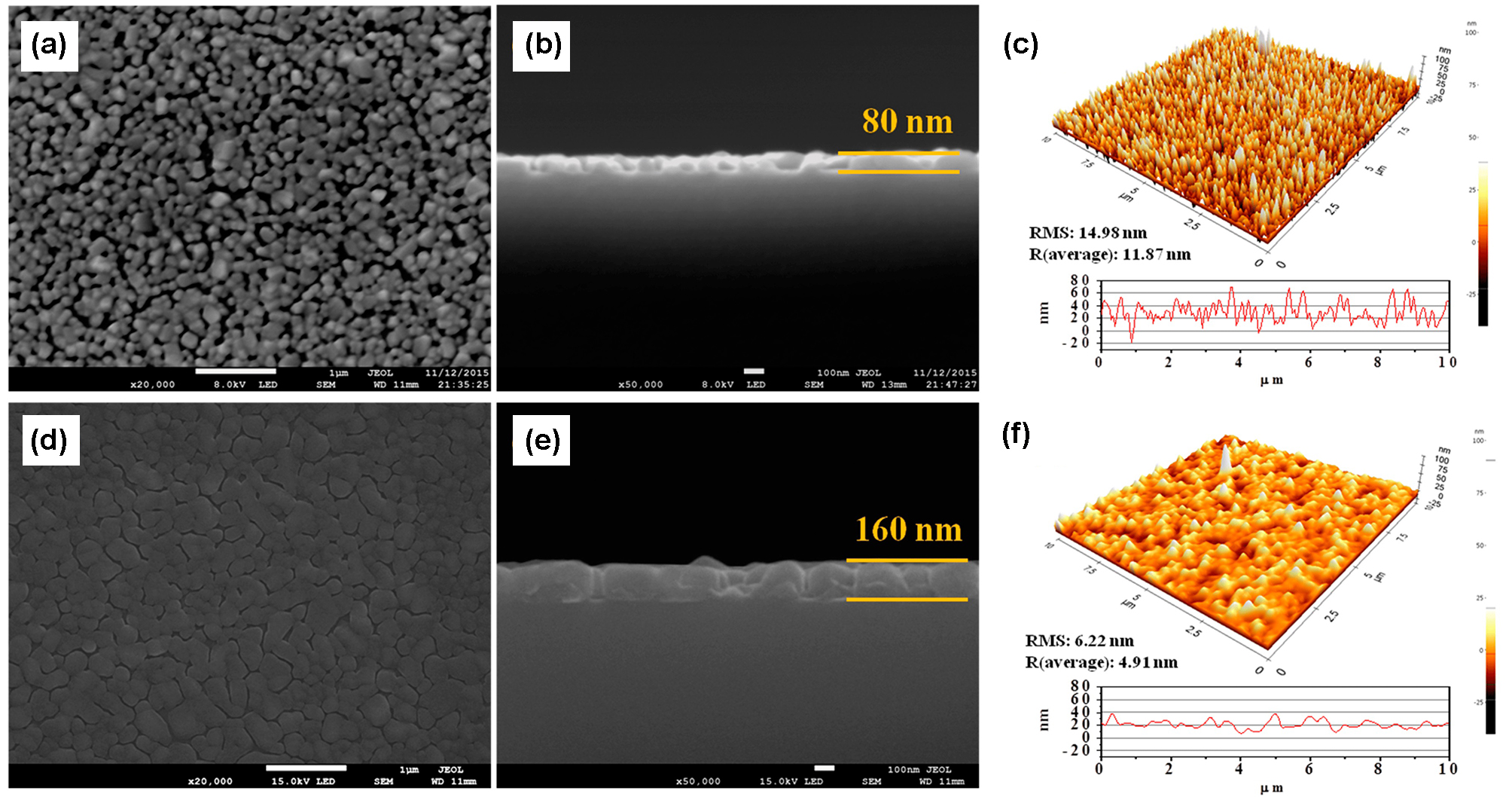
图35 VO2薄膜和SiO2/VO2双层薄膜的SEM和AFM照片[196]
Fig. 35 SEM and AFM images of VO2 and SiO2/VO2 thin films[196] (a, b) SEM and (c) AFM images of the pristine VO2 thin film; (d, e) SEM and (f) AFM images of SiO2/VO2 thin film
| [1] |
BERARDI U. A cross-country comparison of the building energy consumptions and their trends. Resources, Conservation and Recycling, 2017, 123: 230.
DOI URL |
| [2] |
DEFOREST N, SHEHABI A, SELKOWITZ S, et al. A comparative energy analysis of three electrochromic glazing technologies in commercial and residential buildings. Applied Energy, 2017, 192: 95.
DOI URL |
| [3] |
KE Y, ZHOU C, ZHOU Y, et al. Emerging thermal-responsive materials and integrated techniques targeting the energy-efficient smart window application. Advanced Functional Materials, 2018, 28(22): 1800113.
DOI URL |
| [4] |
SVENSSON J S E M, GRANQVIST C G. Electrochromic coatings for “smart windows”. Solar Energy Materials, 1985, 12(6): 391.
DOI URL |
| [5] |
WANG Y, RUNNERSTROM E L, MILLIRON D J. Switchable materials for smart windows. Annual Review of Chemical and Biomolecular Engineering, 2016, 7(1): 283.
DOI PMID |
| [6] |
KE Y, CHEN J, LIN G, et al. Smart windows: electro-, thermo-, mechano-, photochromics, and beyond. Advanced Energy Materials, 2019, 9(39): 1902066.
DOI URL |
| [7] |
WARWICK M E A, BINIONS R. Advances in thermochromic vanadium dioxide films. Journal of Materials Chemistry A, 2014, 2(10): 3275.
DOI URL |
| [8] |
CUI Y, KE Y, LIU C, et al. Thermochromic VO2 for energy-efficient smart windows. Joule, 2018, 2(9): 1707.
DOI URL |
| [9] |
MATAMURA Y, IKENOUE T, MIYAKE M, et al. Mist CVD of vanadium dioxide thin films with excellent thermochromic properties using a water-based precursor solution. Solar Energy Materials and Solar Cells, 2021, 230: 111287.
DOI URL |
| [10] |
SJOBERG S G. Nils Gabriel Sefstrom and the discovery of vanadium. Journal of Chemical Education, 1951, 28(6): 294.
DOI URL |
| [11] |
MORIN F J. Oxides which show a metal-to-insulator transition at the neel temperature. Physical Review Letters, 1959, 3(1): 34.
DOI URL |
| [12] |
GOODENOUGH J B. The two components of the crystallographic transition in VO2. Journal of Solid State Chemistry, 1971, 3(4): 490.
DOI URL |
| [13] |
WHITTAKER L, PATRIDGE C J, BANERJEE S. Microscopic and nanoscale perspective of the metal-insulator phase transitions of VO2: some new twists to an old tale. The Journal of Physical Chemistry Letters, 2011, 2(7): 745.
DOI URL |
| [14] |
AETUKURI N B, GRAY A X, DROUARD M, et al. Control of the metal-insulator transition in vanadium dioxide by modifying orbital occupancy. Nature Physics, 2013, 9(10): 661.
DOI |
| [15] |
BABULANAM S M, ERIKSSON T S, NIKLASSON G A, et al. Thermochromic VO2 films for energy-efficient windows. Solar Energy Materials, 1987, 16(5): 347.
DOI URL |
| [16] |
BARIMAH E K, BOONTAN A, STEENSON D P, et al. Infrared optical properties modulation of VO2 thin film fabricated by ultrafast pulsed laser deposition for thermochromic smart window applications. Scientific Reports, 2022, 12: 11421.
DOI |
| [17] |
CHANG T, CAO X, DEDON L R, et al. Optical design and stability study for ultrahigh-performance and long-lived vanadium dioxide-based thermochromic coatings. Nano Energy, 2018, 44: 256.
DOI URL |
| [18] |
LIU K, LEE S, YANG S, et al. Recent progresses on physics and applications of vanadium dioxide. Materials Today, 2018, 21(8): 875.
DOI URL |
| [19] | CHEN S, WANG Z, REN H, et al. Gate-controlled VO2 phase transition for high-performance smart windows. Science Advances, 2019, 5(3): 6815. |
| [20] |
VU T D, CHEN Z, ZENG X, et al. Physical vapour deposition of vanadium dioxide for thermochromic smart window applications. Journal of Materials Chemistry C, 2019, 7(8): 2121.
DOI URL |
| [21] |
YAO L, QU Z, PANG Z, et al. Three-layered hollow nanospheres based coatings with ultrahigh-performance of energy-saving, antireflection, and self-cleaning for smart windows. Small, 2018, 14(34): 1801661.
DOI URL |
| [22] |
ABURAS M, SOEBARTO V, WILLIAMSON T, et al. Thermochromic smart window technologies for building application: a review. Applied Energy, 2019, 255: 113522.
DOI URL |
| [23] |
KE Y, YIN Y, ZHANG Q, et al. Adaptive thermochromic windows from active plasmonic elastomers. Joule, 2019, 3(3): 858.
DOI |
| [24] |
CAO X, CHANG T, SHAO Z, et al. Challenges and opportunities toward real application of VO2-based smart glazing. Matter, 2020, 2(4): 862.
DOI URL |
| [25] |
ZENG W, CHEN N, XIE W. Research progress on the preparation methods for VO2 nanoparticles and their application in smart windows. CrystEngComm, 2020, 22(5): 851.
DOI URL |
| [26] |
CHEN Z, TANG Y, JI A, et al. Large-scale preparation of durable VO2 nanocomposite coatings. ACS Applied Nano Materials, 2021, 4(4): 4048.
DOI URL |
| [27] |
WANG S, JIANG T, MENG Y, et al. Scalable thermochromic smart windows with passive radiative cooling regulation. Science, 2021, 374(6574): 1501.
DOI PMID |
| [28] | CAO C, HU B, TU G, et al. Sputtering flexible VO2 films for effective thermal modulation. ACS Applied Materials & Interfaces, 2022, 14(24): 28105. |
| [29] |
SUN K, WHEELER C, HILLIER J A, et al. Room temperature phase transition of W-doped VO2 by atomic layer deposition on 200 mm Si wafers and flexible substrates. Advanced Optical Materials, 2022, 10(23): 2201326.
DOI URL |
| [30] |
VU T D, XIE H, WANG S, et al. Durable vanadium dioxide with 33-year service life for smart windows applications. Materials Today Energy, 2022, 26: 100978.
DOI URL |
| [31] | TANG K, DONG K, LI J, et al. Temperature-adaptive radiative coating for all-season household thermal regulation. 2021, 374(6574): 1504. |
| [32] |
SHEN N, CHEN S, HUANG R, et al. Vanadium dioxide for thermochromic smart windows in ambient conditions. Materials Today Energy, 2021, 21: 100827.
DOI URL |
| [33] |
KIM J, PAIK T. Recent advances in fabrication of flexible, thermochromic vanadium dioxide films for smart windows. Nanomaterials (Basel), 2021, 11(10): 2674.
DOI URL |
| [34] |
LI X, CAO C, LIU C, et al. Self-rolling of vanadium dioxide nanomembranes for enhanced multi-level solar modulation. Nature Communications, 2022, 13: 7819.
DOI PMID |
| [35] |
LI S Y, NIKLASSON G A, GRANQVIST C G. Thermochromic fenestration with VO2-based materials: three challenges and how they can be met. Thin Solid Films, 2012, 520(10): 3823.
DOI URL |
| [36] |
WANG S, OWUSU K A, MAI L, et al. Vanadium dioxide for energy conservation and energy storage applications: synthesis and performance improvement. Applied Energy, 2018, 211: 200.
DOI URL |
| [37] |
SHAO Z, CAO X, LUO H, et al. Recent progress in the phase-transition mechanism and modulation of vanadium dioxide materials. NPG Asia Materials, 2018, 10(7): 581.
DOI |
| [38] |
HU P, HU P, VU T D, et al. Vanadium oxide: phase diagrams, structures, synthesis, and applications. Chemical Reviews, 2023, 123(8): 4353.
DOI URL |
| [39] |
KOSUGE K. The phase diagram and phase transition of the V2O3-V2O5 system. Journal of Physics and Chemistry of Solids, 1967, 28(8): 1613.
DOI URL |
| [40] |
WRIEDT H A. The O-V (oxygen-vanadium) system. Bulletin of Alloy Phase Diagrams, 1989, 10(3): 271.
DOI URL |
| [41] |
CHOI Y, JUNG Y, KIM H. Low-temperature deposition of thermochromic VO2 thin films on glass substrates. Thin Solid Films, 2016, 615: 437.
DOI URL |
| [42] |
ZHANG D P, ZHU M D, LIU Y, et al. High performance VO2 thin films growth by DC magnetron sputtering at low temperature for smart energy efficient window application. Journal of Alloys and Compounds, 2016, 659: 198.
DOI URL |
| [43] |
AIJAZ A, JI Y X, MONTERO J, et al. Low-temperature synthesis of thermochromic vanadium dioxide thin films by reactive high power impulse magnetron sputtering. Solar Energy Materials and Solar Cells, 2016, 149: 137.
DOI URL |
| [44] |
TAHA M, WALIA S, AHMED T, et al. Insulator-metal transition in substrate-independent VO2 thin film for phase-change devices. Scientific Reports, 2017, 7: 17899.
DOI |
| [45] |
VU T D, LIU S, ZENG X, et al. High-power impulse magnetron sputtering deposition of high crystallinity vanadium dioxide for thermochromic smart windows applications. Ceramics International, 2020, 46(6): 8145.
DOI URL |
| [46] |
ZHU M, WANG H, WANG B, et al. New route for modification of thermochromic properties of vanadium dioxide films via high-energy X-ray irradiation. Ceramics International, 2019, 45(2, Part A): 1661.
DOI URL |
| [47] |
LIU B, GONG M, ZHANG J, et al. Comparative study of the metal insulator transition of a VO2 film with simultaneous infrared thermography and electric measurements. AIP Advances, 2021, 11(3): 035026.
DOI URL |
| [48] |
CASE F C. Low temperature deposition of VO2 thin films. Journal of Vacuum Science & Technology A, 1990, 8(3): 1395.
DOI URL |
| [49] |
LEE M H, KIM M G. RTA and stoichiometry effect on the thermochromism of VO2 thin films. Thin Solid Films, 1996, 286(1): 219.
DOI URL |
| [50] |
THéRY V, BOULLE A, CRUNTEANU A, et al. Structural and electrical properties of large area epitaxial VO2 films grown by electron beam evaporation. Journal of Applied Physics, 2017, 121(5): 055303.
DOI URL |
| [51] |
MANOUSOU D K, GARDELIS S, CALAMIOTOU M, et al. VO2 thin films fabricated by reduction of thermal evaporated V2O5 under N2 flow. Materials Letters, 2021, 299: 130086.
DOI URL |
| [52] |
GUO X, TAN Y, HU Y, et al. High quality VO2 thin films synthesized from V2O5 powder for sensitive near-infrared detection. Scientific Reports, 2021, 11: 21749.
DOI |
| [53] |
PóSA L, MOLNÁR G, KALAS B, et al. A rational fabrication method for low switching-temperature VO2. Nanomaterials (Basel), 2021, 11(1): 212.
DOI URL |
| [54] |
KIM D H, KWOK H S. Pulsed laser deposition of VO2 thin films. Applied Physics Letters, 1994, 65(25): 3188.
DOI URL |
| [55] |
ZHU P R, YAMAMOTO S, MIYASHITA A, et al. Pulsed laser deposition of VO2 single crystal thin films on sapphire substrates. Chinese Physics Letters, 1998, 15(12): 904.
DOI URL |
| [56] |
LIU H, VASQUEZ O, SANTIAGO V R, et al. Novel pulsed-laser-deposition—VO2 thin films for ultrafast applications. Journal of Electronic Materials, 2005, 34(5): 491.
DOI URL |
| [57] |
FU D, LIU K, TAO T, et al. Comprehensive study of the metal-insulator transition in pulsed laser deposited epitaxial VO2 thin films. Journal of Applied Physics, 2013, 113(4): 043707.
DOI URL |
| [58] |
MATHEVULA L, NGOM B D, KOTSEDI L, et al. Thermochromic VO2 on zinnwaldite mica by pulsed laser deposition. Applied Surface Science, 2014, 314: 476.
DOI URL |
| [59] |
KUMI-BARIMAH E, ANAGNOSTOU D E, JOSE G. Phase changeable vanadium dioxide (VO2) thin films grown from vanadium pentoxide (V2O5) using femtosecond pulsed laser deposition. AIP Advances, 2020, 10(6): 065225.
DOI URL |
| [60] |
BUKHARI S A, KUMAR S, KUMAR P, et al. The effect of oxygen flow rate on metal-insulator transition (MIT) characteristics of vanadium dioxide (VO2) thin films by pulsed laser deposition (PLD). Applied Surface Science, 2020, 529: 146995.
DOI URL |
| [61] |
YIN D, XU N, ZHANG J, et al. High quality vanadium dioxide films prepared by an inorganic Sol-Gel method. Materials Research Bulletin, 1996, 31(3): 335.
DOI URL |
| [62] |
LU S, HOU L, GAN F. Structure and optical property changes of sol-gel derived VO2 thin films. Advanced Materials, 1997, 9(3): 244.
DOI URL |
| [63] |
LU S, HOU L, GAN F. Surface analysis and phase transition of gel-derived VO2 thin films. Thin Solid Films, 1999, 353(1): 40.
DOI URL |
| [64] |
YAN J, HUANG W, ZHANG Y, et al. Characterization of preferred orientated vanadium dioxide film on muscovite (001) substrate. Physica Status Solidi (a), 2008, 205(10): 2409.
DOI URL |
| [65] |
LIU D, CHENG H, ZHENG W, et al. Infrared thermochromic properties of VO2 thin films prepared through aqueous Sol-Gel process. Journal of Wuhan University of Technology-Mater. Sci. Ed., 2012, 27(5): 861.
DOI URL |
| [66] |
WU Y F, FAN L L, CHEN S M, et al. Spectroscopic analysis of phase constitution of high quality VO2 thin film prepared by facile Sol-Gel method. AIP Advances, 2013, 3(4): 042132.
DOI URL |
| [67] | KANG L, GAO Y, LUO H. A novel solution process for the synthesis of VO2 thin films with excellent thermochromic properties. ACS Applied Materials & Interfaces, 2009, 1(10): 2211. |
| [68] | KANG L, GAO Y, LUO H, et al. Nanoporous thermochromic VO2 films with low optical constants, enhanced luminous transmittance and thermochromic properties. ACS Applied Materials & Interfaces, 2011, 3(2): 135. |
| [69] |
YUE F, HUANG W, SHI Q, et al. Phase transition properties of vanadium oxide films deposited by polymer-assisted deposition. Journal of Sol-Gel Science and Technology, 2014, 72(3): 565.
DOI URL |
| [70] |
BRECKENFELD E, KIM H, GORZKOWSKI E P, et al. Laser-processing of VO2 thin films synthesized by polymer-assisted-deposition. Applied Surface Science, 2017, 397: 152.
DOI URL |
| [71] |
DEVTHADE V, LEE S. Synthesis of vanadium dioxide thin films and nanostructures. Journal of Applied Physics, 2020, 128(23): 231101.
DOI URL |
| [72] |
SUN L, YUAN G, GAO L, et al. Chemical vapour deposition. Nature Reviews Methods Primers, 2021, 1(1): 5.
DOI |
| [73] |
WARWICK M E A, BINIONS R. Chemical vapour deposition of thermochromic vanadium dioxide thin films for energy efficient glazing. Journal of Solid State Chemistry, 2014, 214: 53.
DOI URL |
| [74] | DROSOS C, VERNARDOU D. Perspectives of energy materials grown by APCVD. Solar Energy Materials and Solar Cells, 2015, 140: 1. |
| [75] |
MARUYAMA T, IKUTA Y. Vanadium dioxide thin films prepared by chemical vapour deposition from vanadium(III) acetylacetonate. Journal of Materials Science, 1993, 28(18): 5073.
DOI URL |
| [76] |
LIM B S, RAHTU A, PARK J S, et al. Synthesis and characterization of volatile, thermally stable, reactive transition metal amidinates. Inorganic Chemistry, 2003, 42(24): 7951.
PMID |
| [77] |
PRASADAM V P, BAHLAWANE N, MATTELAER F, et al. Atomic layer deposition of vanadium oxides: process and application review. Materials Today Chemistry, 2019, 12: 396.
DOI URL |
| [78] |
WEIMER M S, KIM I S, GUO P, et al. Oxidation state discrimination in the atomic layer deposition of vanadium oxides. Chemistry of Materials, 2017, 29(15): 6238.
DOI URL |
| [79] |
PRASADAM V P, DEY B, BULOU S, et al. Study of VO2 thin film synthesis by atomic layer deposition. Materials Today Chemistry, 2019, 12: 332.
DOI URL |
| [80] |
NIANG K M, BAI G, ROBERTSON J. Influence of precursor dose and residence time on the growth rate and uniformity of vanadium dioxide thin films by atomic layer deposition. Journal of Vacuum Science & Technology A, 2020, 38(4): 042401.
DOI URL |
| [81] |
BAI G, NIANG K M, ROBERTSON J. Preparation of atomic layer deposited vanadium dioxide thin films using tetrakis (ethylmethylamino) vanadium as precursor. Journal of Vacuum Science & Technology A, 2020, 38(5): 052402.
DOI URL |
| [82] |
THOMAS T, BLACKMAN C S, PARKIN I P, et al. Atmospheric pressure chemical vapour deposition of vanadium arsenide thin films via the reaction of VCl4 or VOCl3 with tBuAsH2. Thin Solid Films, 2013, 537: 171.
DOI URL |
| [83] |
MALKEROVA I P, MAKAREVICH A M, ALIKHANYAN A S, et al. Volatility and thermal stability of vanadyl β-diketonate complexes. Russian Journal of Inorganic Chemistry, 2017, 62(6): 818.
DOI URL |
| [84] |
KANAI H, YOSHIKAWA T, SONE T, et al. Preparation and characterization of highly dispersed V2O5/SiO2 prepared by a CVD method. Reaction Kinetics and Catalysis Letters, 2002, 75(2): 213.
DOI URL |
| [85] |
BADOT J C. Atomic layer epitaxy of vanadium oxide thin films and electrochemical behavior in presence of lithium ions. Electrochemical and Solid-State Letters, 1999, 3(10): 485.
DOI URL |
| [86] |
MANNING T D, PARKIN I P, CLARK R J H, et al. Intelligent window coatings: atmospheric pressure chemical vapour deposition of vanadium oxides. Journal of Materials Chemistry, 2002, 12(10): 2936.
DOI URL |
| [87] |
DROSOS C, VERNARDOU D. Advancements, challenges and prospects of chemical vapour pressure at atmospheric pressure on vanadium dioxide structures. Materials, 2018, 11(3): 384.
DOI URL |
| [88] |
FIELD M N, PARKIN I P. Atmospheric pressure chemical vapour deposition of vanadium(V) oxide films on glass substrates from reactions of VOCl3 and VCl4 with water. Journal of Materials Chemistry, 2000, 10(8): 1863.
DOI URL |
| [89] |
MANNING T D, PARKIN I P. Vanadium(IV) oxide thin films on glass and silicon from the atmospheric pressure chemical vapour deposition reaction of VOCl3 and water. Polyhedron, 2004, 23(18): 3087.
DOI URL |
| [90] |
VERNARDOU D, PATERAKIS P, DROSOS H, et al. A study of the electrochemical performance of vanadium oxide thin films grown by atmospheric pressure chemical vapour deposition. Solar Energy Materials and Solar Cells, 2011, 95(10): 2842.
DOI URL |
| [91] |
MALARDE D, POWELL M J, QUESADA-CABRERA R, et al. Optimized atmospheric-pressure chemical vapor deposition thermochromic VO2 thin films for intelligent window applications. ACS Omega, 2017, 2(3): 1040.
DOI URL |
| [92] |
GASKELL J M, AFZAAL M, SHEEL D W, et al. Optimised atmospheric pressure CVD of monoclinic VO2 thin films with picosecond phase transition. Surface and Coatings Technology, 2016, 287: 160.
DOI URL |
| [93] |
VERNARDOU D, PEMBLE M E, SHEEL D W. The growth of thermochromic VO2 films on glass by atmospheric-pressure CVD: a comparative study of precursors, CVD methodology, and substrates. Chemical Vapor Deposition, 2006, 12(5): 263.
DOI URL |
| [94] |
VERNARDOU D, LOULOUDAKIS D, SPANAKIS E, et al. Thermochromic amorphous VO2 coatings grown by APCVD using a single-precursor. Solar Energy Materials and Solar Cells, 2014, 128: 36.
DOI URL |
| [95] |
VERNARDOU D, PEMBLE M E, SHEEL D W. In-situ Fourier transform infrared spectroscopy gas phase studies of vanadium (IV) oxide coating by atmospheric pressure chemical vapour deposition using vanadyl (IV) acetylacetonate. Thin Solid Films, 2008, 516(14): 4502.
DOI URL |
| [96] | VERNARDOU D, BEI A, LOULOUDAKIS D, et al. Oxygen source-oriented control of atmospheric pressure chemical vapor deposition of VO2 for capacitive applications. Journal of Electrochemical Science and Engineering, 2016, 6(2): 165. |
| [97] |
WARWICK M E A, RIDLEY I, BINIONS R. Thermochromic vanadium dioxide thin films prepared by electric field assisted atmospheric pressure chemical vapour deposition for intelligent glazing application and their energy demand reduction properties. Solar Energy Materials and Solar Cells, 2016, 157: 686.
DOI URL |
| [98] |
MATHUR S, RUEGAMER T, GROBELSEK I. Phase-selective CVD of vanadium oxide nanostructures. Chemical Vapor Deposition, 2007, 13(1): 42.
DOI URL |
| [99] |
PAPADIMITROPOULOS G, KOSTIS I, TRANTALIDIS S, et al. Investigation of structural, morphological and electrical properties of APCVD vanadium oxide thin films. Physica Status Solidi C, 2015, 12(7): 964.
DOI URL |
| [100] |
JIAMPRASERTBOON A, POWELL M J, DIXON S C, et al. Photocatalytic and electrically conductive transparent Cl-doped ZnO thin films via aerosol-assisted chemical vapour deposition. Journal of Materials Chemistry A, 2018, 6(26): 12682.
DOI URL |
| [101] |
PICCIRILLO C, BINIONS R, PARKIN I P. Synthesis and functional properties of vanadium oxides: V2O3, VO2, and V2O5 deposited on glass by aerosol-assisted CVD. Chemical Vapor Deposition, 2007, 13(4): 145.
DOI URL |
| [102] |
WARWICK M E A, BINIONS R. Thermochromic vanadium dioxide thin films from electric field assisted aerosol assisted chemical vapour deposition. Solar Energy Materials and Solar Cells, 2015, 143: 592.
DOI URL |
| [103] |
GUO B, CHEN L, SHI S, et al. Low temperature fabrication of thermochromic VO2 thin films by low-pressure chemical vapor deposition. RSC Advances, 2017, 7(18): 10798.
DOI URL |
| [104] |
WRIGHT P J, CROSBIE M J, LANE P A, et al. Metal organic chemical vapor deposition (MOCVD) of oxides and ferroelectric materials. Journal of Materials Science: Materials in Electronics, 2002, 13(11): 671.
DOI URL |
| [105] |
YAKOVKINA L V, MUTILIN S V, PRINZ V Y, et al. MOCVD growth and characterization of vanadium dioxide films. Journal of Materials Science, 2017, 52(7): 4061.
DOI URL |
| [106] |
SPANÒ S F, TORO R G, CONDORELLI G G, et al. Phase- selective route to V-O film formation: a systematic MOCVD study into the effects of deposition temperature on structure and morphology. Chemical Vapor Deposition, 2015, 21: 319.
DOI URL |
| [107] |
SAHANA M B, DHARMAPRAKASH M S, SHIVASHANKAR S A. Microstructure and properties of VO2 thin films deposited by MOCVD from vanadyl acetylacetonate. Journal of Materials Chemistry, 2002, 12(2): 333.
DOI URL |
| [108] |
VERNARDOU D, PEMBLE M E, SHEEL D W. Vanadium oxides prepared by liquid injection MOCVD using vanadyl acetylacetonate. Surface and Coatings Technology, 2004, 188-189: 250.
DOI URL |
| [109] |
RAJESWARAN B, UMARJI A M. Defect engineering of VO2 thin films synthesized by chemical vapor deposition. Materials Chemistry and Physics, 2020, 245: 122230.
DOI URL |
| [110] |
MAKAREVICH A M, SADYKOV I I, SHAROVAROV D I, et al. Chemical synthesis of high quality epitaxial vanadium dioxide films with sharp electrical and optical switch properties. Journal of Materials Chemistry C, 2015, 3(35): 9197.
DOI URL |
| [111] |
MAKAREVICH A M, SOBOL A G, SADYKOV I I, et al. Delicate tuning of epitaxial VO2 films for ultra-sharp electrical and intense IR optical switching properties. Journal of Alloys and Compounds, 2021, 853: 157214.
DOI URL |
| [112] |
LESKELä M, RITALA M. Atomic layer deposition (ALD): from precursors to thin film structures. Thin Solid Films, 2002, 409(1): 138.
DOI URL |
| [113] |
ASUNDI A S, RAIFORD J A, BENT S F. Opportunities for atomic layer deposition in emerging energy technologies. ACS Energy Letters, 2019, 4(4): 908.
DOI URL |
| [114] |
SUNTOLA T. Atomic layer epitaxy. Materials Science Reports, 1989, 4(5): 261.
DOI URL |
| [115] |
ØSTRENG E, NILSEN O, FJELLVÅG H. Optical properties of vanadium pentoxide deposited by ALD. The Journal of Physical Chemistry C, 2012, 116(36): 19444.
DOI URL |
| [116] |
ØSTRENG E, GANDRUD K B, HU Y, et al. High power nano- structured V2O5 thin film cathodes by atomic layer deposition. Journal of Materials Chemistry A, 2014, 2(36): 15044.
DOI URL |
| [117] |
CHEN X, POMERANTSEVA E, BANERJEE P, et al. Ozone-based atomic layer deposition of crystalline V2O5 films for high performance electrochemical energy storage. Chemistry of Materials, 2012, 24(7): 1255.
DOI URL |
| [118] |
BLANQUART T, NIINISTÖ J, GAVAGNIN M, et al. Atomic layer deposition and characterization of vanadium oxide thin films. RSC Advances, 2013, 3(4): 1179.
DOI URL |
| [119] |
WANG X, GUO Z, GAO Y, et al. Atomic layer deposition of vanadium oxide thin films from tetrakis(dimethylamino)vanadium precursor. Journal of Materials Research, 2017, 32(1): 37.
DOI URL |
| [120] | DAGUR P, MANE A U, SHIVASHANKAR S A. Thin films of VO2 on glass by atomic layer deposition: microstructure and electrical properties. Journal of Crystal Growth, 2005, 275(1): 1223. |
| [121] |
JUAN P C, LIN K C, CHO W H, et al. Atomic layer deposition of vanadium oxides using vanadyl acetylacetonate as the precursor. Thin Solid Films, 2021, 725: 138639.
DOI URL |
| [122] |
RAMPELBERG G, DEDUYTSCHE D, DE SCHUTTER B, et al. Crystallization and semiconductor-metal switching behavior of thin VO2 layers grown by atomic layer deposition. Thin Solid Films, 2014, 550: 59.
DOI URL |
| [123] |
KOZEN A C, JORESS H, CURRIE M, et al. Structural characterization of atomic layer deposited vanadium dioxide. The Journal of Physical Chemistry C, 2017, 121(35): 19341.
DOI URL |
| [124] |
LV X, CAO Y, YAN L, et al. Atomic layer deposition of VO2 films with tetrakis-dimethyl-amino vanadium (IV) as vanadium precursor. Applied Surface Science, 2017, 396: 214.
DOI URL |
| [125] |
GANESAN J P, DEV D, KRISHNAPRASAD A, et al. Semiconductor- to-metal transition in atomic layer deposition (ALD) of VO2 films using VCl4 and water. Applied Physics Letters, 2021, 118(26): 261902.
DOI URL |
| [126] |
KERÄNEN J, AUROUX A, EK-HÄRKÖNEN S, et al. Calorimetric measurements of the acidity of supported vanadium oxides prepared by ALE and impregnation. Thermochimica Acta, 2001, 379(1): 233.
DOI URL |
| [127] |
MUSSCHOOT J, DEDUYTSCHE D, POELMAN H, et al. Comparison of thermal and plasma-enhanced ALD/CVD of vanadium pentoxide. Journal of the Electrochemical Society, 2009, 156(7): P122.
DOI URL |
| [128] |
DAUBERT J S, LEWIS N P, GOTSCH H N, et al. Effect of meso- and micro-porosity in carbon electrodes on atomic layer deposition of pseudocapacitive V2O5 for high performance supercapacitors. Chemistry of Materials, 2015, 27(19): 6524.
DOI URL |
| [129] |
DAUBERT J S, WANG R, OVENTAL J S, et al. Intrinsic limitations of atomic layer deposition for pseudocapacitive metal oxides in porous electrochemical capacitor electrodes. Journal of Materials Chemistry A, 2017, 5(25): 13086.
DOI URL |
| [130] |
RAMPELBERG G, SCHAEKERS M, MARTENS K, et al. Semiconductor-metal transition in thin VO2 films grown by ozone based atomic layer deposition. Applied Physics Letters, 2011, 98(16): 162902.
DOI URL |
| [131] | ZHANG K, TANGIRALA M, NMINIBAPIEL D, et al. Synthesis of VO2 thin films by atomic layer deposition with TEMAV as precursor. ECS Transactions, 2013, 50(13): 175. |
| [132] |
PREMKUMAR P A, TOELLER M, RADU I P, et al. Process study and characterization of VO2 thin films synthesized by ALD using TEMAV and O3 precursors. ECS Journal of Solid State Science and Technology, 2012, 1(4): P169.
DOI URL |
| [133] |
PETER A P, MARTENS K, RAMPELBERG G, et al. Metal- insulator transition in ALD VO2 ultrathin films and nanoparticles: morphological control. Advanced Functional Materials, 2015, 25(5): 679.
DOI URL |
| [134] |
MATTELAER F, GERYL K, RAMPELBERG G, et al. Atomic layer deposition of vanadium oxides for thin-film lithium-ion battery applications. RSC Advances, 2016, 6(115): 114658.
DOI URL |
| [135] |
CURRIE M, MASTRO M A, WHEELER V D. Characterizing the tunable refractive index of vanadium dioxide. Optical Materials Express, 2017, 7(5): 1697.
DOI URL |
| [136] | CURRIE M, MASTRO M A, WHEELER V D. Atomic layer deposition of vanadium dioxide and a temperature-dependent optical model. Journal of Visualized Experiments, 2018, 135: 57103. |
| [137] |
GAO Y, SHAO Y, YAN L, et al. Efficient charge injection in organic field-effect transistors enabled by low-temperature atomic layer deposition of ultrathin VOx interlayer. Advanced Functional Materials, 2016, 26(25): 4456.
DOI URL |
| [138] |
SILVERSMIT G, DEPLA D, POELMAN H, et al. Determination of the V2p XPS binding energies for different vanadium oxidation states (V5+ to V0+). Journal of Electron Spectroscopy and Related Phenomena, 2004, 135(2): 167.
DOI URL |
| [139] |
MATERO R, RAHTU A, RITALA M, et al. Effect of water dose on the atomic layer deposition rate of oxide thin films. Thin Solid Films, 2000, 368(1): 1.
DOI URL |
| [140] |
OKIMURA K, WATANABE T, SAKAI J. Stress-induced VO2 films with M2 monoclinic phase stable at room temperature grown by inductively coupled plasma-assisted reactive sputtering. Journal of Applied Physics, 2012, 111(7): 073514.
DOI URL |
| [141] |
LEE W J, CHANG Y H. Growth without postannealing of monoclinic VO2 thin film by atomic layer deposition using VCl4 as precursor. Coatings, 2018, 8(12): 431.
DOI URL |
| [142] |
DUN H, PAN P, WHITE F R, et al. Mechanisms of plasma- enhanced silicon nitride deposition using SiH4/N2 mixture. Journal of the Electrochemical Society, 1981, 128(7): 1555.
DOI |
| [143] | MARTINU L, ZABEIDA O, KLEMBERG-SAPIEHA J E. Plasma- enhanced Chemical Vapor Deposition of Functional Coatings. // MARTIN P M. Handbook of Deposition Technologies for Films and Coatings (Third Edition). Boston: William Andrew Publishing, 2010: 392-465. |
| [144] | YASAMAN H, PRATHYUSHAKRISHNA M, TIMOTHY J B, et al. Plasma-enhanced Chemical Vapor Deposition: Where We are and the Outlook for the Future. // SUDHEER N. Chemical Vapor Deposition. Rijeka: IntechOpen, 2016: 247. |
| [145] | KONUMA M. Chemical Vapor Deposition under Plasma Conditions. // KONUMA M. Film Deposition by Plasma Techniques. Berlin, Heidelberg: Springer Berlin Heidelberg, 1992: 149-184. |
| [146] |
PAN Y, LIU H, WANG Z, et al. Optical constant and conformality analysis of SiO2 thin films deposited on linear array microstructure substrate by PECVD. Coatings, 2021, 11(5): 510.
DOI URL |
| [147] |
OH S J, MA B S, YANG C, et al. Intrinsic mechanical properties of free-standing SiNx thin films depending on PECVD conditions for controlling residual stress. ACS Applied Electronic Materials, 2022, 4(8): 3980.
DOI URL |
| [148] |
GARCIA-BARRIENTOS A, BERNAL-PONCE J L, PLAZA- CASTILLO J, et al. Analysis, synthesis and characterization of thin films of a-Si:H (n-type and p-type) deposited by PECVD for solar cell applications. Materials (Basel), 2021, 14(21): 6349.
DOI URL |
| [149] |
ASCHWANDEN R, KÖTHEMANN R, ALBERT M, et al. Optical properties of silicon oxynitride films grown by plasma-enhanced chemical vapor deposition. Thin Solid Films, 2021, 736: 138887.
DOI URL |
| [150] |
KUYPERS A D, SPEE C I M A, LINDEN J L, et al. Plasma- enhanced CVD of electrochromic materials. Surface and Coatings Technology, 1995, 74-75: 1033.
DOI URL |
| [151] |
ZHANG J G, LIU P, TURNER J A, et al. Highly stable vanadium oxide cathodes prepared by plasma-enhanced chemical vapor deposition. Journal of the Electrochemical Society, 1998, 145(6): 1889.
DOI |
| [152] |
BARRECA D, ARMELAO L, CACCAVALE F, et al. Highly oriented V2O5 nanocrystalline thin films by plasma-enhanced chemical vapor deposition. Chemistry of Materials, 2000, 12(1): 98.
DOI URL |
| [153] |
FUERST T F, REESE M O, WOLDEN C A. PECVD synthesis of flexible optical coatings for renewable energy applications. Plasma Processes and Polymers, 2016, 13(1): 184.
DOI URL |
| [154] | MONNE M A, ZAID A, MIA D, et al. Anti-reflective Coating for Flexible Devices Using Plasma Enhanced Chemical Vapor Deposition Technique. 2018 International Conference on Optical MEMS and Nanophotonics (OMN), Lausanne, Switzerland, 2018: 1-2. |
| [155] |
XU F, JIN P S, LUO H J, et al. VO2 thermochromic smart window: status, challenges and prospects. Journal of Inorganic Materials, 2021, 36(10): 1013.
DOI URL |
| [156] |
PAN G, YIN J, JI K, et al. Synthesis and thermochromic property studies on W doped VO2 films fabricated by Sol-Gel method. Scientific Reports, 2017, 7: 6132.
DOI |
| [157] |
TAN X, YAO T, LONG R, et al. Unraveling metal-insulator transition mechanism of VO2 triggered by tungsten doping. Scientific Reports, 2012, 2: 466.
DOI |
| [158] |
WU Y, FAN L, HUANG W, et al. Depressed transition temperature of WxV1-xO2: mechanistic insights from the X-ray absorption fine structure (XAFS) spectroscopy. Physical Chemistry Chemical Physics, 2014, 16(33): 17705.
DOI URL |
| [159] |
MANNING T D, PARKIN I P. Atmospheric pressure chemical vapour deposition of tungsten doped vanadium(IV) oxide from VOCl3, water and WCl6. Journal of Materials Chemistry, 2004, 14(16): 2554.
DOI URL |
| [160] |
MANNING T D, PARKIN I P, BLACKMAN C, et al. APCVD of thermochromic vanadium dioxide thin films—solid solutions V2-xMxO2 (M = Mo, Nb) or composites VO2: SnO2. Journal of Materials Chemistry, 2005, 15(42): 4560.
DOI URL |
| [161] |
MANNING T D, PARKIN I P, PEMBLE M E, et al. Intelligent window coatings:atmospheric pressure chemical vapor deposition of tungsten-doped vanadium dioxide. Chemistry of Materials, 2004, 16(4): 744.
DOI URL |
| [162] |
BLACKMAN C S, PICCIRILLO C, BINIONS R, et al. Atmospheric pressure chemical vapour deposition of thermochromic tungsten doped vanadium dioxide thin films for use in architectural glazing. Thin Solid Films, 2009, 517(16): 4565.
DOI URL |
| [163] |
BINIONS R, HYETT G, PICCIRILLO C, et al. Doped and un-doped vanadium dioxide thin films prepared by atmospheric pressure chemical vapour deposition from vanadyl acetylacetonate and tungsten hexachloride: the effects of thickness and crystallographic orientation on thermochromic properties. Journal of Materials Chemistry, 2007, 17(44): 4652.
DOI URL |
| [164] |
VERNARDOU D, PEMBLE M E, SHEEL D W. Tungsten-doped vanadium oxides prepared by direct liquid injection MOCVD. Chemical Vapor Deposition, 2007, 13(4): 158.
DOI URL |
| [165] |
PICCIRILLO C, BINIONS R, PARKIN I P. Synthesis and characterisation of W-doped VO2 by aerosol assisted chemical vapour deposition. Thin Solid Films, 2008, 516(8): 1992.
DOI URL |
| [166] |
GRANQVIST C G. Recent progress in thermochromics and electrochromics: a brief survey. Thin Solid Films, 2016, 614: 90.
DOI URL |
| [167] |
MLYUKA N R, NIKLASSON G A, GRANQVIST C G. Mg doping of thermochromic VO2 films enhances the optical transmittance and decreases the metal-insulator transition temperature. Applied Physics Letters, 2009, 95(17): 171909.
DOI URL |
| [168] |
WANG N, LIU S, ZENG X T, et al. Mg/W-codoped vanadium dioxide thin films with enhanced visible transmittance and low phase transition temperature. Journal of Materials Chemistry C, 2015, 3(26): 6771.
DOI URL |
| [169] |
GUO B, WAN D, WANG J, et al. Mo-Al co-doped VO2(B) thin films: CVD synthesis, thermal sensitive properties, synchrotron radiation photoelectron and absorption spectroscopy study. Journal of Alloys and Compounds, 2018, 745: 247.
DOI URL |
| [170] |
SHEN N, CHEN S, SHI R, et al. Phase transition hysteresis of tungsten doped VO2 synergistically boosts the function of smart windows in ambient conditions. ACS Applied Electronic Materials, 2021, 3(8): 3648.
DOI URL |
| [171] |
DANG Y, WANG D, ZHANG X, et al. Structure and thermochromic properties of Mo-doped VO2 thin films deposited by Sol-Gel method. Inorganic and Nano-Metal Chemistry, 2019, 49(4): 120.
DOI URL |
| [172] |
LI H, WANG J, YOU Z, et al. Nb-doped VO2 thin films with enhanced thermal sensing performance for uncooled infrared detection. Materials Research Bulletin, 2022, 146: 111615.
DOI URL |
| [173] |
LI B, TIAN S, WANG Z, et al. Thermochromic Ta doped VO2 films: enhanced luminous transmittance, significantly depressed phase transition temperature and hysteresis width. Applied Surface Science, 2021, 568: 150959.
DOI URL |
| [174] |
SHEN N, CHEN S, CHEN Z, et al. The synthesis and performance of Zr-doped and W-Zr-codoped VO2 nanoparticles and derived flexible foils. Journal of Materials Chemistry A, 2014, 2(36): 15087.
DOI URL |
| [175] | GENG X, CHANG T, FAN J, et al. Tuning phase transition and thermochromic properties of vanadium dioxide thin films via cobalt doping. ACS Applied Materials & Interfaces, 2022, 14(17): 19736. |
| [176] |
WANG N, DUCHAMP M, DUNIN-BORKOWSKI R E, et al. Terbium-doped VO2 thin films: reduced phase transition temperature and largely enhanced luminous transmittance. Langmuir, 2016, 32(3): 759.
DOI URL |
| [177] |
WANG N, TAN N C S, DUCHAMP M, et al. Effect of lanthanum doping on modulating the thermochromic properties of VO2 thin films. RSC Advances, 2016, 6(54): 48455.
DOI URL |
| [178] |
CAO X, WANG N, MAGDASSI S, et al. Europium doped vanadium dioxide material: reduced phase transition temperature, enhanced luminous transmittance and solar modulation. Science of Advanced Materials, 2014, 6(3): 558.
DOI URL |
| [179] |
ZOU Z, ZHANG Z, XU J, et al. Phase transition mechanism and application of silicon-doped VO2 thin films to smart windows. Journal of Materials Science: Materials in Electronics, 2021, 32(19): 23825.
DOI |
| [180] |
JI C, WU Z, LU L, et al. High thermochromic performance of Fe/Mg co-doped VO2 thin films for smart window applications. Journal of Materials Chemistry C, 2018, 6(24): 6502.
DOI URL |
| [181] |
WANG N, GOH Q S, LEE P L, et al. One-step hydrothermal synthesis of rare earth/W-codoped VO2 nanoparticles: reduced phase transition temperature and improved thermochromic properties. Journal of Alloys and Compounds, 2017, 711: 222.
DOI URL |
| [182] |
QURESHI U, MANNING T D, PARKIN I P. Atmospheric pressure chemical vapour deposition of VO2 and VO2/TiO2 films from the reaction of VOCl3, TiCl4 and water. Journal of Materials Chemistry, 2004, 14(7): 1190.
DOI URL |
| [183] |
QURESHI U, MANNING T D, BLACKMAN C, et al. Composite thermochromic thin films: (TiO2)-(VO2) prepared from titanium isopropoxide, VOCl3 and water. Polyhedron, 2006, 25(2): 334.
DOI URL |
| [184] |
WILKINSON M, KAFIZAS A, BAWAKED S M, et al. Combinatorial atmospheric pressure chemical vapor deposition of graded TiO2-VO2 mixed-phase composites and their dual functional property as self-cleaning and photochromic window coatings. ACS Combinatorial Science, 2013, 15(6): 309.
DOI URL |
| [185] |
CHEN Z, CAO C, CHEN S, et al. Crystallised mesoporous TiO2(A)-VO2(M/R) nanocomposite films with self-cleaning and excellent thermochromic properties. Journal of Materials Chemistry A, 2014, 2(30): 11874.
DOI URL |
| [186] | ZHU J, ZHOU Y, WANG B, et al. Vanadium dioxide nanoparticle- based thermochromic smart coating: high luminous transmittance, excellent solar regulation efficiency, and near room temperature phase transition. ACS Applied Materials & Interfaces, 2015, 7(50): 27796. |
| [187] |
KANG J, LIU J, SHI F, et al. Facile fabrication of VO2/SiO2 aerogel composite films with excellent thermochromic properties for smart windows. Applied Surface Science, 2022, 573: 151507.
DOI URL |
| [188] |
ZHANG Z, ZHANG L, ZHOU Y, et al. Thermochromic energy efficient windows: fundamentals, recent advances, and perspectives. Chemical Reviews, 2023, 123(11): 7025.
DOI PMID |
| [189] | RAYLEIGH L. On reflection of vibrations at the confines of two media between which the transition is gradual. Proceedings of the London Mathematical Society, 1879, 1-11(1): 51. |
| [190] |
XU G, JIN P, TAZAWA M, et al. Optimization of antireflection coating for VO2-based energy efficient window. Solar Energy Materials and Solar Cells, 2004, 83(1): 29.
DOI URL |
| [191] |
LIU C, WANG S, ZHOU Y, et al. Index-tunable anti-reflection coatings: maximizing solar modulation ability for vanadium dioxide-based smart thermochromic glazing. Journal of Alloys and Compounds, 2018, 731: 1197.
DOI URL |
| [192] |
ZHAN Y, LU Y, XIAO X, et al. Tuning thermochromic performance of VOx-based multilayer films by controlling annealing pressure. Ceramics International, 2020, 46(2): 2079.
DOI URL |
| [193] |
EVANS P, PEMBLE M E, SHEEL D W, et al. Multi-functional self-cleaning thermochromic films by atmospheric pressure chemical vapour deposition. Journal of Photochemistry and Photobiology A: Chemistry, 2007, 189(2): 387.
DOI URL |
| [194] | BRECKENFELD E, KIM H, BURGESS K, et al. Strain effects in epitaxial VO2 thin films on columnar buffer-layer TiO2/Al2O3 virtual substrates. ACS Applied Materials & Interfaces, 2017, 9(2): 1577. |
| [195] |
POWELL M J, QUESADA-CABRERA R, TAYLOR A, et al. Intelligent multifunctional VO2/SiO2/TiO2 coatings for self-cleaning, energy-saving window panels. Chemistry of Materials, 2016, 28(5): 1369.
DOI URL |
| [196] |
YU J H, NAM S H, LEE J W, et al. Enhanced visible transmittance of thermochromic VO2 thin films by SiO2 passivation layer and their optical characterization. Materials, 2016, 9(7): 556.
DOI URL |
| [197] |
KOUDOUMAS E, LE K T, VERNARDOU D. Recent advances of chemical vapor deposited thermochromic vanadium dioxide materials. Energy Nexus, 2023, 11: 100237.
DOI URL |
| [1] | 陈明俊, 缪洪康, 肖英俊, 邓建波, 张翔, 赵九蓬, 李垚. 光-热双响应材料研究进展: 从设计策略到智能窗应用[J]. 无机材料学报, 2026, 41(6): 723-738. |
| [2] | 宋坤洁, 解荣军. 机器学习驱动新型发光材料的研究进展[J]. 无机材料学报, 2026, 41(6): 689-703. |
| [3] | 胡钰晴, 朱一新, 乐先浩, 万青. 钽酸锂晶圆减薄技术及其热释电红外探测器应用进展[J]. 无机材料学报, 2026, 41(6): 764-774. |
| [4] | 刘春帆, 陈科, 葛芳芳, 黄庆. 核用耐铅铋腐蚀涂层的研究进展[J]. 无机材料学报, 2026, 41(6): 775-786. |
| [5] | 胡扬, 谢敏, 张筱怡, 李想, 郭新伟, 姜南, 周文瀚, 张胜利, 曾海波. 计算与数据驱动环保型发光材料的研究进展[J]. 无机材料学报, 2026, 41(6): 704-722. |
| [6] | 王俊卜, 黄泽皑, 杨茗凯, 蒙颖, 周明炜, 周莹. 甲烷转化用抗积碳催化材料研究进展[J]. 无机材料学报, 2026, 41(6): 739-750. |
| [7] | 王金文, 杨振, 周欢, 夏丹, 杨磊. 可注射无机材料及其生物医学应用[J]. 无机材料学报, 2026, 41(6): 751-763. |
| [8] | 李涵涛, 沈强, 罗国强, 王雪飞, 高明, 陈晨. 机械球磨法调控硅基负极材料结构与性能的研究进展[J]. 无机材料学报, 2026, 41(5): 561-572. |
| [9] | 解陈一, 缪花明, 张蔚然, 刘荣军, 王衍飞, 李端. 理论计算在高熵陶瓷领域的研究进展[J]. 无机材料学报, 2026, 41(5): 545-560. |
| [10] | 徐子硕, 胡悦娟, 胡宇晨, 陈立东, 姚琴. 粉末热压法制备高性能n型PVDF/Ag2Se自支撑柔性复合热电薄膜[J]. 无机材料学报, 2026, 41(4): 462-468. |
| [11] | 李璇, 叶奎材, 冯佳音, 邱家军, 钱文昊, 邢敏. 钛基牙种植体表面改性促进软组织封闭的研究进展[J]. 无机材料学报, 2026, 41(4): 432-444. |
| [12] | 彭德招, 李瑞, 王文鸿, 王梓瑞, 章志珍. 钠氯化物固态电解质研究进展[J]. 无机材料学报, 2026, 41(4): 409-420. |
| [13] | 隋金洋, 周大雨, 赵文瑾, 童祎, 王新朋. 工作气压对AlScN薄膜结构和电学性能的影响[J]. 无机材料学报, 2026, 41(4): 486-492. |
| [14] | 陈坤, 姜勇刚, 冯军宗, 李良军, 胡艺洁, 冯坚. 锆酸镧多孔隔热材料研究进展[J]. 无机材料学报, 2026, 41(4): 421-431. |
| [15] | 石金瑜, 雷一明, 王晨旭, 张洁, 王京阳. 不同化学计量碳化钛的离子辐照损伤行为研究[J]. 无机材料学报, 2026, 41(3): 322-330. |
| 阅读次数 | ||||||
|
全文 |
|
|||||
|
摘要 |
|
|||||