无机材料学报 ›› 2026, Vol. 41 ›› Issue (4): 479-485.DOI: 10.15541/jim20250273 CSTR: 32189.14.10.15541/jim20250273
蒋圣楠1,2( ), 郑重3, 何唯一1,2, 刘涛1,4, 潘秀红1, 陈锟1, 郭辉3, 高攀5, 刘春俊6, 刘学超1()
收稿日期:2025-06-29
修回日期:2025-07-18
出版日期:2026-04-20
网络出版日期:2025-09-27
通讯作者:
刘学超, 研究员. E-mail: xcliu@mail.sic.ac.cn作者简介:蒋圣楠(2001-), 男, 硕士研究生. E-mail: jiangshengnan23@mails.ucas.ac.cn
基金资助:
JIANG Shengnan1,2(), ZHENG Zhong3, HE Weiyi1,2, LIU Tao1,4, PAN Xiuhong1, CHEN Kun1, GUO Hui3, GAO Pan5, LIU Chunjun6, LIU Xuechao1()
Received:2025-06-29
Revised:2025-07-18
Published:2026-04-20
Online:2025-09-27
Contact:
LIU Xuechao, professor. E-mail: xcliu@mail.sic.ac.cnAbout author:JIANG Shengnan (2001-), male, Master candidate. E-mail: jiangshengnan23@mails.ucas.ac.cn
Supported by:摘要:
碳化硅(SiC)光导开关(PCSS)是一类基于超快脉冲激光调控半导体电阻率以实现导通与关断的光电器件, 在脉冲功率系统、介质壁加速器系统、超快电子学等领域具有广阔的应用前景。透明氧化物导电薄膜因其优异的透光性和导电性, 在光电器件透明电极领域具有重要应用价值。本研究采用磁控溅射法制备硼镓共掺氧化锌(Boron-gallium co-doped zinc oxide, BGZO)薄膜, 系统研究了退火温度(300~600 ℃)对薄膜结构与性能的调控规律。X射线衍射分析与霍尔效应测试结果表明, 400 ℃退火处理的薄膜呈现最优的结晶质量与光电性能, 其可见光波段透过率达93%, 电阻率低至1.40×10⁻² Ω·cm。作为应用验证, 将优化后的BGZO薄膜作为透明电极集成至SiC PCSS器件。对比实验显示, 在532 nm、170 mJ脉冲激光连续触发条件下, BGZO薄膜电极器件较传统Ni电极器件表现出更稳定的工作特性, 其界面丝状电流损伤减少, 电极边缘电场分布均匀性提升。本研究为制备高性能透明导电薄膜提供了优化方案, 并证实了其在PCSS器件中的应用优势。
中图分类号:
蒋圣楠, 郑重, 何唯一, 刘涛, 潘秀红, 陈锟, 郭辉, 高攀, 刘春俊, 刘学超. 硼镓共掺氧化锌透明电极的制备及性能优化[J]. 无机材料学报, 2026, 41(4): 479-485.
JIANG Shengnan, ZHENG Zhong, HE Weiyi, LIU Tao, PAN Xiuhong, CHEN Kun, GUO Hui, GAO Pan, LIU Chunjun, LIU Xuechao. Preparation and Performance Optimization of Boron-gallium Co-doped Zinc Oxide Transparent Electrodes[J]. Journal of Inorganic Materials, 2026, 41(4): 479-485.
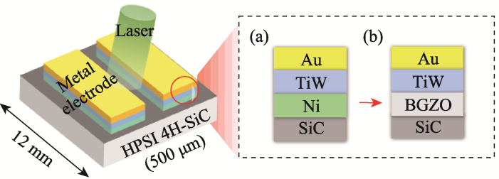
图1 SiC PCSS电极结构图
Fig. 1 Diagrams of SiC PCSS electrode components (a) Au/TiW/Ni/SiC; (b) Au/TiW/BGZO/SiC
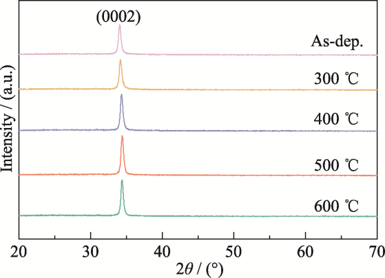
图2 退火前和不同退火温度下BGZO薄膜的XRD图谱
Fig. 2 XRD patterns of BGZO thin films before and after annealing at different temperatures
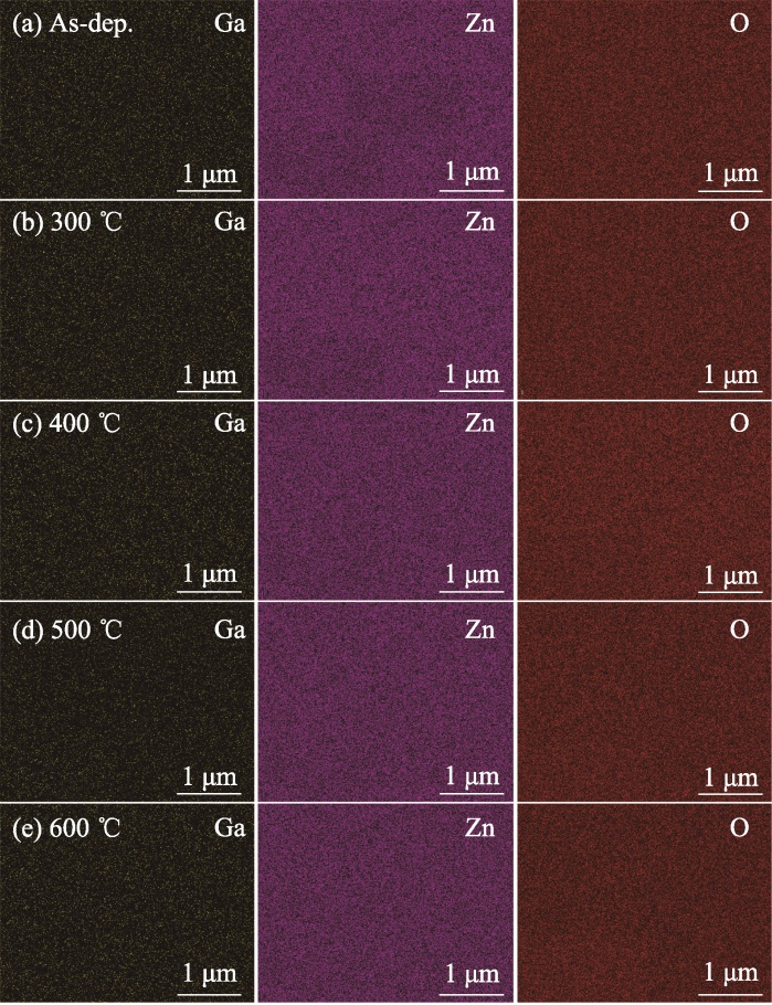
图3 退火前和不同退火温度下BGZO薄膜的EDS测试结果
Fig. 3 EDS test results of BGZO thin films before and after annealing at different temperatures (a) As-dep.; (b) 300 ℃; (c) 400 ℃; (d) 500 ℃; (e) 600 ℃
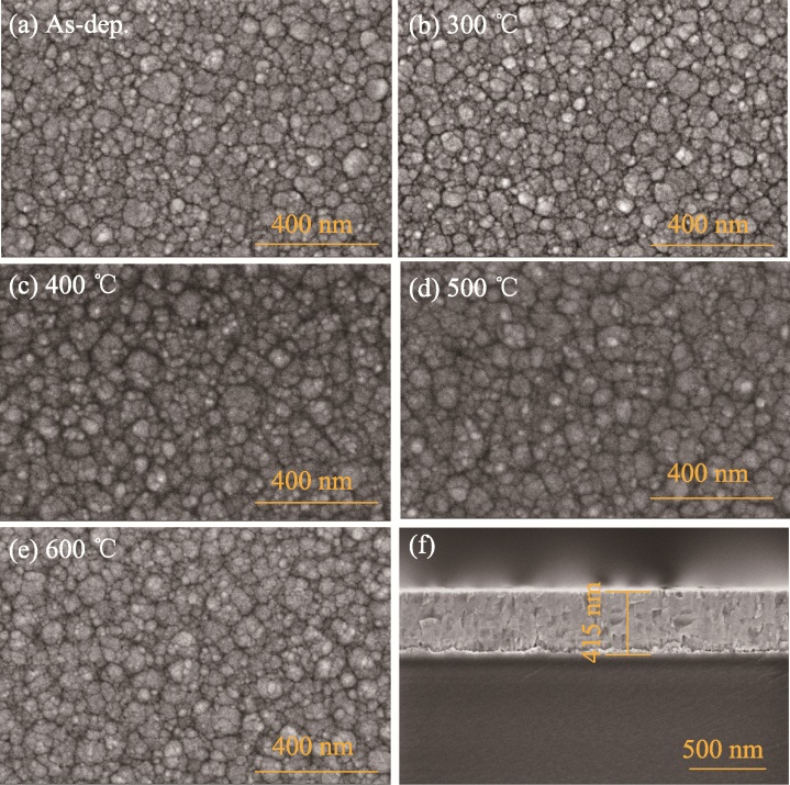
图4 退火前和不同退火温度下BGZO薄膜的SEM照片
Fig. 4 SEM images of BGZO thin films before and after annealing at different temperatures (a) As-dep.; (b) 300 ℃; (c) 400 ℃; (d) 500 ℃; (e) 600 ℃
| Temperature/℃ | Zn/Ga |
|---|---|
| As-dep. | 43.65 |
| 300 | 43.38 |
| 400 | 33.90 |
| 500 | 34.54 |
| 600 | 32.82 |
表1 退火前和不同退火温度下BGZO薄膜Zn/Ga比
Table 1 Zn/Ga ratio of BGZO thin films before and after annealing at different temperatures
| Temperature/℃ | Zn/Ga |
|---|---|
| As-dep. | 43.65 |
| 300 | 43.38 |
| 400 | 33.90 |
| 500 | 34.54 |
| 600 | 32.82 |
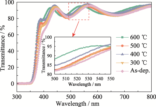
图5 退火前和不同退火温度下BGZO薄膜的光学透过率
Fig. 5 Transmittance of BGZO thin films before and after annealing at different temperatures
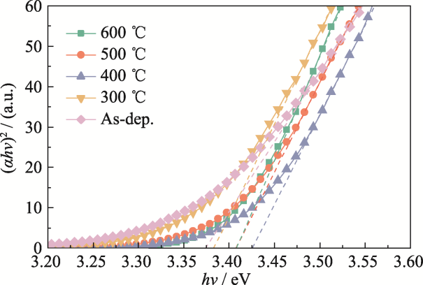
图6 退火前和不同退火温度下BGZO薄膜的Tauc图
Fig. 6 Tauc plots of BGZO thin films before and after annealing at different temperatures
| Temperature/℃ | Bandgap/eV |
|---|---|
| As-dep. | 3.37 |
| 300 | 3.38 |
| 400 | 3.43 |
| 500 | 3.41 |
| 600 | 3.41 |
表2 退火前和不同退火温度下BGZO薄膜的光学禁带宽度
Table 2 Optical bandgap of BGZO thin films before and after annealing at different temperatures
| Temperature/℃ | Bandgap/eV |
|---|---|
| As-dep. | 3.37 |
| 300 | 3.38 |
| 400 | 3.43 |
| 500 | 3.41 |
| 600 | 3.41 |
| Temperature/℃ | Carrier concentration/ (×1020, cm-3) | Hall mobility/ (cm2·V-1·s-1) | Resistivity/ (Ω·cm) |
|---|---|---|---|
| 300 | 0.278 | 0.62 | 0.362 |
| 400 | 1.382 | 1.78 | 0.028 |
| 500 | 1.834 | 2.64 | 0.014 |
| 600 | 0.783 | 5.06 | 0.016 |
表3 不同退火温度下BGZO薄膜的电学性能
Table 3 Electrical properties of BGZO thin films at different annealing temperatures
| Temperature/℃ | Carrier concentration/ (×1020, cm-3) | Hall mobility/ (cm2·V-1·s-1) | Resistivity/ (Ω·cm) |
|---|---|---|---|
| 300 | 0.278 | 0.62 | 0.362 |
| 400 | 1.382 | 1.78 | 0.028 |
| 500 | 1.834 | 2.64 | 0.014 |
| 600 | 0.783 | 5.06 | 0.016 |
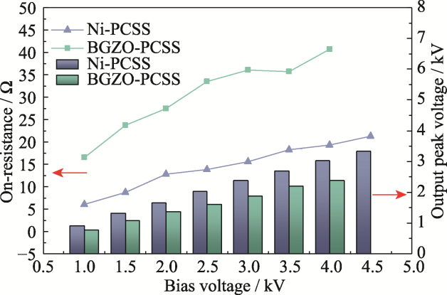
图7 PCSS导通特性
Fig. 7 Output characteristics of PCSS
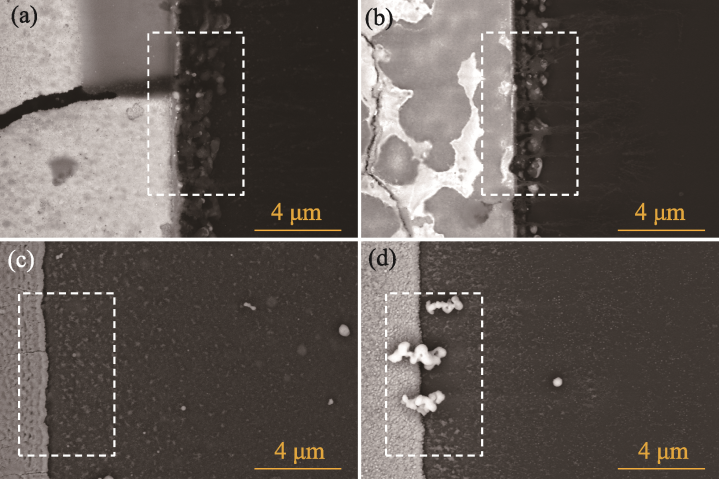
图8 PCSS电极边缘的SEM照片
Fig. 8 SEM images of PCSS electrode edge (a) Ni-PCSS-1; (b) Ni-PCSS-2; (c) BGZO-PCSS-1; (d) BGZO-PCSS-2
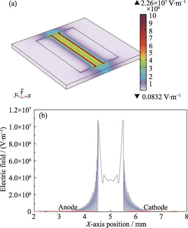
图9 PCSS电极边缘电场仿真
Fig. 9 Electric field simulation of electrode edge (a) Electrode edge electric field simulation; (b) Distribution of electric field strength at the edge of simulated electrode
| [1] |
ZHANG D H, XU Z, CHENG G, et al. Strongly enhanced THz generation enabled by a graphene hot-carrier fast lane. Nature Communications, 2022, 13: 6404.
DOI PMID |
| [2] |
HE T, YI M Y, NIU X Y, et al. The trade-off between microwave frequency and output power in sic photoconductive switches based on carrier lifetime. IEEE Transactions on Electron Devices, 2025, 72(1): 169.
DOI URL |
| [3] |
SUN Q, WANG Y T, GUO H, et al. Performance of a side-gap- triggered vanadium-compensated 4H-SiC photoconductive switch. IEEE Transactions on Electron Devices, 2025, 72(6): 3114.
DOI URL |
| [4] |
CHU X, LIU J, XUN T, et al. MHz repetition frequency, hundreds kilowatt, and sub-nanosecond agile pulse generation based on linear 4H-SiC photoconductive semiconductor. IEEE Transactions on Electron Devices, 2022, 69(2): 597.
DOI URL |
| [5] |
MAJDA-ZDANCEWICZ E, SUPRONIUK M, PAWLOWSKI M, et al. Current state of photoconductive semiconductor switch engineering. Opto-Electronics Review, 2018, 26(2): 92.
DOI URL |
| [6] |
FENG Z, LUAN C, XIAO L, et al. Performance of a novel rear-triggered 4H-SiC photoconductive semiconductor switch. IEEE Transactions on Electron Devices, 2023, 70(2): 627.
DOI URL |
| [7] |
MEYERS V, VOSS L, FLICKER J D, et al. Photoconductive semiconductor switches: materials, physics, and applications. Applied Sciences, 2025, 15(2): 645.
DOI URL |
| [8] |
MAUCH D, SULLIVAN W, BULLICK A, et al. High power lateral silicon carbide photoconductive semiconductor switches and investigation of degradation mechanisms. IEEE Transactions on Plasma Science, 2015, 43(6): 2021.
DOI URL |
| [9] |
WANG L, JIA Y, LIU J. Photoconductive semiconductor switch-based triggering with 1 ns jitter for trigatron. Matter and Radiation at Extremes, 2018, 3(5): 256.
DOI URL |
| [10] |
SULLIVAN J S, STANLEY J R. Wide bandgap extrinsic photoconductive switches. IEEE Transactions on Plasma Science, 2008, 36(5): 2528.
DOI URL |
| [11] |
WANG L, CHU X, WU Q, et al. Effects of high-field velocity saturation on the performance of V-doped 6H silicon-carbide photoconductive switches. IEEE Journal of Emerging and Selected Topics in Power Electronics, 2021, 9(4): 4879.
DOI URL |
| [12] |
CHEN S T, XU M, LV R D, et al. Photon absorption effects on the transient carrier dynamics in high-purity 4H-SiC PCSS. IEEE Electron Device Letters, 2025, 46(2): 278.
DOI URL |
| [13] |
YANG F, WANG Z, LIANG Z, et al. Electrical performance advancement in SiC power module package design with kelvin drain connection and low parasitic inductance. IEEE Journal of Emerging and Selected Topics in Power Electronics, 2019, 7(1): 84.
DOI URL |
| [14] |
WEITZEL C E, PALMOUR J W, CARTER C H, et al. Silicon carbide high-power devices. IEEE Transactions on Electron Devices, 1996, 43(10): 1732.
DOI URL |
| [15] |
HUANG J, HU L, YANG X H, et al. Modeling and simulation of Fe-doped GaN PCSS in high-power microwave. IEEE Transactions on Electron Devices, 2023, 70(7): 3489.
DOI URL |
| [16] |
ZHENG Z, JIANG S N, SUN Q, et al. Effects of illumination on space-charge-limited current in 4H-SiC photoconductive semiconductor switches. IEEE Transactions on Electron Devices, 2025, 72(8): 4290.
DOI URL |
| [17] |
XU B J, HAN X F, XU S C, et al. Optimization of the thermal field of 8-inch SiC crystal growth by PVT method with " 3 separation heater method". Journal of Crystal Growth, 2023, 614: 127238.
DOI URL |
| [18] |
FENG Z Y, XIAO L F, LUAN C B, et al. Dependence of conduction characteristics on compensation type and lattice structure of SiC photoconductive semiconductor switches. Applied Optics, 2021, 60(11): 3182.
DOI URL |
| [19] |
CICHON S, MACHÁC P, BARDA B, et al. Raman study of Ni and Ni silicide contacts on 4H-and 6H-SiC. Thin Solid Films, 2012, 520(13): 4378.
DOI URL |
| [20] |
ROGOWSKI J, KUBIAK A. Investigation of microstructure and chemical composition of Ni contacts to n-type 4H-SiC. Materials Science and Engineering: B, 2012, 177(15): 1318.
DOI URL |
| [21] | ERVIN M H, JONES K A, LEE U, et al. Approach to optimizing n-SiC Ohmic contacts by replacing the original contacts with a second metal. Journal of Vacuum Science & Technology B, 2006, 24(3): 1185. |
| [22] |
XIAO L F, YANG X L, DUAN P, et al. Effect of electron avalanche breakdown on a high-purity semi-insulating 4H-SiC photoconductive semiconductor switch under intrinsic absorption. Applied Optics, 2018, 57(11): 2804.
DOI URL |
| [23] |
ZHU K, JOHNSTONE D, LEACH J, et al. High power photoconductive switches of 4H SiC with Si3N4 passivation and n+-GaN subcontact. Superlattices and Microstructures, 2007, 41(4): 264.
DOI URL |
| [24] |
ZHENG Z, HUANG W, HAN W W, et al. Analyzing the effects of aluminum-doped ZnO and Ag layers for the transparent electrode vertical PCSS. IEEE Transactions on Electron Devices, 2020, 67(6): 2414.
DOI URL |
| [25] |
CAO P H, HUANG W, GUO H, et al. Performance of a vertical 4H-SiC photoconductive switch with AZO transparent conductive window and silver mirror reflector. IEEE Transactions on Electron Devices, 2018, 65(5): 2047.
DOI URL |
| [26] |
HUANG J, HU L, MA Z Z, et al. Study on photoelectric efficiency and failure mechanism of high purity 4H-SiC PCSS. IEEE Transactions on Electron Devices, 2023, 70(11): 5762.
DOI URL |
| [27] |
CHEN Z P, HUANG Z C, SUN Q, et al. Analysis of the influence of defect evolution on the performance and damage of 4H-SiC photoconductive semiconductor switches. Journal of Applied Physics, 2025, 137(17): 175706.
DOI URL |
| [28] |
ZENG L L, WANG L N, NIU X Y, et al. Characteristics comparison of SiC and GaN extrinsic vertical photoconductive switches. IEEE Journal of the Electron Devices Society, 2024, 12: 249.
DOI URL |
| [29] |
HUANG W, CHANG S H, LIU X C, et al. Effects of substrate crystallinity on the on-state resistance of 6H-SiC photoconductive switches. Journal of Materials Research, 2013, 28(1): 38.
DOI URL |
| [30] |
HAO W, LIU X C, ZHENG Z, et al. Performance of lateral 4H-SiC photoconductive semiconductor switches by extrinsic backside trigger. Journal of Inorganic Materials, 2024, 39(9): 1070.
DOI URL |
| [1] | 刘雷敏, 罗红心, 何玉梅, 金利民, 李永杰, 刘静雯, 魏玉全, 孙安乐, 陈忠明, 刘学建, 殷杰, 黄政仁. 先进光源装置用碳化硅反射镜性能研究[J]. 无机材料学报, 2026, 41(6): 805-813. |
| [2] | 曹娟, 吴西士, 刘泽华, 裴兵兵, 韩建燊, 刘欢, 杨亦天, 吴海波, 黄政仁. 晶粒尺寸对常压固相烧结SiC陶瓷断裂强度Weibull分布的影响[J]. 无机材料学报, 2026, 41(2): 217-224. |
| [3] | 王鲁杰, 张玉新, 李彤阳, 于源, 任鹏伟, 王建章, 汤华国, 姚秀敏, 黄毅华, 刘学建, 乔竹辉. 深海服役环境下碳化硅陶瓷材料的腐蚀及磨损行为[J]. 无机材料学报, 2025, 40(7): 799-807. |
| [4] | 李紫薇, 弓伟露, 崔海峰, 叶丽, 韩伟健, 赵彤. 前驱体法制备(Zr, Hf, Nb, Ta, W)C-SiC复相陶瓷及性能研究[J]. 无机材料学报, 2025, 40(3): 271-280. |
| [5] | 王浩, 刘学超, 郑重, 潘秀红, 徐锦涛, 朱新锋, 陈锟, 邓伟杰, 汤美波, 郭辉, 高攀. 非本征背照触发平面型4H-SiC光导开关性能研究[J]. 无机材料学报, 2024, 39(9): 1070-1076. |
| [6] | 王康龙, 殷杰, 陈晓, 王力, 刘学建, 黄政仁. 颗粒级配对选区激光烧结打印结合常压固相烧结制备碳化硅陶瓷性能的影响[J]. 无机材料学报, 2024, 39(7): 754-760. |
| [7] | 孙川, 何鹏飞, 胡振峰, 王荣, 邢悦, 张志彬, 李竞龙, 万春磊, 梁秀兵. 含有石墨烯阵列的SiC基陶瓷材料的制备与力学性能[J]. 无机材料学报, 2024, 39(3): 267-273. |
| [8] | 徐昊, 钱伟, 花银群, 叶云霞, 戴峰泽, 蔡杰. 皮秒激光加工的微织构对碳化硅润湿性的影响[J]. 无机材料学报, 2023, 38(8): 923-930. |
| [9] | 陈强, 白书欣, 叶益聪. 热管理用高导热碳化硅陶瓷基复合材料研究进展[J]. 无机材料学报, 2023, 38(6): 634-646. |
| [10] | 顾薛苏, 殷杰, 王康龙, 崔崇, 梅辉, 陈忠明, 刘学建, 黄政仁. 颗粒级配对黏结剂喷射打印碳化硅陶瓷性能的影响[J]. 无机材料学报, 2023, 38(12): 1373-1378. |
| [11] | 吴松泽, 周洋, 李润丰, 刘晓倩, 李翠伟, 黄振莺. 铁尾矿及其反应烧结多孔陶瓷的制备与性能研究[J]. 无机材料学报, 2023, 38(10): 1193-1199. |
| [12] | 欧阳琴, 王艳菲, 徐剑, 李寅生, 裴学良, 莫高明, 李勉, 李朋, 周小兵, 葛芳芳, 张崇宏, 何流, 杨磊, 黄政仁, 柴之芳, 詹文龙, 黄庆. 核用碳化硅纤维增强碳化硅复合材料研究进展[J]. 无机材料学报, 2022, 37(8): 821-840. |
| [13] | 阮景, 杨金山, 闫静怡, 游潇, 王萌萌, 胡建宝, 张翔宇, 丁玉生, 董绍明. 三维碳化硅纳米线增强碳化硅陶瓷基复合材料的电磁屏蔽性能[J]. 无机材料学报, 2022, 37(5): 579-584. |
| [14] | 阮景, 杨金山, 闫静怡, 游潇, 王萌萌, 胡建宝, 张翔宇, 丁玉生, 董绍明. 碳化硅纳米线增强多孔碳化硅陶瓷基复合材料的制备[J]. 无机材料学报, 2022, 37(4): 459-466. |
| [15] | 李陇彬, 薛玉冬, 胡建宝, 杨金山, 张翔宇, 董绍明. 碳化硅纳米线增韧碳化硅纤维/碳化硅基体损伤行为研究[J]. 无机材料学报, 2021, 36(10): 1111-1117. |
| 阅读次数 | ||||||
|
全文 |
|
|||||
|
摘要 |
|
|||||