无机材料学报 ›› 2021, Vol. 36 ›› Issue (6): 570-578.DOI: 10.15541/jim20200361 CSTR: 32189.14.10.15541/jim20200361
所属专题: 能源材料论文精选(2021); 【虚拟专辑】太阳能电池(2020~2021)
武晓玮1,2( ), 李佳艳1,2()
收稿日期:2020-06-30
修回日期:2020-08-30
出版日期:2021-06-20
网络出版日期:2020-10-10
通讯作者:
李佳艳, 副教授. E-mail: lijiayan@dlut.edu.cn
作者简介:武晓玮(1991-), 男, 博士研究生. E-mail: wuxiaowei261@163.com
基金资助:
WU Xiaowei1,2(), LI Jiayan1,2()
Received:2020-06-30
Revised:2020-08-30
Published:2021-06-20
Online:2020-10-10
Contact:
LI Jiayan, associate professor. E-mail: lijiayan@dlut.edu.cn
About author:WU Xiaowei(1991-), male, PhD candidate. E-mail: wuxiaowei261@163.com
Supported by:摘要:
在多晶硅太阳能电池的生产过程中, 金刚线切割技术(Diamond wire sawn, DWS)具有切割速度快、精度高、原材料损耗少等优点, 受到了广泛关注。金刚线切割多晶硅表面形成的损伤层较浅, 与传统的酸腐蚀制绒技术无法匹配, 金属催化化学腐蚀法应运而生。金属催化化学腐蚀法制绒具有操作简单、结构可控且易形成高深宽比的绒面等优点, 具有广阔的应用前景。本文总结了不同类型的金属催化剂在制绒过程中的腐蚀机理及其形成的绒面结构, 深入分析和讨论了具有代表性的银、铜的单一及复合催化腐蚀过程及绒面结构和电池片性能。最后对金刚线切割多晶硅片表面的金属催化化学腐蚀法存在的问题进行了分析, 并展望了未来的研究方向。
中图分类号:
武晓玮, 李佳艳. 多晶硅表面金属催化化学腐蚀法制绒研究现状[J]. 无机材料学报, 2021, 36(6): 570-578.
WU Xiaowei, LI Jiayan. Texturing Technology on Multicrystalline Silicon Wafer by Metal-catalyzed Chemical Etching: a Review[J]. Journal of Inorganic Materials, 2021, 36(6): 570-578.
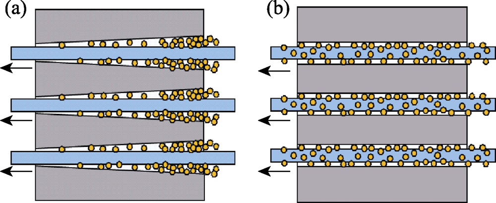
图1 (a)砂浆切割和(b)金刚线切割示意图
Fig. 1 Schematic diagram of (a) MWSS cut technique and (b) DWS cut technique

图2 (a, b)砂浆切割和(c, d)金刚线切割后多晶硅片表面形貌SEM照片
Fig. 2 SEM images of (a, b) MWSS cut and (c, d) DWS cut multicrystalline silicon wafer surface
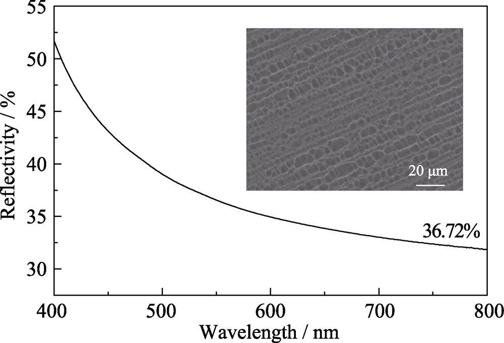
图3 酸腐蚀法制绒后硅片表面SEM形貌和反射率曲线
Fig. 3 Surface SEM morphology and reflectivity for texture surface of silicon wafer by acid etching

图4 MCCE法原理示意图[18]
Fig. 4 Schematic diagram of MCCE[18]

图5 (a)纳米绒面、(b)微米绒面及(c)纳米-微米复合绒面SEM表面形貌照片[31]
Fig. 5 SEM images of silicon surfaces with (a) nano-texture, (b) micro-texture and (c) nano-micro-texture[31]
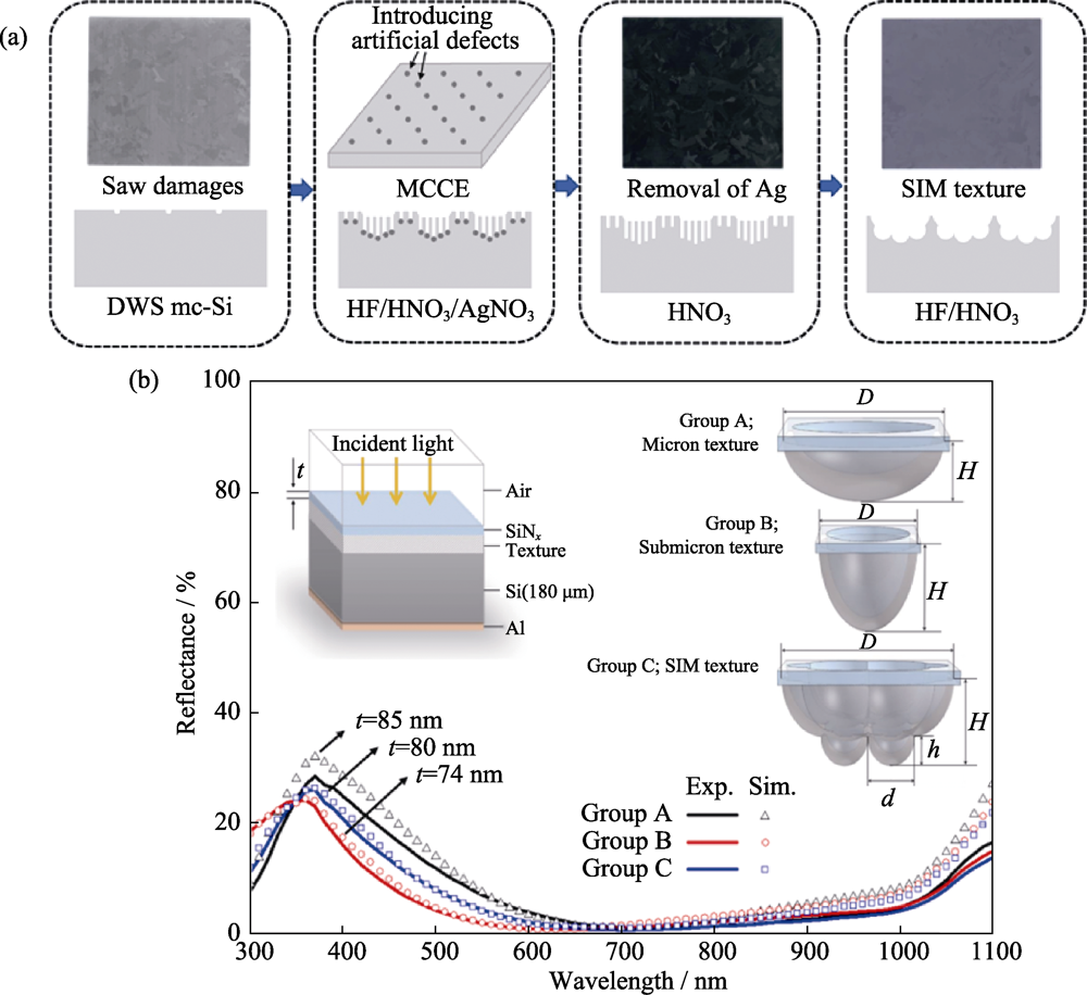
图6 (a)DWS多晶硅片表面制备亚微米级(SIM)绒面的过程示意图和(b)三种绒面结构的反射率结果[33]
Fig. 6 (a) Schematic illustration of the main steps to prepare the submicron-in-micron (SIM) texture on the DWS mc-Si wafer and (b) experimental reflectance (curves) and simulated reflectance (scatter points) of three samples[33]
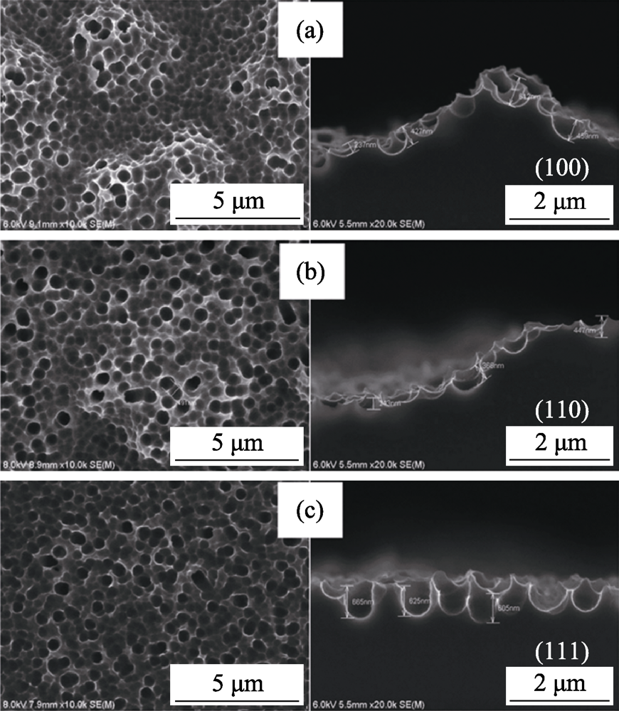
图7 碱、Ag-MCCE和后腐蚀处理获得的不同晶面的硅片表面和截面SEM照片[34]
Fig. 7 Surface and cross-sectional SEM images of mc-Si grains after etching by alkali, Ag-MCCE and post-etching with different orientations[34] (a) (100); (b) (110); (c) (111)
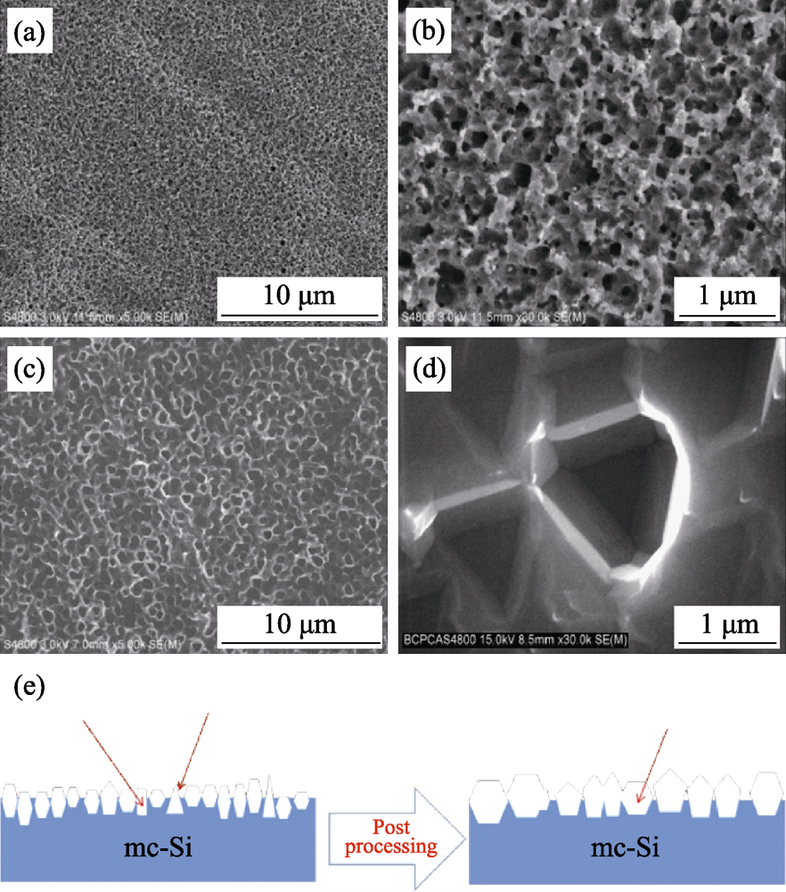
图8 Cu-MCCE制绒后采用后处理工艺(a, b)前和(c, d)后的硅片形貌图以及(e)后处理工艺示意图[41]
Fig. 8 SEM images of Si nanostructures produced by Cu-MCCE method (a,b) before and (c,d) after the post-processing treatment and (e) schematic diagram of post-processing treatment[41]

图9 (a)Ag-MCCE和(b)Cu-MCCE处理后的硅片截面形貌SEM照片, 以及(c)单独的Cu-MCCE、Ag-MCCE和Ag-Cu复合制绒过程的原理图[45]
Fig. 9 Cross-sectional SEM images of Si wafers after (a) Ag-MCCE and (b) Cu-MCCE, and (c) schematics of etching process by single Cu- and Ag-catalyzed chemical etching and Ag/Cu-cocatalyzed chemical etching[45]
| Catalyst | Method | Ra | ηb | Ref. |
|---|---|---|---|---|
| Ag | Ag-MCCE + HF/HNO3+NaOH | 15.9% | 18.45% | [ |
| Ag | Artificial defects (HF/HNO3/AgNO3)+HF/HNO3 | 19% | 19.07% | [ |
| Ag | Alkali etching+Ag-MCCE+post etching | 16.85% | 19.4% | [ |
| Ag | Ag deposition (additive)+etching | 16.04% | 19.51% | [ |
| Ag | Ag deposition+etching (additive) | 18.17% | 19.56% | [ |
| Ag | HF/HNO3+Ag-MCCE+RIE | - | 20.69% | [ |
| Ag | Ag-MCCE | 23.7% | 20.89% | [ |
| Ag | Ag-MCCE+Modification by acid etching | 19.46% | 19.07% | [ |
| Ag | HF/HNO3+Ag-MCCE+NSR process | 8.26% | 17.96% | [ |
| Ag | HF/HNO3+Ag-MCCE+HF/HNO3 | 18.4% | 18.7% | [ |
| Cu | Cu-MCCE+post etching (HF/HNO3/H3PO4) | - | 18.88% | [ |
| Cu | Cu-MCCE+HF/HNO3 | 18.21% | 19.06% | [ |
| Cu | Cu-MCCE | 22.4% | 19.03% | [ |
| Ag-Cu | Cu/Ag-MCCE | 12.08% | 19.49% | [ |
| Ag-Cu | Alkali pretreatment (additive)+Cu/Ag-MCCE+post etching | 15.52% | 18.91% | [ |
| Ag-Cu | Cu/Ag-MCCE + NSR (H2O2/NaF) | 16.50% | 18.71% | [ |
| Ag-Cu | Cu/Ag-MCCE + NSR (H2O2/NaF) | 16.85% | 19.10% | [ |
| Ni | Ni-MCCE | - | 16.60% | [ |
| Cu-Ni | Cu/Ni-MCCE (Cu(NO3)2+NiSO4+HF+H2O2) | 18.53% | - | [ |
表1 金刚线切割多晶硅片表面不同MCCE方法制绒后的性能对比
Table 1 Performances for texture surfaces of DWS cut multicrystalline silicon prepared via different MCCE methods
| Catalyst | Method | Ra | ηb | Ref. |
|---|---|---|---|---|
| Ag | Ag-MCCE + HF/HNO3+NaOH | 15.9% | 18.45% | [ |
| Ag | Artificial defects (HF/HNO3/AgNO3)+HF/HNO3 | 19% | 19.07% | [ |
| Ag | Alkali etching+Ag-MCCE+post etching | 16.85% | 19.4% | [ |
| Ag | Ag deposition (additive)+etching | 16.04% | 19.51% | [ |
| Ag | Ag deposition+etching (additive) | 18.17% | 19.56% | [ |
| Ag | HF/HNO3+Ag-MCCE+RIE | - | 20.69% | [ |
| Ag | Ag-MCCE | 23.7% | 20.89% | [ |
| Ag | Ag-MCCE+Modification by acid etching | 19.46% | 19.07% | [ |
| Ag | HF/HNO3+Ag-MCCE+NSR process | 8.26% | 17.96% | [ |
| Ag | HF/HNO3+Ag-MCCE+HF/HNO3 | 18.4% | 18.7% | [ |
| Cu | Cu-MCCE+post etching (HF/HNO3/H3PO4) | - | 18.88% | [ |
| Cu | Cu-MCCE+HF/HNO3 | 18.21% | 19.06% | [ |
| Cu | Cu-MCCE | 22.4% | 19.03% | [ |
| Ag-Cu | Cu/Ag-MCCE | 12.08% | 19.49% | [ |
| Ag-Cu | Alkali pretreatment (additive)+Cu/Ag-MCCE+post etching | 15.52% | 18.91% | [ |
| Ag-Cu | Cu/Ag-MCCE + NSR (H2O2/NaF) | 16.50% | 18.71% | [ |
| Ag-Cu | Cu/Ag-MCCE + NSR (H2O2/NaF) | 16.85% | 19.10% | [ |
| Ni | Ni-MCCE | - | 16.60% | [ |
| Cu-Ni | Cu/Ni-MCCE (Cu(NO3)2+NiSO4+HF+H2O2) | 18.53% | - | [ |
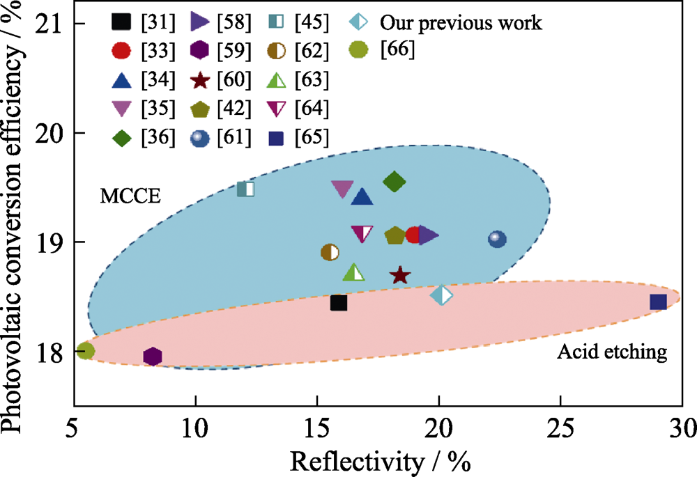
图10 电池片光电转换效率与绒面反射率之间的关系图[31,33-36,42,45,58-65]
Fig. 10 Relation between η of solar cells and reflectivity of texture surface[31,33-36,42,45,58-65]
| Method | Advantages | Disadvantages | η |
|---|---|---|---|
| Ag-MCCE | Mature technology, easy to form nanostructure, stable performance | High cost, difficult to recycle waste liquid | 20.89% |
| Cu-MCCE | Low cost, easy to remove residual Cu, significantly reduce the impact of saw marks | Easy to form the dense film, decreased etching rate, essential oxidants | 19.06% |
| MCCE-additive | Uniform size, stable performance | Organic compounds increasing the cost of waste liquid treatment | 19.56% |
| Composite MCCE | Composite structure | Complicated process, and difficult to recycle the waste liquid | 19.49% |
| Other metal-MCCE | Low cost, composite structure | Inmature | 16.60% |
表2 金刚线切割多晶硅片表面不同MCCE方法的对比
Table 2 Comparison of making texture surface on DWS cut multicrystalline silicon by different MCCE methods
| Method | Advantages | Disadvantages | η |
|---|---|---|---|
| Ag-MCCE | Mature technology, easy to form nanostructure, stable performance | High cost, difficult to recycle waste liquid | 20.89% |
| Cu-MCCE | Low cost, easy to remove residual Cu, significantly reduce the impact of saw marks | Easy to form the dense film, decreased etching rate, essential oxidants | 19.06% |
| MCCE-additive | Uniform size, stable performance | Organic compounds increasing the cost of waste liquid treatment | 19.56% |
| Composite MCCE | Composite structure | Complicated process, and difficult to recycle the waste liquid | 19.49% |
| Other metal-MCCE | Low cost, composite structure | Inmature | 16.60% |
| [1] |
ADEBISI J A, AGUNSOYE J O, BELLO S A, et al. Potential of producing solar grade silicon nanoparticles from selected agro-wastes: a review. Sol. Energy, 2017,142:68-86.
DOI URL |
| [2] |
YIN Y, GAO Y, LI X, et al. Experimental study on slicing photovoltaic polycrystalline silicon with diamond wire saw. Mat. Sci. Semicon. Proc., 2020,106:104779.
DOI URL |
| [3] |
BASHER M K, MISHAN R, BISWAS S, et al. Study and analysis the Cu nanoparticle assisted texturization forming low reflective silicon surface for solar cell application. AIP Adv., 2019,9:075118.
DOI URL |
| [4] | ANDREANI L C, BOZZOLA A, KOWALCZEWSKI P, et al. Silicon solar cells: toward the efficiency limits. Adv. Phys. X, 2019,4(1):1548305. |
| [5] |
HUANG B J, ZHAO J, CHAI J Y, et al. Environmental influence assessment of China's multi-crystalline silicon (multi-Si) photovoltaic modules considering recycling process. Sol. Energy, 2017,143:132-141.
DOI URL |
| [6] |
MÖLLER H J, FUNKE C, RINIO M, et al. Multicrystalline silicon for solar cells. Thin Solid Films, 2005,487(1):179-187.
DOI URL |
| [7] |
MEINEL B, KOSCHWITZ T, BLOCKS C, et al. Comparison of diamond wire cut and silicon carbide slurry processed silicon wafer surfaces after acidic texturisation. Mat. Sci. Semicon. Proc., 2014,26:93-100.
DOI URL |
| [8] |
WU Y F, CHEN Y M. Separation of silicon and silicon carbide using an electrical field. Sep. Purif. Technol., 2009,68(1):70-74.
DOI URL |
| [9] |
HARDIN C W, QU J, SHIH A J. Fixed abrasive diamond wire saw slicing of single-crystal silicon carbide wafers. Mater. Manuf. Processes, 2004,19(2):355-367.
DOI URL |
| [10] | QIU M B, HUANG Y H, LIU Z D, et al. A review of the fabrication methods for solar silicon wafer. Mechanical Science and Technology for Aerospace Engineering, 2008,27(8):1017-1020. |
| [11] | CAI E, TANG B, FAHRNER W R, et al. Characterization of the Surfaces Generated by Diamond Cutting of Crystalline Silicon. 26th European Photovoltaic Solar Energy Conference and Exhibition. Hamburg, 2011: 1884-1886. |
| [12] | CHEN C C A, CHAO P H. Surface texture analysis of fixed and free abrasive machining of silicon substrates for solar cell. Adv. Mater. Res., 2010, 126-128:177-180. |
| [13] | BIDIVILLE A, WASMER K, KRAFT R, et al. Diamond Wire-sawn Silicon Wafers-from the Lab to the Cell Production. 24th European Photovoltaic Solar Energy Conference and Exhibition. Hamburg, 2009: 1400-1405. |
| [14] |
LIPPOLD M, BUCHHOLZ F, GONDEK C, et al. Texturing of SiC-slurry and diamond wire sawn silicon wafers by HF-HNO3-H2SO4 mixtures. Sol. Energ. Mat. Sol. C, 2014,127:104-110.
DOI URL |
| [15] |
MEMMING R, SCHWANDT G. Anodic dissolution of silicon in hydrofluoric acid solutions. Surf. Sci., 1966,4(2):109-124
DOI URL |
| [16] |
XIAO Z G, GENG G Y, WEI X Q, et al. On the mechanism of the vapor etching of diamond wire sawn multi-crystalline silicon wafers for texturing. Mat. Sci. Semicon. Proc., 2016,53:8-12.
DOI URL |
| [17] |
JANSEN H, DEBOER M, LEGTENBERG R, et al. The black silicon method-a universal method for determining the parameter setting of a fluorine-based reactive ion etcher in deep silicon trench etching with profile control. J. Micromech. Microeng., 1995,5(2):115-120.
DOI URL |
| [18] |
HUANG Z P, GEYER N, WERNER P, et al. Metal-assisted chemical etching of silicon: a review. Adv. Mater., 2011,23(2):285-308.
DOI URL |
| [19] |
HSU C, WU J R, LU Y T, et al. Fabrication and characteristics of black silicon for solar cell applications: an overview. Mat. Sci. Semicon. Proc., 2014,25:2-17.
DOI URL |
| [20] |
DIMOVA-MALINOVSKA D, SENDOVA-VASSILEVA M, TZENOV N, et al. Preparation of thin porous silicon layers by stain etching. Thin Solid Films, 1997,297(1/2):9-12.
DOI URL |
| [21] |
LI X, BOHN P W. Metal-assisted chemical etching in HF/H2O2 produces porous silicon. Appl. Phys. Lett., 2000,77(16):2572-2574.
DOI URL |
| [22] |
HUANG Z P, WU Y, FANG H, et al. Large-scale Si1-xGex quantum dot arrays fabricated by templated catalytic etching. Nanotechnology, 2006,17(5):1476-1480.
DOI URL |
| [23] |
HUANG Z, SHIMIZU T, SENZ S, et al. Ordered arrays of vertically aligned [110] silicon nanowires by suppressing the crystallographically preferred <100> etching directions. Nano Lett., 2009,9(7):2519-2525.
DOI URL |
| [24] |
PENG K Q, HU J J, YAN Y J, et al. Fabrication of single-crystalline silicon nanowires by scratching a silicon surface with catalytic metal particles. Adv. Funct. Mater., 2006,16(3):387-394.
DOI URL |
| [25] |
CHATTOPADHYAY S, BOHN P W. Direct-write patterning of microstructured porous silicon arrays by focused-ion-beam Pt deposition and metal-assisted electroless etching. J. Appl. Phys., 2004,96(11):6888-6894.
DOI URL |
| [26] |
NIU Y C, LIU H T, LIU X J, et al. Study on nano-pores enlargement during Ag-assisted electroless etching of diamond wire sawn polycrystalline silicon wafers. Mat. Sci. Semicon. Proc., 2016,56:119-126.
DOI URL |
| [27] |
SU G Y, DAI X W, SUN H C, et al. The study of the defect removal etching of black silicon for diamond wire sawn multi-crystalline silicon solar cells. Sol. Energy, 2018,170:95-101.
DOI URL |
| [28] |
CAO F, CHEN K X, ZHANG J J, et al. Next-generation multi-crystalline silicon solar cells: diamond-wire sawing, nano-texture and high efficiency. Sol. Energ. Mat. Sol. C, 2015,141:132-138.
DOI URL |
| [29] |
KUMAGAI A. Texturization using metal catalyst wet chemical etching for multicrystalline diamond wire sawn wafer. Sol. Energ. Mat. Sol. C, 2015,133:216-222.
DOI URL |
| [30] | PENG K, FANG H, HU J, et al. Metal-particle-induced, highly localized site-specific etching of Si and formation of single-crystalline Si nanowires in aqueous fluoride solution. Chemistry, 2006,12(30):7942-7947. |
| [31] |
ZHUANG Y F, ZHONG S H, HUANG Z G, et al. Versatile strategies for improving the performance of diamond wire sawn mc-Si solar cells. Sol. Energ. Mat. Sol. C, 2016,153:18-24.
DOI URL |
| [32] |
ZHANG P F, JIA R, TAO K, et al. The influence of Ag-ion concentration on the performance of mc-Si silicon solar cells textured by metal assisted chemical etching (MACE) method. Sol. Energ. Mat. Sol. C, 2019,200:109983.
DOI URL |
| [33] |
WU C K, ZOU S, ZHU J Y, et al. Forming submicron in micron texture on the diamond-wire-sawn mc-Si wafer by introducing artificial defects. Prog. Photovoltaics, 2020,28:788-797.
DOI URL |
| [34] |
ZOU S, YE X Y, WU C K, et al. Complementary etching behavior of alkali, metal-catalyzed chemical, and post-etching of multicrystalline silicon wafers. Prog. Photovoltaics, 2019,27(6):511-519.
DOI URL |
| [35] |
LI X P, TAO K, ZHANG D, et al. Development of additive-assisted Ag-MACE for multicrystalline black Si solar cells. Electrochem. Commun., 2020,113:106686.
DOI URL |
| [36] |
LI X P, GAO Z B, ZHANG D, et al. High-efficiency multi-crystalline black silicon solar cells achieved by additive assisted Ag-MACE. Sol. Energy, 2020,195:176-184.
DOI URL |
| [37] |
PENG K Q, ZHU J. Morphological selection of electroless metal deposits on silicon in aqueous fluoride solution. Electrochim Acta, 2004,49(16):2563-2568.
DOI URL |
| [38] |
CAO M, LI S Y, DENG J X, et al. Texturing a pyramid-like structure on a silicon surface via the synergetic effect of copper and Fe(III) in hydrofluoric acid solution. Appl Surf. Sci., 2016,372:36-41.
DOI URL |
| [39] | ZOU Y X, XI F S, QIU J J, et al. Cu-assisted chemical etching of diamond wire sawn multicrystalline silicon wafers for texturing. China Surface Engineering, 2017,30(6):59-66. |
| [40] |
SHENG G Z, ZOU Y X, LI S Y, et al. Controllable nano-texturing of diamond wire sawing polysilicon wafers through low-cost copper catalyzed chemical etching. Mater. Lett., 2018,221:85-88.
DOI URL |
| [41] |
WANG P, XIAO S Q, JIA R, et al. 18.88%-efficient multi-crystalline silicon solar cells by combining Cu-catalyzed chemical etching and post-treatment process. Sol Energy, 2018,169:153-158.
DOI URL |
| [42] |
ZHA J W, WANG T, PAN C F, et al. Constructing submicron textures on mc-Si solar cells via copper-catalyzed chemical etching. Appl. Phys. Lett., 2017,110(9):093901.
DOI URL |
| [43] | ZHENG C F, SHEN H L, PU T, et al. Fabrication and property of anti-reflection structures on multicrystalline silicon by Ag and Cu dually assisted chemical etching. J. Funct. Mater., 2017,48(1):1230-1235. |
| [44] |
WANG S D, CHEN T W. Texturization of diamond-wire-sawn multicrystalline silicon wafer using Cu, Ag, or Ag/Cu as a metal catalyst. Appl. Surf. Sci., 2018,444:530-541.
DOI URL |
| [45] |
CHEN W, LIU Y P, WU J T, et al. High-efficient solar cells textured by Cu/Ag-cocatalyzed chemical etching on diamond wire sawing multicrystalline silicon. ACS Appl. Mater. Inter., 2019,11(10):10052-10058.
DOI URL |
| [46] |
YUE Z H, SHEN H L, JIANG Y, et al. Novel and low reflective silicon surface fabricated by Ni-assisted electroless etching and coated with atomic layer deposited Al2O3 film. Appl. Phys. A-Mater., 2013,114(3):813-817.
DOI URL |
| [47] |
TAKALOO A V, ES F, BAYTEMIR G, et al. Nickel assisted chemical etching for multi-crystalline Si solar cell texturing: a low cost single step alternative to existing methods. Mater. Res. Express, 2018,5(7):075506.
DOI URL |
| [48] |
GAO K, SHEN H L, LIU Y W, et al. Enhanced etching rate of black silicon by Cu/Ni Co-assisted chemical etching process. Mat. Sci. Semicon. Proc., 2018,88:250-255.
DOI URL |
| [49] |
LAI R A, HYMEL T M, NARASIMHAN V K, et al. Schottky barrier catalysis mechanism in metal-assisted chemical etching of silicon. ACS Appl. Mater. Inter., 2016,8(14):8875-8879.
DOI URL |
| [50] |
MAURYA M R, TOUTAM V, SINGH P, et al. Optimization of electroless plating of gold during MACE for through etching of silicon wafer. Mat. Sci. Semicon. Proc., 2019,100:140-144.
DOI URL |
| [51] |
XIE T, SCHMIDT V, PIPPEL E, et al. Gold-enhanced low-temperature oxidation of silicon nanowires. Small, 2008,4(1):64-68.
DOI URL |
| [52] |
BAYTEMIR G, CIFTPINAR E H, TURAN R. Enhanced metal assisted etching method for high aspect ratio microstructures: applications in silicon micropillar array solar cells. Sol. Energy, 2019,194:148-155.
DOI URL |
| [53] |
YAE S, KAWAMOTO Y, TANAKA H, et al. Formation of porous silicon by metal particle enhanced chemical etching in HF solution and its application for efficient solar cells. Electrochem. Commun., 2003,5(8):632-636.
DOI URL |
| [54] |
CHATTOPADHYAY S, LI X, BOHN P W. In-plane control of morphology and tunable photoluminescence in porous silicon produced by metal-assisted electroless chemical etching. J. Appl. Phys., 2002,91(9):6134-6140.
DOI URL |
| [55] |
ZHU B, LIU W J, DING S J, et al. Formation mechanism of heavily doped silicon mesopores induced by Pt nanoparticle-assisted chemical etching. J. Phys. Chem. C, 2018,122(37):21537-21542.
DOI URL |
| [56] |
JIN J, SHEN H, ZHENG P, et al. >20.5% diamond wire sawn multicrystalline silicon solar cells with maskless inverted pyramid like texturing. IEEE J. Photovolt., 2017,7(5):1264-1269.
DOI URL |
| [57] |
SHENG J, WANG W, YE Q H, et al. MACE texture optimization for mass production of high-efficiency multi-crystalline cell and module. IEEE J Photovolt., 2019,9(3):918-925.
DOI URL |
| [58] |
SU G Y, JIA R, DAI X W, et al. The influence of black silicon morphology modification by acid etching to the properties of diamond wire sawn multicrystalline silicon solar cells. IEEE J. Photovolt., 2018,8(4):937-942.
DOI URL |
| [59] |
JIANG Y, SHEN H L, PU T, et al. Hybrid process for texturization of diamond wire sawn multicrystalline silicon solar cell. Phys. Status Solidi-R, 2016,10(12):870-873.
DOI URL |
| [60] |
CHEN K X, ZHA J W, HU F Q, et al. MACE nano-texture process applicable for both single- and multi-crystalline diamond-wire sawn Si solar cells. Sol. Energ. Mat. Sol. C, 2019,191:1-8.
DOI URL |
| [61] |
WU J T, LIU Y P, CHEN Q S, et al. The orientation and optical properties of inverted-pyramid-like structures on multi-crystalline silicon textured by Cu-assisted chemical etching. Sol. Energy, 2018,171:675-680.
DOI URL |
| [62] |
ZHANG P F, SUN H C, TAO K, et al. An 18.9% efficient black silicon solar cell achieved through control of pretreatment of Ag/Cu MACE. J. Mater. Sci. -Mater. El., 2019,30(9):8667-8675.
DOI URL |
| [63] |
ZHENG C F, SHEN H L, PU T, et al. High-efficient solar cells by the Ag/Cu-assisted chemical etching process on diamond-wire-sawn multicrystalline silicon. IEEE J. Photovolt., 2017,7(1):153-156.
DOI URL |
| [64] | SHEN H L, JIANG Y. Investigation on multi-crystalline black silicon and high efficiency solar cell based on inverted pyramid antireflective structure. Journal of Nanjing University of Aeronautics & Astronautics, 2017,49(5):744-752. |
| [65] | SREEJITH K P, SHARMA A K, KUMBHAR S, et al. An additive-free non-metallic energy efficient industrial texturization process for diamond wire sawn multicrystalline silicon wafers. Sol. Energy, 2019,184:162-172. |
| [66] | LIU Y B, ZHANG J N, WANG L, et al. An innovative light trapping structure fabrication method on diamond-wire-sawing multi-crystalline silicon wafers. Chemistry Select, 2018,3(26):7561-7564. |
| [1] | 陈明俊, 缪洪康, 肖英俊, 邓建波, 张翔, 赵九蓬, 李垚. 光-热双响应材料研究进展: 从设计策略到智能窗应用[J]. 无机材料学报, 2026, 41(6): 723-738. |
| [2] | 宋坤洁, 解荣军. 机器学习驱动新型发光材料的研究进展[J]. 无机材料学报, 2026, 41(6): 689-703. |
| [3] | 胡钰晴, 朱一新, 乐先浩, 万青. 钽酸锂晶圆减薄技术及其热释电红外探测器应用进展[J]. 无机材料学报, 2026, 41(6): 764-774. |
| [4] | 刘春帆, 陈科, 葛芳芳, 黄庆. 核用耐铅铋腐蚀涂层的研究进展[J]. 无机材料学报, 2026, 41(6): 775-786. |
| [5] | 胡扬, 谢敏, 张筱怡, 李想, 郭新伟, 姜南, 周文瀚, 张胜利, 曾海波. 计算与数据驱动环保型发光材料的研究进展[J]. 无机材料学报, 2026, 41(6): 704-722. |
| [6] | 王俊卜, 黄泽皑, 杨茗凯, 蒙颖, 周明炜, 周莹. 甲烷转化用抗积碳催化材料研究进展[J]. 无机材料学报, 2026, 41(6): 739-750. |
| [7] | 王金文, 杨振, 周欢, 夏丹, 杨磊. 可注射无机材料及其生物医学应用[J]. 无机材料学报, 2026, 41(6): 751-763. |
| [8] | 李涵涛, 沈强, 罗国强, 王雪飞, 高明, 陈晨. 机械球磨法调控硅基负极材料结构与性能的研究进展[J]. 无机材料学报, 2026, 41(5): 561-572. |
| [9] | 解陈一, 缪花明, 张蔚然, 刘荣军, 王衍飞, 李端. 理论计算在高熵陶瓷领域的研究进展[J]. 无机材料学报, 2026, 41(5): 545-560. |
| [10] | 李璇, 叶奎材, 冯佳音, 邱家军, 钱文昊, 邢敏. 钛基牙种植体表面改性促进软组织封闭的研究进展[J]. 无机材料学报, 2026, 41(4): 432-444. |
| [11] | 彭德招, 李瑞, 王文鸿, 王梓瑞, 章志珍. 钠氯化物固态电解质研究进展[J]. 无机材料学报, 2026, 41(4): 409-420. |
| [12] | 陈坤, 姜勇刚, 冯军宗, 李良军, 胡艺洁, 冯坚. 锆酸镧多孔隔热材料研究进展[J]. 无机材料学报, 2026, 41(4): 421-431. |
| [13] | 韦连金, 齐志杰, 汪信, 朱俊武, 付永胜. 纳米金刚石改性及其在电催化氧还原反应中的应用[J]. 无机材料学报, 2026, 41(3): 273-288. |
| [14] | 刘占一, 李勉, 欧阳晓平, 柴之芳, 黄庆. 干法后处理熔盐中Sr/Cs去除方法的研究进展[J]. 无机材料学报, 2026, 41(2): 150-158. |
| [15] | 孙炼, 张磊磊, 薛泽旭, 吴坤, 陈晔, 李志远, 王鲁凯, 王尊刚. 面向辐射探测应用的零维金属卤化物闪烁体研究进展[J]. 无机材料学报, 2026, 41(2): 159-176. |
| 阅读次数 | ||||||
|
全文 |
|
|||||
|
摘要 |
|
|||||