无机材料学报 ›› 2014, Vol. 29 ›› Issue (6): 614-620.DOI: 10.3724/SP.J.1077.2014.13481 CSTR: 32189.14.SP.J.1077.2014.13481
向卫东1,2, 赵斌宇2, 梁晓娟1, 陈兆平1, 谢翠萍2, 骆 乐2, 张志敏1, 张景峰1,2, 钟家松2
收稿日期:2013-09-24
修回日期:2013-12-06
出版日期:2014-06-20
网络出版日期:2014-05-27
基金资助:XIANG Wei-Dong1,2, ZHAO Bin-Yu2, LIANG Xiao-Juan1, CHEN Zhao-Ping1, XIE Cui-Ping2, LUO Le2, ZHANG Zhi-Min1, ZHANG Jing-Feng1,2, ZHONG Jia-Song2
Received:2013-09-24
Revised:2013-12-06
Published:2014-06-20
Online:2014-05-27
摘要:
采用提拉法生长了白光LED用Ce:YAG单晶, 通过吸收光谱、激发发射光谱和变温光谱对其光学性能和热稳定性进行了表征, 并研究了晶片用于封装白光LED光源中各因素对其光电性能的影响。Ce:YAG晶片能被466 nm波长的蓝光有效激发, 产生500~700 nm范围内的宽发射带。Ce3+的4f→5d轨道的跃迁吸收对应于202、219、247.3、347.4和455.5 nm五个吸收峰, 据此量化分裂的5d能级能量, 依次为21954、29154、40437、45662和49505 cm-1。温度升高, Ce3+的2F7/2能量升高导致了发光强度的降低, 可降低幅度(13.28%)不大, 比肩国家标准且要优于目前商用白光光源的Ce:YAG单晶制白光LED光源的封装工艺, 从芯片、驱动电流、晶片厚度和添加物四方面进行讨论。研究结果表明, Ce:YAG单晶是一种新型白光LED用荧光材料。
中图分类号:
向卫东, 赵斌宇, 梁晓娟, 陈兆平, 谢翠萍, 骆 乐, 张志敏, 张景峰, 钟家松. 白光LED用Ce:YAG单晶光学性能及封装工艺的研究[J]. 无机材料学报, 2014, 29(6): 614-620.
XIANG Wei-Dong, ZHAO Bin-Yu, LIANG Xiao-Juan, CHEN Zhao-Ping, XIE Cui-Ping, LUO Le, ZHANG Zhi-Min, ZHANG Jing-Feng, ZHONG Jia-Song. Packaging Technologies and Luminescence Properties of Ce:YAG Single Crystal for White Light-emitting Diode[J]. Journal of Inorganic Materials, 2014, 29(6): 614-620.
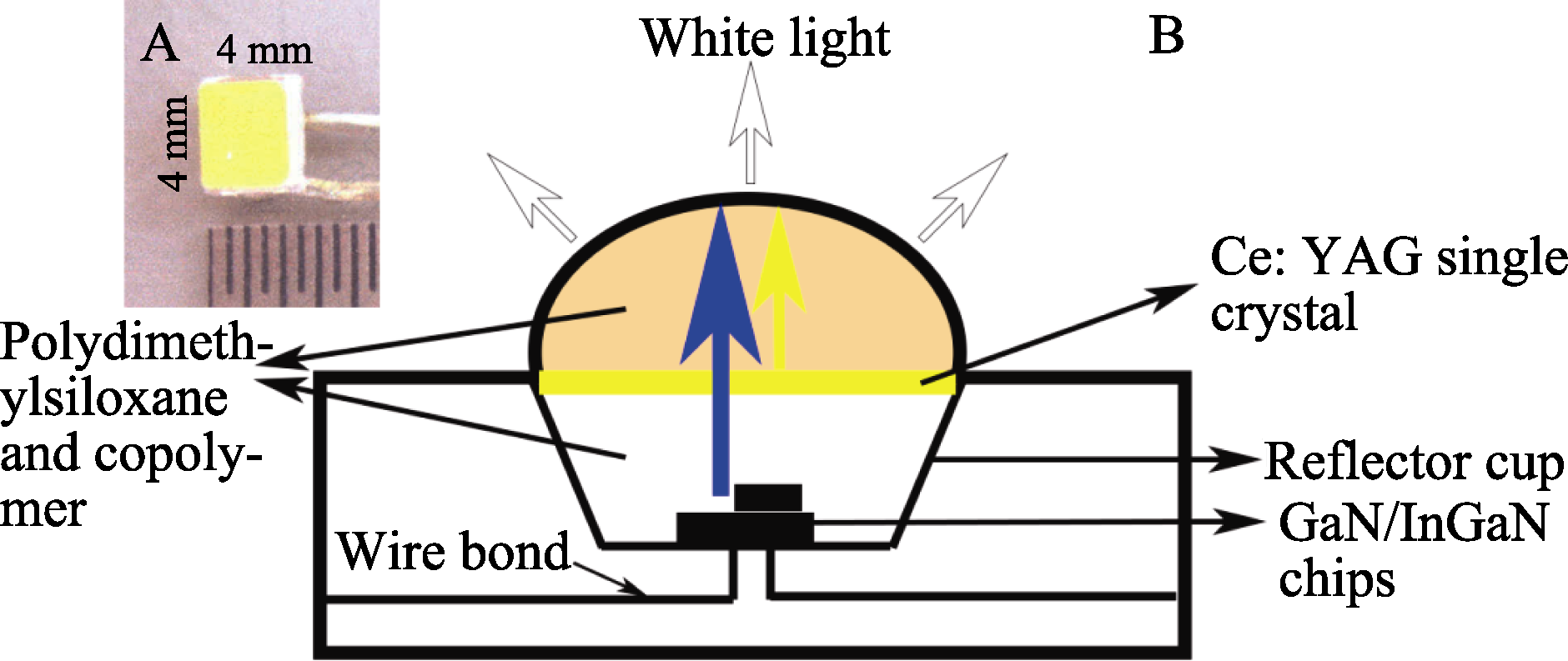
图1 Ce:YAG单晶制成的白光LED光源(A)和Ce:YAG单晶制得白光LED的封装结构(B)
Fig. 1 A sample of WLED fabricated by Ce:YAG single crystal (A) and Package structure of Ce:YAG single crystal for WLED (B)
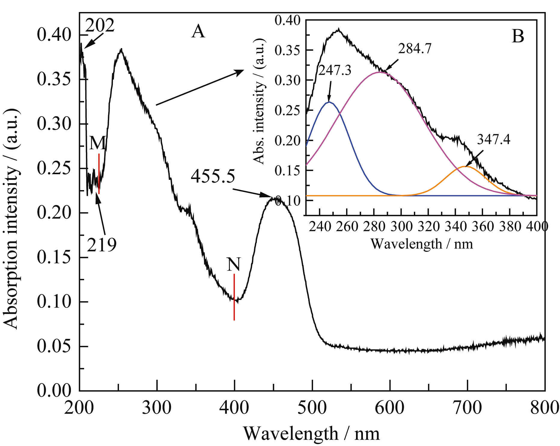
图2 Ce:YAG单晶的吸收光谱(A)和插图为MN段谱线用Lorentzian和Gaussian函数分峰拟合的结果(B)
Fig. 2 The absorption spectrum of Ce:YAG single crystal (A) and The inset shows the typical emission of spectrum in MN band separated into Lorentzian and Gaussian distributions (B)
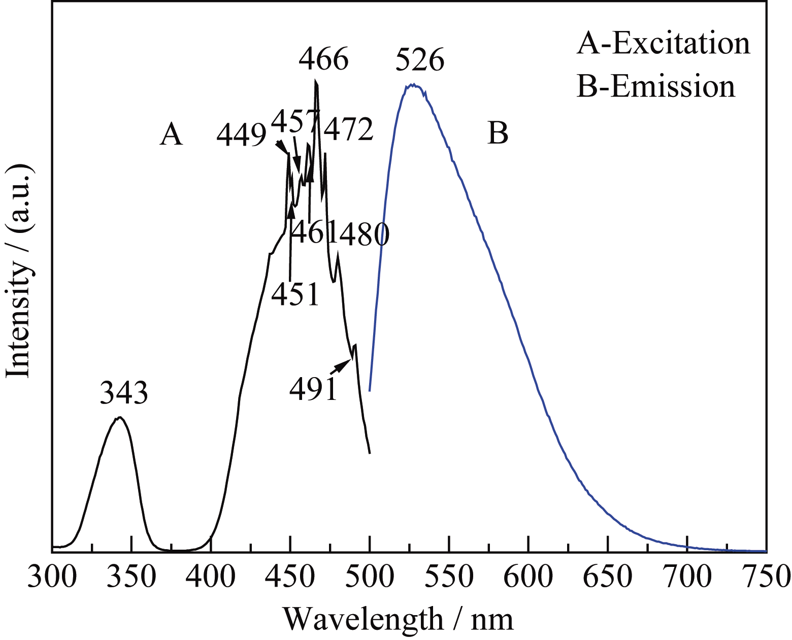
图3 Ce:YAG单晶的激发光谱(A)和发射光谱(B)
Fig. 3 Excitation (A) and emission (B) spectra of Ce:YAG single crystal
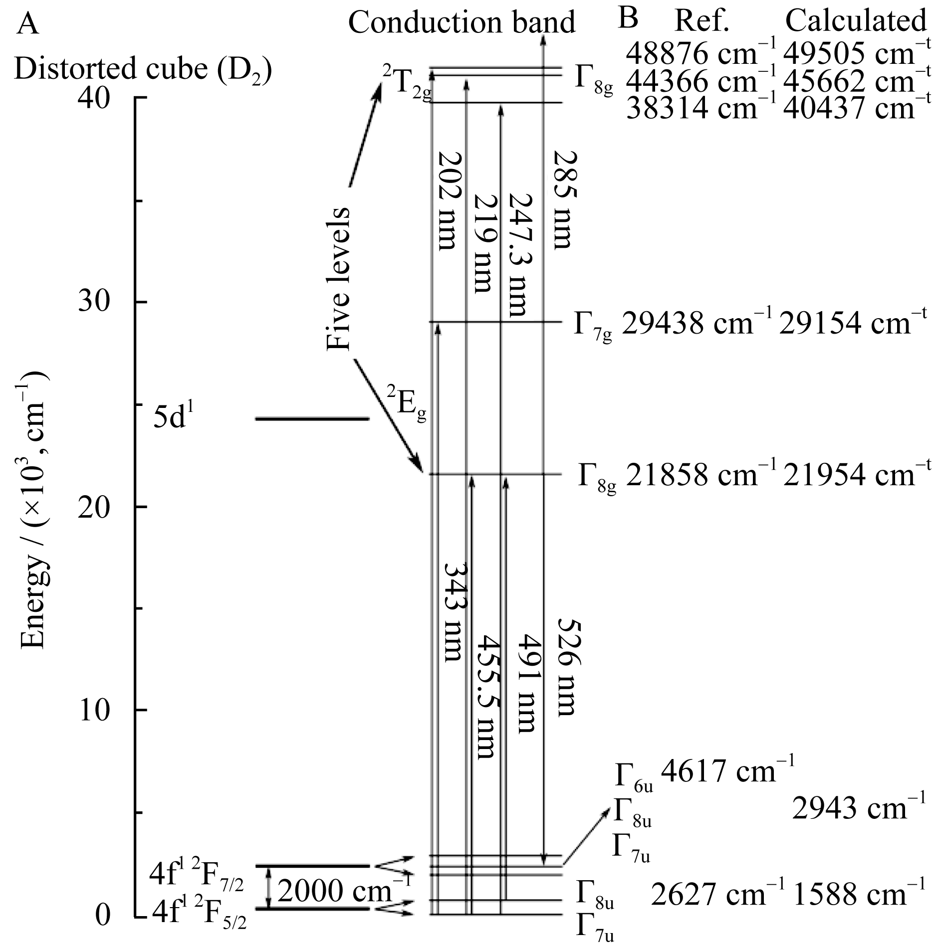
图4 Ce:YAG单晶中Ce3+4f和5d的Schematic能级图(A)和Ce3+4f和5d能级的文献值和实验计算值的比较(B)
Fig. 4 Schematic diagram of the energy level and band structure of the 4f and 5d configurations of the Ce3+ ion in a Ce:YAG single crystal field (A) and comparation between the literature values and experimental values of cerium 4f and 5d energy levels (B)
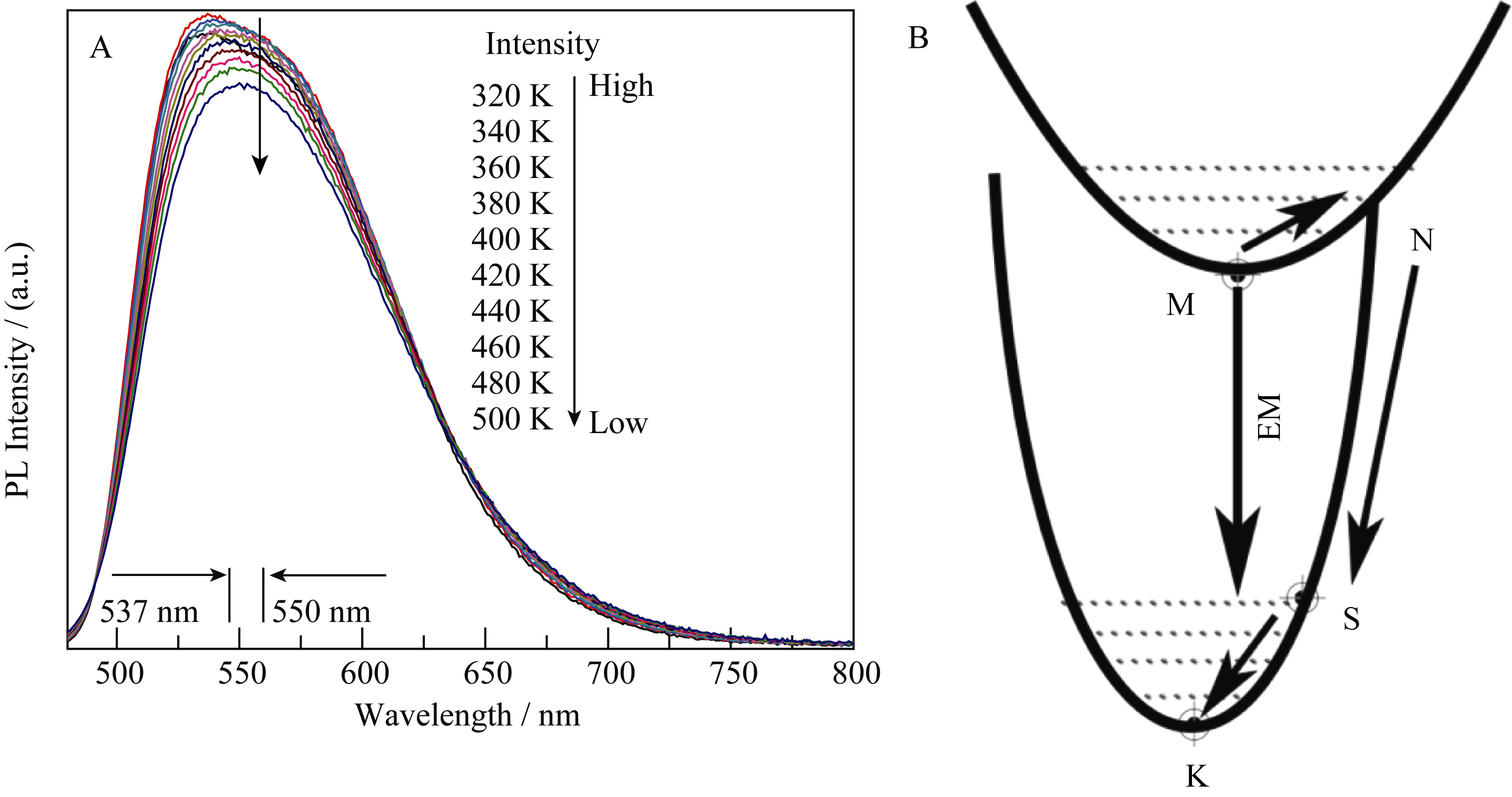
图5 Ce:YAG单晶的变温发光光谱(A)和Ce3+的无辐射跃迁过程(B)
Fig. 5 Temperature-dependent PL spectra of Ce:YAG single crystal (A) and A schematic illustration of nonradiative transition (B)
| Samples | Current<br/>/mA | Luminous flux<br/>/lm | Luminous efficacy<br/>/(lm•W-1) | Colour coordinate (x,y) | Colour temperature<br/>/K | Colour-rendering index |
|---|---|---|---|---|---|---|
| M1 chip | 60 | 2.687 | 13.995 | 0.1540,0.0240 | 1682 | 0 |
| M2 chip | 3.513 | 18.071 | 0.1528,0.0268 | 1665 | 0 | |
| M1 chip covered with<br/>epoxy glue | 3.689 | 19.898 | 0.1552,0.0331 | 1649 | 0 | |
| M2 chip covered with<br/>epoxy glue | 3.714 | 18.533 | 0.1551,0.0299 | 1661 | 0 |
表1 不同芯片的光电参数
Table 1 Photoelectric parameters of different chips
| Samples | Current<br/>/mA | Luminous flux<br/>/lm | Luminous efficacy<br/>/(lm•W-1) | Colour coordinate (x,y) | Colour temperature<br/>/K | Colour-rendering index |
|---|---|---|---|---|---|---|
| M1 chip | 60 | 2.687 | 13.995 | 0.1540,0.0240 | 1682 | 0 |
| M2 chip | 3.513 | 18.071 | 0.1528,0.0268 | 1665 | 0 | |
| M1 chip covered with<br/>epoxy glue | 3.689 | 19.898 | 0.1552,0.0331 | 1649 | 0 | |
| M2 chip covered with<br/>epoxy glue | 3.714 | 18.533 | 0.1551,0.0299 | 1661 | 0 |
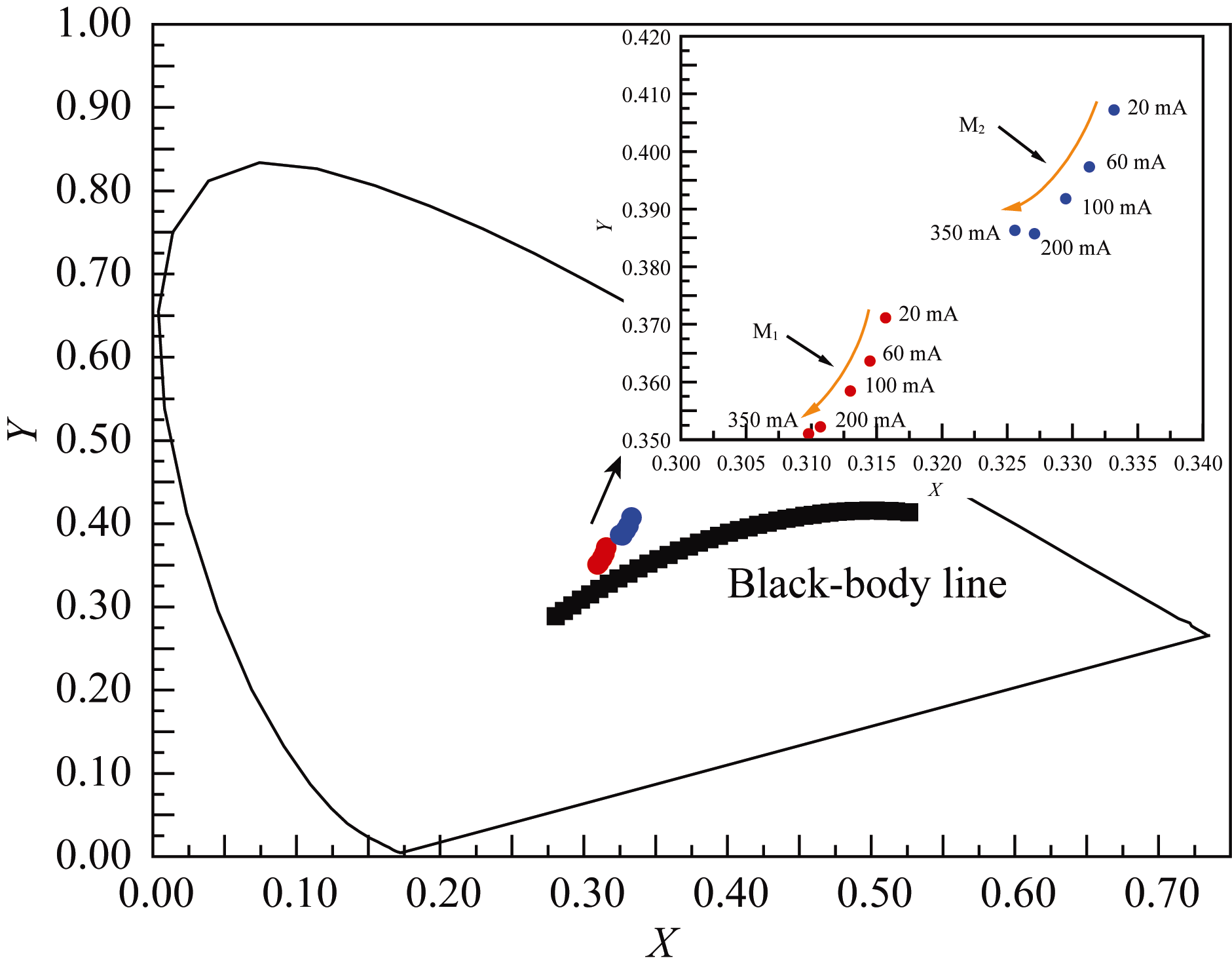
图6 Ce:YAG单晶制白光LED用不同芯片在变化的驱动电流下的色坐标
Fig. 6 Colour coordinates of WLEDs fabricated by the Ce: YAG single crystal (z=0.04) and different chips under changeable currents The inset obviously shows the changeable tendency of colour coordinates of WLEDs fabricated by the Ce:YAG single crystal (z=0.04) and different chips under different currents
| Samples | Thick-ness<br/>/mm | Current<br/>/mA | Luminous efficacy<br/>/(lm•W-1) | Colour coordinate<br/>(x,y) | Colour temperature<br/>/K | Colour-rendering index |
|---|---|---|---|---|---|---|
| WLEDs fabricated by the Ce:YAG single crystal (z=0.04) and M1 chip | 0.5 | 20 | 149.028 | 0.3157,0.3711 | 6148 | 66.4 |
| 60 | 121.466 | 0.3145,0.3636 | 6225 | 67.0 | ||
| 100 | 101.316 | 0.3130,0.3584 | 6316 | 67.4 | ||
| 200 | 69.415 | 0.3107,0.3522 | 6453 | 67.7 | ||
| 350 | 48.643 | 0.3098,0.3510 | 6501 | 68.3 | ||
| WLEDs fabricated by the Ce:YAG single crystal (z=0.04) and M2 chip | 20 | 138.617 | 0.3332,0.4072 | 5484 | 63.7 | |
| 60 | 117.950 | 0.3313,0.3973 | 5543 | 64.8 | ||
| 100 | 103.093 | 0.3295,0.3918 | 5603 | 65.5 | ||
| 200 | 68.295 | 0.3271,0.3857 | 5689 | 66.1 | ||
| 350 | 47.530 | 0.3256,0.3863 | 5743 | 67.3 |
表2 Ce:YAG单晶制白光LED在不同的驱动电流下的光电参数
Table 2 Photoelectric parameters of WLEDs fabricated by the Ce:YAG single crystal (z=0.04) under changeable currents
| Samples | Thick-ness<br/>/mm | Current<br/>/mA | Luminous efficacy<br/>/(lm•W-1) | Colour coordinate<br/>(x,y) | Colour temperature<br/>/K | Colour-rendering index |
|---|---|---|---|---|---|---|
| WLEDs fabricated by the Ce:YAG single crystal (z=0.04) and M1 chip | 0.5 | 20 | 149.028 | 0.3157,0.3711 | 6148 | 66.4 |
| 60 | 121.466 | 0.3145,0.3636 | 6225 | 67.0 | ||
| 100 | 101.316 | 0.3130,0.3584 | 6316 | 67.4 | ||
| 200 | 69.415 | 0.3107,0.3522 | 6453 | 67.7 | ||
| 350 | 48.643 | 0.3098,0.3510 | 6501 | 68.3 | ||
| WLEDs fabricated by the Ce:YAG single crystal (z=0.04) and M2 chip | 20 | 138.617 | 0.3332,0.4072 | 5484 | 63.7 | |
| 60 | 117.950 | 0.3313,0.3973 | 5543 | 64.8 | ||
| 100 | 103.093 | 0.3295,0.3918 | 5603 | 65.5 | ||
| 200 | 68.295 | 0.3271,0.3857 | 5689 | 66.1 | ||
| 350 | 47.530 | 0.3256,0.3863 | 5743 | 67.3 |
| Samples | Thickness<br/>/mm | Current<br/>/mA | Luminous efficacy<br/>/(lm•W-1) | Colour coordinate <br/>(x,y) | Colour temperature<br/>/K | Colour-rendering index |
|---|---|---|---|---|---|---|
| WLEDs fabricated <br/>by the Ce:YAG single crystal (z=0.04) <br/>and M2 chip | 0.4 | 60 | 76.744 | 0.2641,0.2580 | 15424 | 75.3 |
| 0.5 | 91.082 | 0.3362,0.4113 | 5395 | 64.3 | ||
| 1 | 91.748 | 0.3796,0.4934 | 4547 | 60.0 | ||
| 1.5 | 84.435 | 0.3772,0.4853 | 4570 | 60.7 |
表3 Ce:YAG单晶制白光LED在不同晶片厚度下的光电参数
Table 3 Photoelectric parameters of WLEDs fabricated by the Ce:YAG single crystal (z=0.04) with different thicknesses
| Samples | Thickness<br/>/mm | Current<br/>/mA | Luminous efficacy<br/>/(lm•W-1) | Colour coordinate <br/>(x,y) | Colour temperature<br/>/K | Colour-rendering index |
|---|---|---|---|---|---|---|
| WLEDs fabricated <br/>by the Ce:YAG single crystal (z=0.04) <br/>and M2 chip | 0.4 | 60 | 76.744 | 0.2641,0.2580 | 15424 | 75.3 |
| 0.5 | 91.082 | 0.3362,0.4113 | 5395 | 64.3 | ||
| 1 | 91.748 | 0.3796,0.4934 | 4547 | 60.0 | ||
| 1.5 | 84.435 | 0.3772,0.4853 | 4570 | 60.7 |
| Samples | Thickness<br/>/mm | Current<br/>/mA | Luminous efficacy<br/>/(lm•W-1) | Colour coordinate<br/>(x,y) | Colour temperature<br/>/K | Colour-rendering index |
|---|---|---|---|---|---|---|
| 1:0.01* | 0.5 | 60 | 107.765 | 0.3278,0.3442 | 5703 | 74.4 |
| 1:0.02* | 102.950 | 0.3378,0.3427 | 5272 | 77.7 |
表4 Ce:YAG单晶制白光LED中添加红粉的光电参数
Table 4 Photoelectric parameters of WLEDs fabricated by the Ce:YAG single crystal (z=0.04) and red phosphors
| Samples | Thickness<br/>/mm | Current<br/>/mA | Luminous efficacy<br/>/(lm•W-1) | Colour coordinate<br/>(x,y) | Colour temperature<br/>/K | Colour-rendering index |
|---|---|---|---|---|---|---|
| 1:0.01* | 0.5 | 60 | 107.765 | 0.3278,0.3442 | 5703 | 74.4 |
| 1:0.02* | 102.950 | 0.3378,0.3427 | 5272 | 77.7 |
| Samples | Thickness<br/>/mm | Current<br/>/mA | Luminous efficacy<br/>/(lm•W-1) | Colour coordinate<br/>(x,y) | Colour temperature<br/>/K | Colour-rendering index |
|---|---|---|---|---|---|---|
| WLEDs fabricated by Ce:YAG single crystal (z=0.04) | 0.5 | 60 | 107.297 | 0.3488,0.3580 | 4862 | 81.9 |
| Warm-WLEDs fabricated <br/>by phosphors | - | 103.180 | 0.3938,0.3850 | 3730 | 74.0 |
表5 Ce:YAG单晶制白光LED光源和商业白光LED的光电参数
Table 5 Photoelectric parameters of WLEDs fabricated by eithor Ce:YAG single crystal (z=0.04) or commercial phosphors
| Samples | Thickness<br/>/mm | Current<br/>/mA | Luminous efficacy<br/>/(lm•W-1) | Colour coordinate<br/>(x,y) | Colour temperature<br/>/K | Colour-rendering index |
|---|---|---|---|---|---|---|
| WLEDs fabricated by Ce:YAG single crystal (z=0.04) | 0.5 | 60 | 107.297 | 0.3488,0.3580 | 4862 | 81.9 |
| Warm-WLEDs fabricated <br/>by phosphors | - | 103.180 | 0.3938,0.3850 | 3730 | 74.0 |
| [1] | ZHANG S, LI C, PANG R, et al. Long-lasting phosphorescence study on Y3Al5O12 doped with different concentrations of Ce3+. J. Rare Earths, 2011, 29(5): 426-430. |
| [2] | MIHÓKOVÁ E, NIKL M, MAREŠ J A, et al. Luminescence and scintillation properties of YAG:Ce single crystal and optical ceramics. J. Lumin., 2007, 126(1): 77-80. |
| [3] | KAMADA K, YANAGIDA T, TSUTSUMI K, et al. Scintillation properties of 2inch-diameter Pr:Lu3Al5O12 (LuAG) single crystal. IEEE Trans. Nucl. Sci., 2009, 56(3): 570-573. |
| [4] | CLAUSEN C, USMANI I, BUSSIÈRES F, et al. Quantum storage of photonic entanglement in a crystal. Nature, 2011, 469(7331): 508-511. |
| [5] | KATSUMATA T. Recent Progress in Sensor Materials for Fluorescence Thermometry. ICCAS, International Conference on Control, Automation and Systems, 14-17 Oct, 2008: 2748-2751. |
| [6] | KOLESOV R, XIA K, REUTER R, et al. Optical detection of a single rare-earth ion in a crystal. Nat. Commun , 2012, 3: 1029-1-7. |
| [7] | WUISTER S F, DONEGA C D M, MEIJERINK A. Efficient energy transfer between nanocrystalline YAG:Ce and TRITC. Phys. Chem. Chem. Phys., 2004, 6(8): 1633-1636. |
| [8] | PIMPUTKAR S, SPECK J S, DENBAARS S P, et al. Prospects for LED lighting. Nat. Photonics, 2009, 3(4): 180-182. |
| [9] | ALLEN S C, STECKL A J. A nearly ideal phosphor-converted white light-emitting diode. Appl. Phys. Lett. , 2008, 92(14): 143309-1-3. |
| [10] | NAKAMURA S, FASOL G. The Blue Laser Diode: The Complete Story. Berlin: Springer, 1997: 216. |
| [11] | ZHANG X, LIU Y, HAO Z, et al. Yellow-emitting (Ca2Lu1-xCex) (ScMg)Si3O12 phosphor and its application for white LEDs. Mater. Res. Bull., 2012, 47(5): 1149-1152. |
| [12] | KRAMES M R, SHCHEKIN O B, MUELLER-MACH R, et al. Status and future of high-power light-emitting diodes for solid-state lighting. J. Display Techn., 2007, 3(2): 160-175. |
| [13] | LATYNINA A, WATANABE M, INOMATA D, et al. Properties of Czochralski grown Ce,Gd:Y3Al5O12 single crystal for white light-emitting diode. J. Alloys Compd., 2013, 553: 89-92. |
| [14] | NARENDRAN N, GU Y, FREYSSINIER J P, et al. Solid-state lighting: failure analysis of white LEDs. J. Cryst. Growth, 2004, 268(3/4): 449-456. |
| [15] | MUÑOZ-GARCÍA A B, SEIJO L. Ce and La single- and double- substitutional defects in yttrium aluminum garnet: first-principles study. J. Phys. Chem. A, 2011, 115(5): 815-823. |
| [16] | LU S Z, YANG Q H, XU F, et al. Investigation of white light emitting diode based on Ce:YAG single crystal. Acta. Opt. Sinica, 2012, 32(3): 0323001-1-6. |
| [17] | TANNER P, FU L, NING L, et al. Soft synthesis and vacuum ultraviolet spectra of YAG:Ce3+ nanocrystals: reassignment of Ce3+ energy levels. J. Phys.: Condens. Matter, 2007, 19(21): 216213-1-14. |
| [18] | OWEN J F, DORAIN P B, KOBAYASHI T. Excited-state absorption in Eu+2: CaF2 and Ce+3: YAG single crystals at 298 and 77 K. J. Appl. Phys., 1981, 52(3): 1216-1223. |
| [19] | TANNER P A, MAK C S K, EDELSTEIN N M, et al. Absorption and emission spectra of Ce3+ in elpasolite lattices. J. Am. Chem. Soc., 2003, 125(43): 13225-13233. |
| [20] | OGIEGLO J M, ZYCH A, IVANOVSKIKH K V, et al. Luminescence and energy transfer in Lu3Al5O12 scintillators co-doped with Ce3+ and Tb3+. J. Phys. Chem. A, 2012, 116(33): 8464-8474. |
| [21] | BACHMANN V, RONDA C, MEIJERINK A. Temperature quenching of yellow Ce3+ luminescence in YAG:Ce. Chem. Mater., 2009, 21(10): 2077-2084. |
| [22] | SETLUR A A, SRIVASTAVA A M. On the relationship between emission color and Ce3+ concentration in garnet phosphors .Opt. Mater., 2006, 29(12): 1647-1652. |
| [23] | TOMIKI T, KOHATSU T, SHIMABUKURO H, et al. Ce3+ centres in Y3Al5O12 (YAG) single crystals II. J. Phys. Soc. Japan, 1992, 61: 2382-2387. |
| [24] | REYHER H J, HAUSFELD N, PAPE M, et al. Attribution of the near-UV absorption bands of YAG:Ce to Ce3+-ions by MCD and ODMR .Solid State Commun., 1999, 110(6): 345-349. |
| [25] | JAYAWARDENA A, LIU Y, NARENDRAN N. Analysis of three different junction temperature estimation methods for AC LEDs. Solid-State Electron, 2013, 86: 11-16. |
| [26] | XIE R J, HIROSAKI N. Silicon-based oxynitride and nitride phosphors for white LEDs—A review. Sci. Technol. Adv. Mater., 2007, 8(7/8): 588-600. |
| [27] | SETLUR A A, HEWARD W J, HANNAH M E, et al. Incorporation of Si4+-N3- into Ce3+ -doped garnets for warm white LED phosphors. Chem. Mater., 2008, 20(19): 6277-6283. |
| [28] | MORELLO G, GIORGI M D, KUDERA S, et al. Temperature and size dependence of nonradiative relaxation and exciton- phonon coupling in colloidal CdTe quantum dots. J. Phys. Chem. C, 2007, 111(16): 5846-5849. |
| [29] | JING P T, ZHENG J J, IKEZAWA M, et al. Temperature-dependent photoluminescence of CdSe-core CdS/CdZnS/ ZnS-multishell quantum dots. J. Phys. Chem. C, 2009, 113(31): 13545-13550. |
| [30] | SHI A, WANG X, MENG X, et al. Temperature-dependent photoluminescence of CuInS2 quantum dots. J. Lumin., 2012, 132(7): 1819-1823. |
| [31] | YE S, XIAO F, PAN Y X, et al. Phosphors in phosphor-converted white light-emitting diodes: recent advances in materials, techniques and properties. Mater. Sci. Eng. R, 2010, 71(1): 1-34. |
| [32] | ZYCH E, BRECHER C, GLODO J. Kinetics of cerium emission in a YAG:Ce single crystal: the role of traps. J. Phys.: Condens. Matter, 2000, 12(8): 1947-1958. |
| [33] | ZHAN X. White Light Emitting diode (WLED) and Packing Method Thereof. United States , US7655487 B2.Jun. 25, 2009. |
| [34] | GB/T 24908-2010, Self-ballasted LED Lamps for General Lighting Services-performance Requirements.B/T 24908-2010, Self-ballasted LED Lamps for General Lighting Services-performance Requirements. |
| [1] | 王瑜, 刘欣, 王艳香, 李家科. ZnFe2O4//rGH水系光辅助充电超级电容器的构建与性能研究[J]. 无机材料学报, 2026, 41(1): 79-86. |
| [2] | 韩伟伟, 黄东, 李廷松, 李江. 包边复合结构Sm:LuAG/Nd:LuAG激光陶瓷的制备及性能研究[J]. 无机材料学报, 2026, 41(1): 113-118. |
| [3] | 潘泽晟, 游雅萍, 郑雅, 陈海杰, 王连军, 江莞. 面向紫光激发白光LED用荧光材料的耐候性[J]. 无机材料学报, 2025, 40(3): 314-322. |
| [4] | 叶君豪, 周真真, 胡辰, 王雁斌, 荆延秋, 李廷松, 程梓秋, 吴俊林, IVANOV Maxim, HRENIAK Dariusz, 李江. 共沉淀纳米粉体制备Yb:Sc2O3透明陶瓷的微结构与光学性能[J]. 无机材料学报, 2025, 40(2): 215-224. |
| [5] | 瞿牡静, 张淑兰, 朱梦梦, 丁浩杰, 段嘉欣, 代恒龙, 周国红, 李会利. CsPbBr3@MIL-53纳米复合荧光粉的合成、性能及其白光LEDs应用[J]. 无机材料学报, 2024, 39(9): 1035-1043. |
| [6] | 吕朝阳, 徐勇, 杨久延, 涂广升, 涂兵田, 王皓. MgF2助剂对MgAl1.9Ga0.1O4透明陶瓷的制备与光学性能的影响[J]. 无机材料学报, 2024, 39(5): 531-538. |
| [7] | 费玲, 雷蕾, 汪德高. 二维MXene材料在新型薄膜太阳能电池技术中的研究进展[J]. 无机材料学报, 2024, 39(2): 215-224. |
| [8] | 顾军毅, 范武刚, 张兆泉, 姚琴, 展红全. 还原制备Pr2O3粉体及其结构和光学性能研究[J]. 无机材料学报, 2023, 38(7): 771-777. |
| [9] | 李悦, 张旭良, 景芳丽, 胡章贵, 吴以成. 铈掺杂硼酸钙镧晶体的生长与性能研究[J]. 无机材料学报, 2023, 38(5): 583-588. |
| [10] | 王海东, 王燕, 朱昭捷, 李坚富, LAKSHMINARAYANA Gandham, 涂朝阳. Dy3+掺杂SrGdGa3O7晶体的晶体生长, 结构、光学和可见光荧光特性[J]. 无机材料学报, 2023, 38(12): 1475-1482. |
| [11] | 陆晨辉, 葛万银, 宋盼盼, 张盼锋, 徐美美, 张伟. 用于白光LED稀土Eu掺杂SiAlON基荧光粉的发光性能[J]. 无机材料学报, 2023, 38(1): 97-104. |
| [12] | 李文俊, 王皓, 涂兵田, 谌强国, 郑凯平, 王为民, 傅正义. 宽光谱透过Mg0.9Al2.08O3.97N0.03透明陶瓷的制备与性能研究[J]. 无机材料学报, 2022, 37(9): 969-975. |
| [13] | 刘强, 王倩, 陈鹏辉, 李晓英, 章立轩, 谢腾飞, 李江. 两步烧结法制备红色Ce:8YSZ透明陶瓷及其性能研究[J]. 无机材料学报, 2022, 37(8): 911-917. |
| [14] | 王兆武, 姬海鹏, 王飞翔, 侯星慧, 易莎莎, 周颖, 陈德良. 调控Al2O3晶型控制MgAl2O4:Mn4+荧光粉中Mn价态研究[J]. 无机材料学报, 2021, 36(5): 513-520. |
| [15] | 刘子玉, TOCI Guido, PIRRI Angela, PATRIZI Barbara, 冯亚刚, 陈肖朴, 胡殿君, 田丰, 吴乐翔, VANNINIMatteo, 李江. 固体激光用Nd:Lu2O3透明陶瓷的制备和光学性能研究[J]. 无机材料学报, 2021, 36(2): 210-216. |
| 阅读次数 | ||||||
|
全文 |
|
|||||
|
摘要 |
|
|||||