无机材料学报 ›› 2014, Vol. 29 ›› Issue (3): 225-236.DOI: 10.3724/SP.J.1077.2014.13170 CSTR: 32189.14.SP.J.1077.2014.13170
• • 下一篇
李建林1, 陈彬彬1, 章 文1, 王连军2, 江 莞2
收稿日期:2013-03-25
修回日期:2013-06-30
出版日期:2014-03-20
网络出版日期:2014-02-18
基金资助:LI Jian-Lin1, CHEN Bin-Bin1, ZHANG Wen1, WANG Lian-Jun2, JIANG Wan2
Received:2013-03-25
Revised:2013-06-30
Published:2014-03-20
Online:2014-02-18
Supported by:摘要:
石墨烯是2004年首次成功制备的新型二维碳纳米材料。由于其独特的二维结构和优异的性能, 近年来已成为国内外材料领域的研究热点。本文结合本课题组的相关工作, 综述了石墨烯应用于陶瓷块体复合材料的新近研究成果,包括碳纳米管、SiOC、Al2O3以及Si3N4等为基体的石墨烯块体复合材料,重点介绍了陶瓷/石墨烯块体复合材料的制备方法、增韧机制以及优异的物化性能, 并探讨了陶瓷/石墨烯块体复合材料的研究发展方向和应用前景。
中图分类号:
李建林, 陈彬彬, 章 文, 王连军, 江 莞. 陶瓷/石墨烯块体复合材料的研究进展[J]. 无机材料学报, 2014, 29(3): 225-236.
LI Jian-Lin, CHEN Bin-Bin, ZHANG Wen, WANG Lian-Jun, JIANG Wan. Recent Progress in Ceramic/Graphene Bulk Composites[J]. Journal of Inorganic Materials, 2014, 29(3): 225-236.
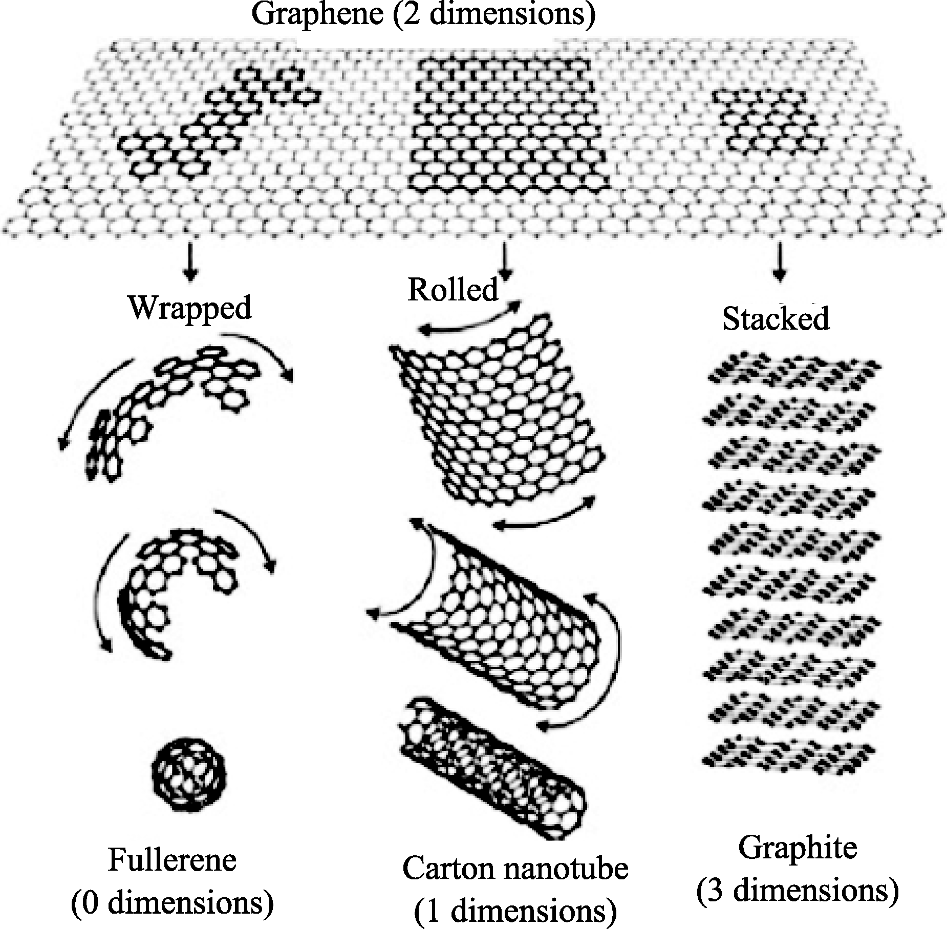
图1 单层石墨烯及其衍生物示意图[1]
Fig. 1 Schematic diagrams of graphene and its derivatives[1]
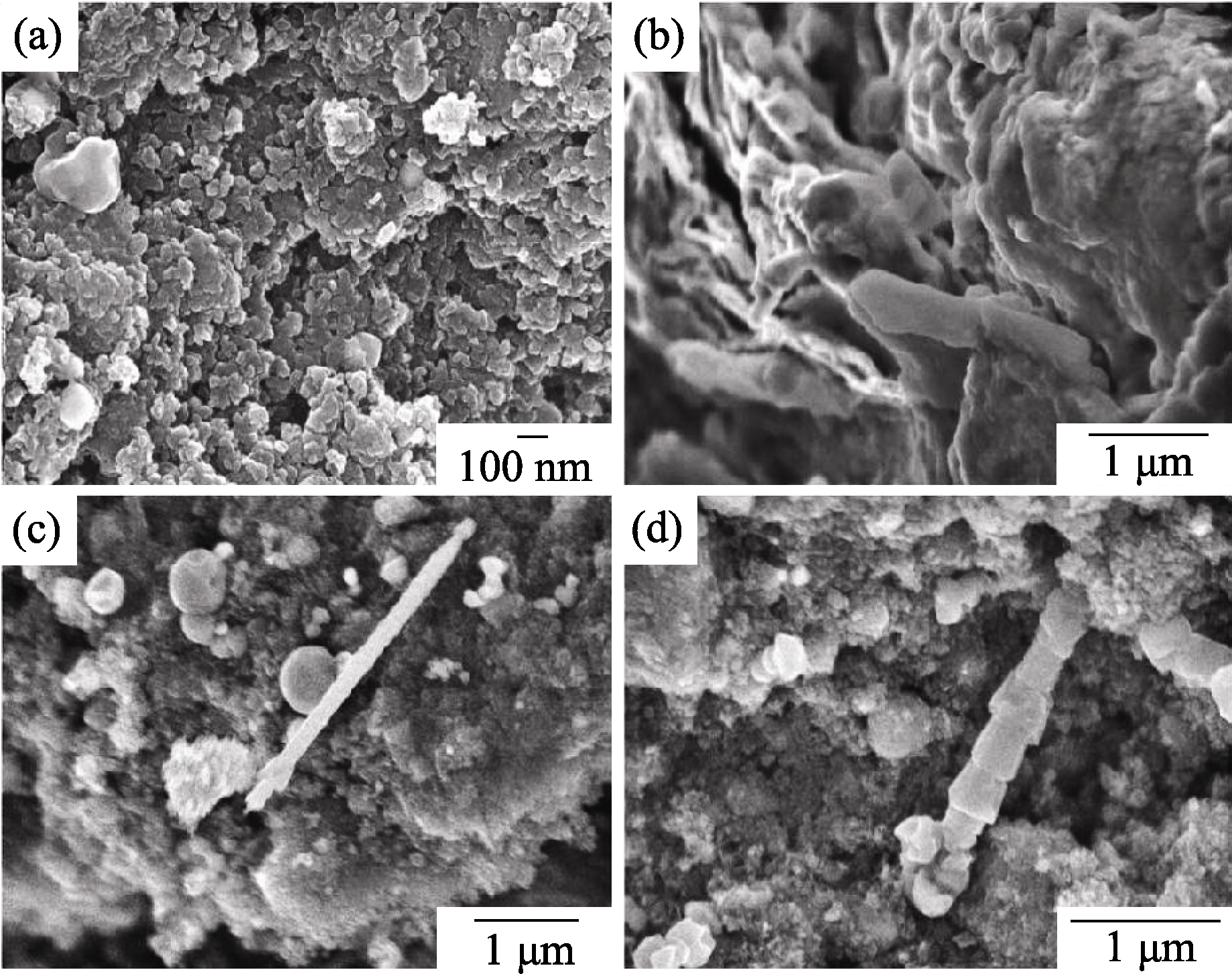
图2 球磨后的粉体FESEM照片
Fig. 2 FESEM micrographs of high energy ball milled graphite powder (a) As-milled graphite powder; (b) Graphite layers with a thickness of 20-50 nm that were highly distorted due to heavy impact of milling balls; (c) and (d) Carbon tubes with a diameter of 80-300 nm and a length of several microns produced during the milling[15]
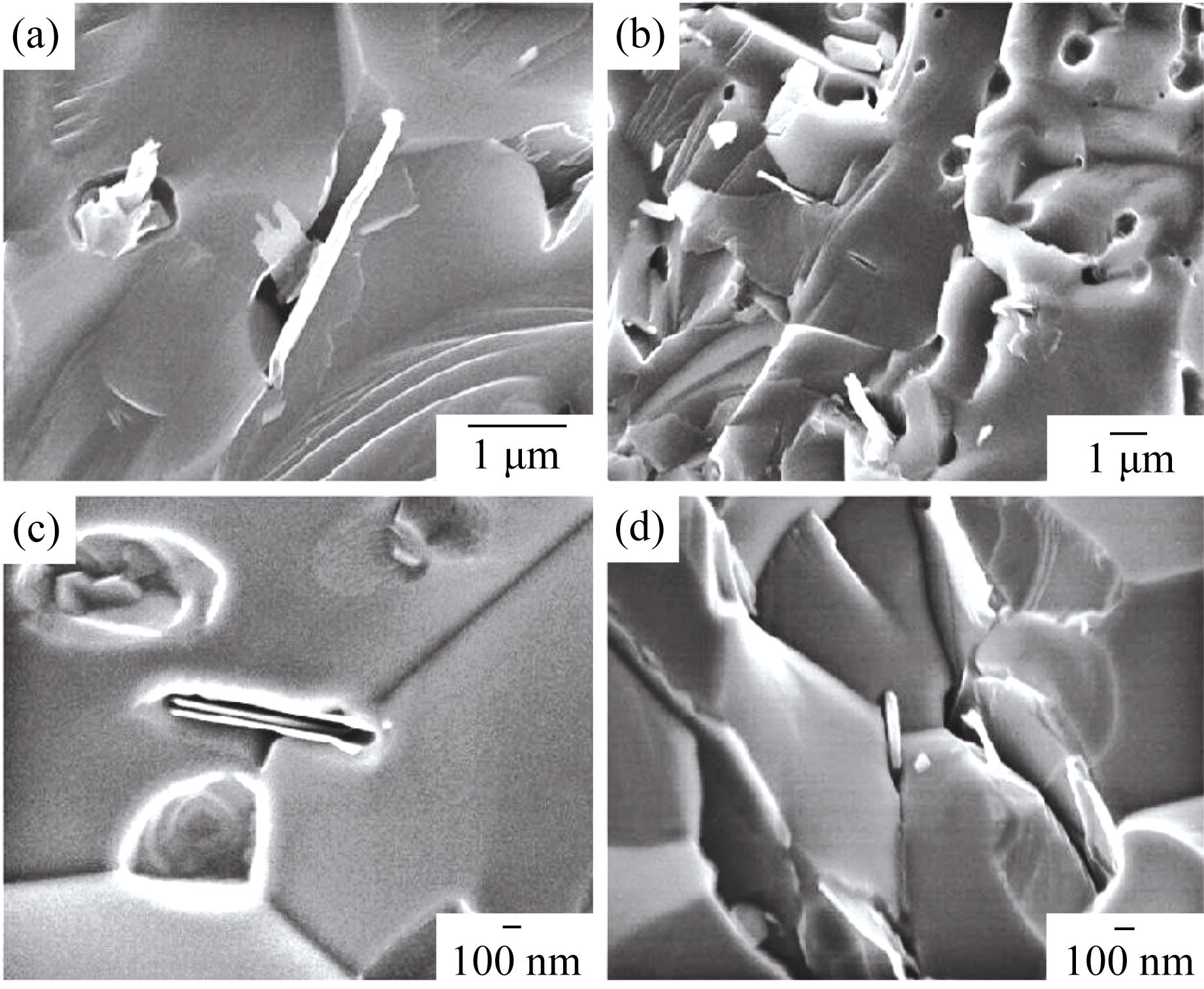
图3 TiC/C复合材料断面的FESEM照片, 展示了纳米尺寸的石墨烯片和碳管, 约15%的孔隙率, 且平均孔径为3 μm[15]
Fig. 3 FESEM micrographs showing nanosized graphene sheets and carbon tubes on fractured surface of TiC/C composite and pores of an average size of about 3 μm with a porosity of about 15%[15]

图4 FESEM照片: (a)未经处理的作为起始原料的多壁碳纳米管; (b)和(c)摩擦抛光后的多壁碳纳米管表面((b)一个由高密度聚集的碳纳米管构成的有光泽表面, (c)从密集到疏松过渡的碳纳米管); (d)摩擦抛光后的块体材料表面, 在表面的多壁碳纳米管结构已经发生改变, 外凸的石墨烯壁从碳管上脱落[16]
Fig. 4 FESEM micrographs showing: (a) the raw MWCNTs used as the starting material; (b-c) polished surface with a scratch of MWCNTs ((b) a shiny surface comprised of high- density aggregation CNTs; (c) transition from the dense to the loose CNTs); (d) polished surface with a scratch on it, MWCNTs in the surface have changed their structure and the outer graphene walls have come off the tubes[16]
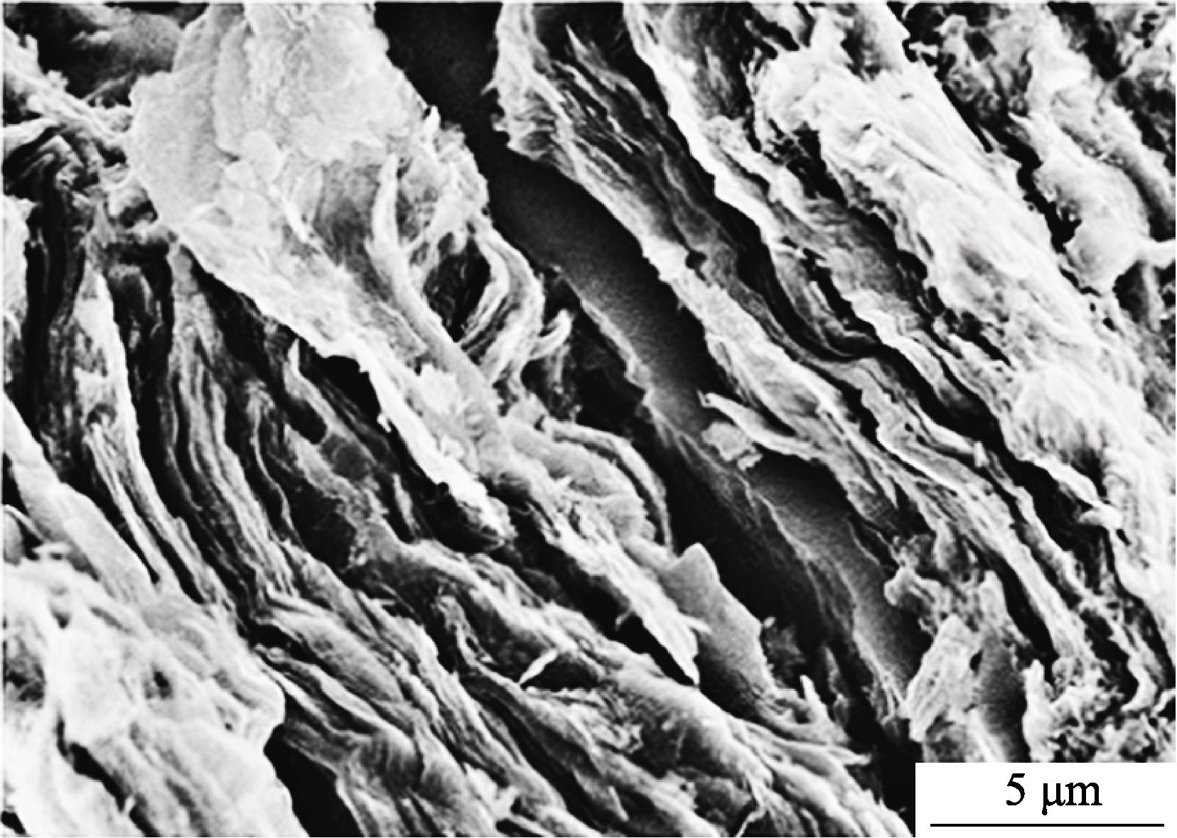
图5 SiOC/GNS 断面SEM照片, 石墨烯在陶瓷中形成片层状结构, 呈一定取向分布[20]
Fig.5 SEM image of the fracture surface of SiOC/GNS composite, with graphene forming a lamellar structure of a certain aligned distribution in the ceramic matrix[20]
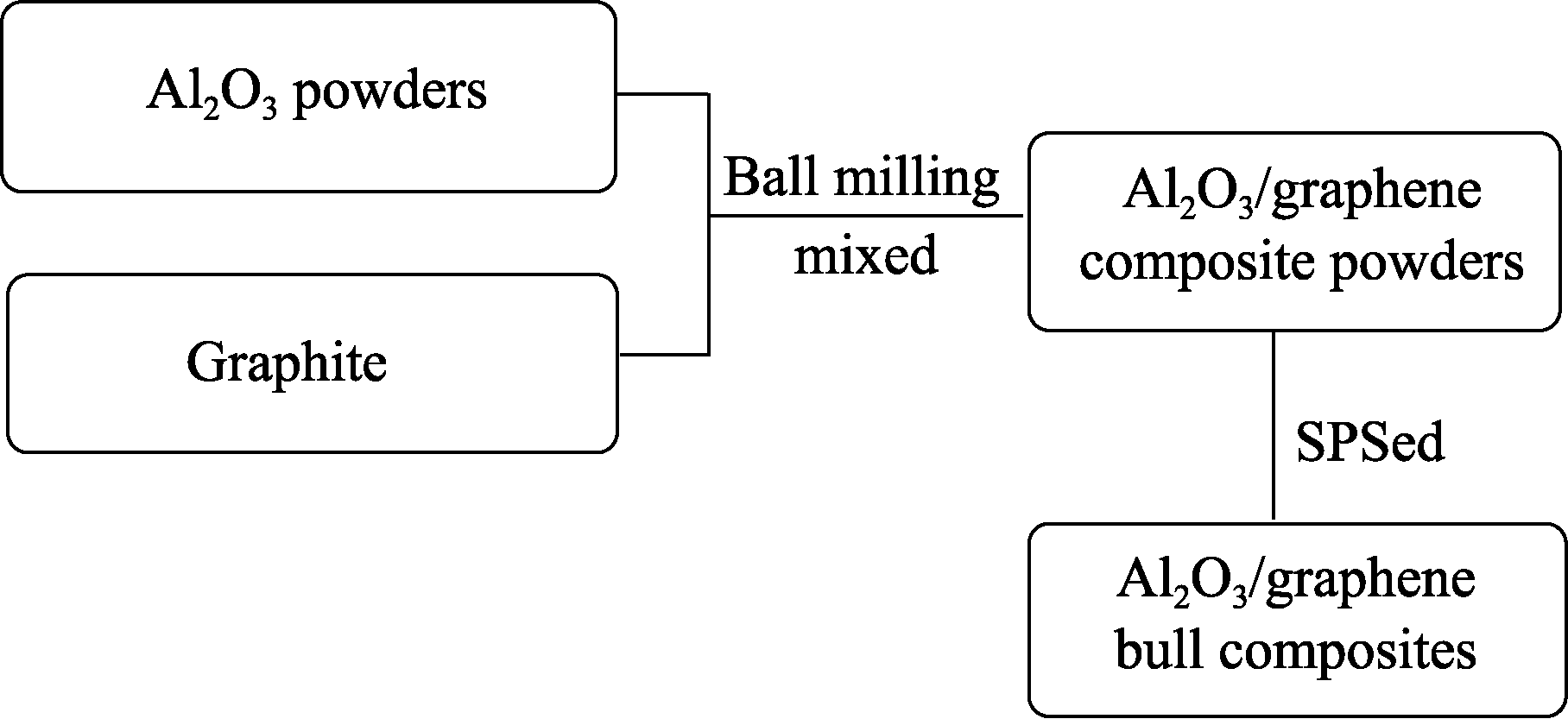
图6 Al2O3/石墨烯块体复合材料的制备过程示意图
Fig. 6 Schematic diagram of the preparation process of Al2O3/GNS bulk composites
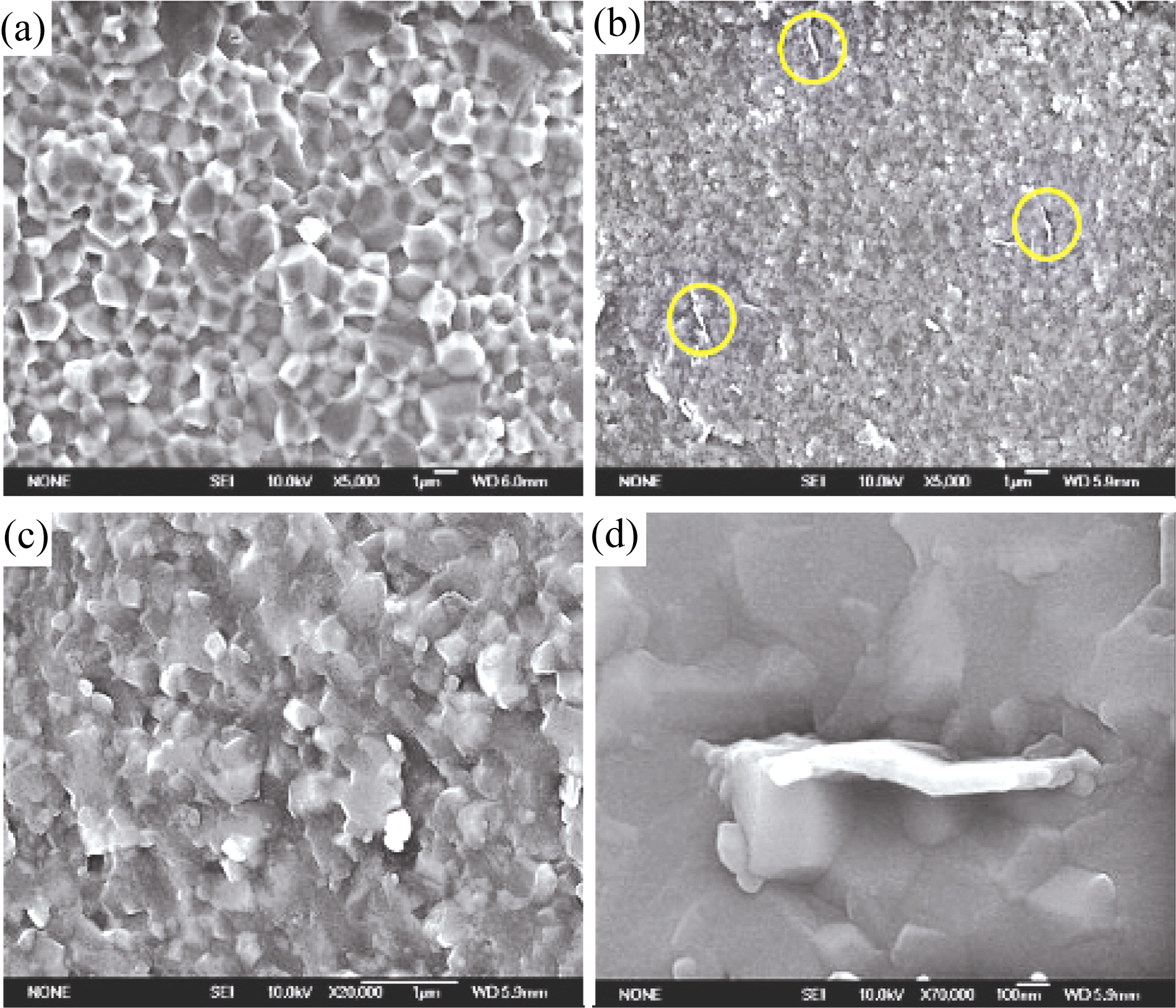
图 7 纯氧化铝陶瓷(a)及GNSs含量为 1vol%的GNS/ Al2O3复合材料(b~d)的断面SEM照片[22]
Fig. 7 SEM images of fractured surfaces of a pure Al2O3 ceramic (a) and a GNS/Al2O3 composite containing 1vol% GNSs (b-d) (c) and (d) are magnified parts of (b)[22]
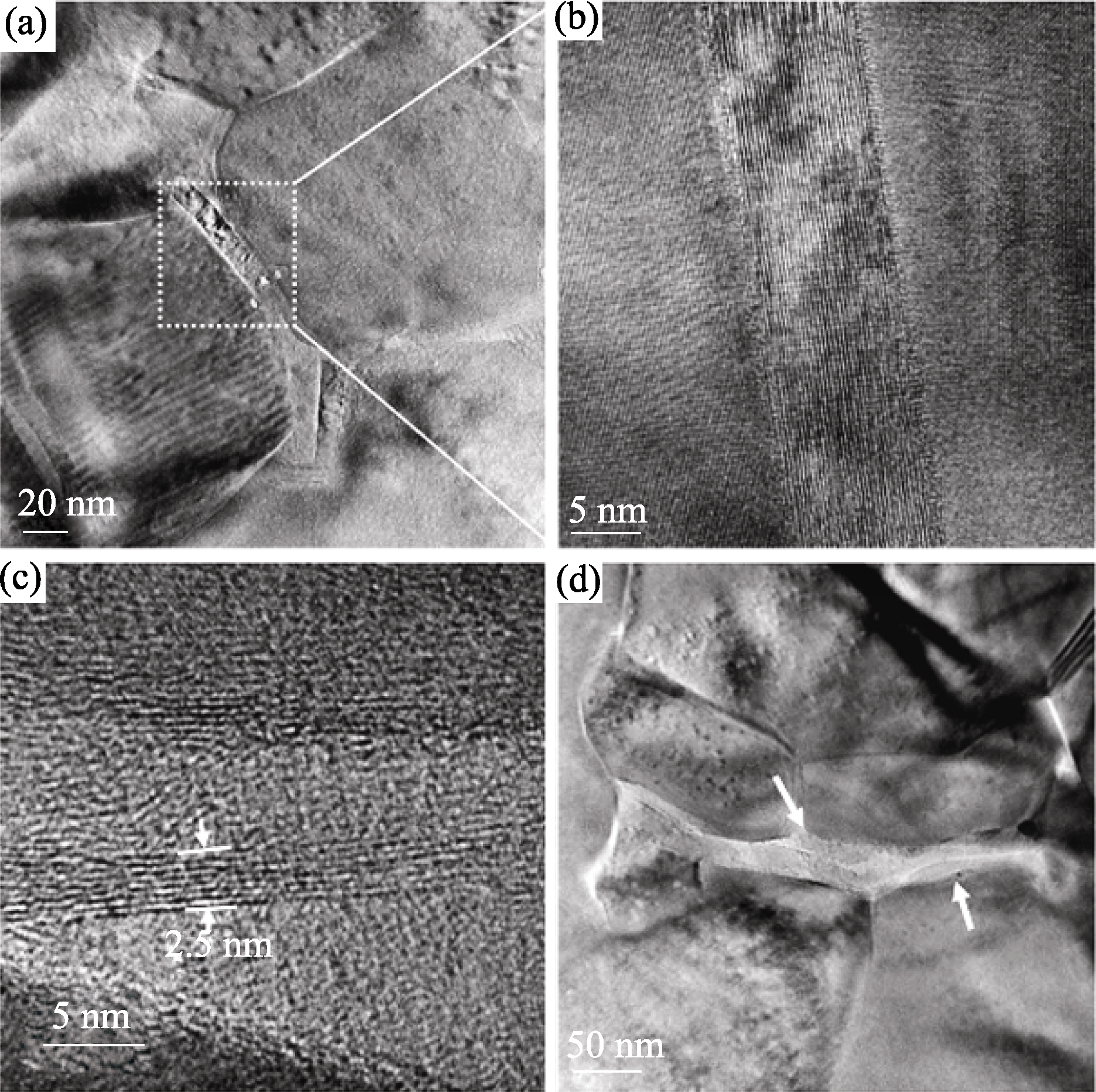
图 8 GNSs含量为 5vol%的GNS/Al2O3 复合材料的TEM和HRTEM照片
Fig. 8 TEM and HRTEM images of a GNS/Al2O3composite containing 5vol% GNSs (a) GNSs surrounding Al2O3 nanoparticles; (b) A magnified image of GNSs with a thickness of about 10 nm in (a); (c) GNSs with a thickness of 2.5 nm; (d) Overlap of GNSs between Al2O3 nano-particles[22]
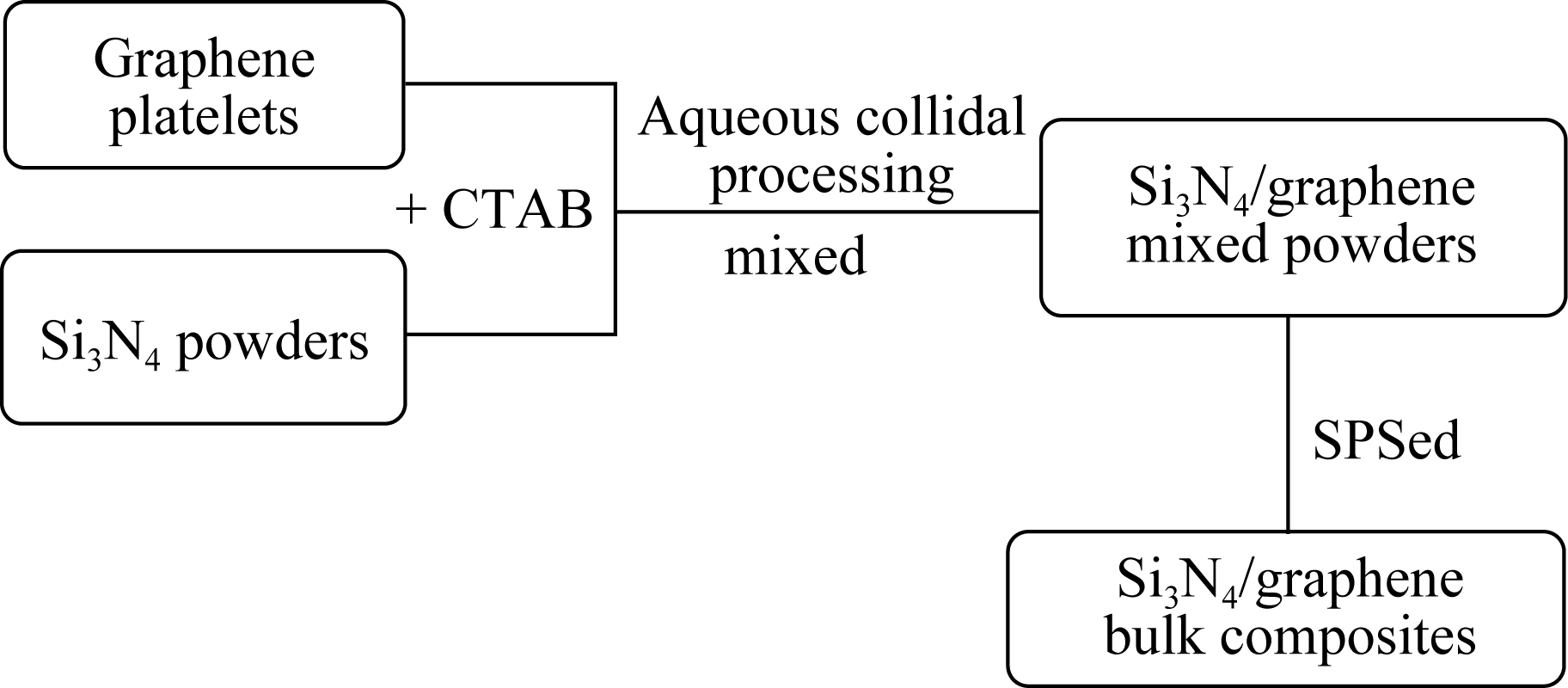
图9 Si3N4/石墨烯块体复合材料的制备示意图
Fig. 9 A proposed scheme of the fabbrication of Si3N4/graphene bulk composites
| Starting powders / wt% | Additives / wt% | Type of GPL additive | Hardness HV/GPa | Fracture toughness KIC/(MPa•m1/2) | ||
|---|---|---|---|---|---|---|
| Si3N4 | Al2O3 | Y2O3 | C | |||
| 90 | 4 | 6 | 1 | Multilayer graphene | 16.38 ± 0.48 | 9.92 ± 0.38 |
| 90 | 4 | 6 | 1 | Nanographene platelets:Angstron Noo6-010-P | 14.59 ± 0.43 | 8.89 ± 0.37 |
| 90 | 4 | 6 | 1 | Exfoliated graphene nanoplatelets xGnp-M-25 | 15.05 ± 0.31 | 8.62 ± 0.17 |
| 90 | 4 | 6 | 1 | Exfoliated graphene nanoplatelets xGnp-M-5 | 14.59 ± 0.25 | 7.84 ± 0.43 |
| 90 | 4 | 6 | 0 | - | 15.38 ± 0.48 | 6.89 ± 0.39 |
表1 不同Si3N4/石墨烯复合材料的力学性能[34]
Table 1 Mechanical properties of different Si3N4/graphene composites [34]
| Starting powders / wt% | Additives / wt% | Type of GPL additive | Hardness HV/GPa | Fracture toughness KIC/(MPa•m1/2) | ||
|---|---|---|---|---|---|---|
| Si3N4 | Al2O3 | Y2O3 | C | |||
| 90 | 4 | 6 | 1 | Multilayer graphene | 16.38 ± 0.48 | 9.92 ± 0.38 |
| 90 | 4 | 6 | 1 | Nanographene platelets:Angstron Noo6-010-P | 14.59 ± 0.43 | 8.89 ± 0.37 |
| 90 | 4 | 6 | 1 | Exfoliated graphene nanoplatelets xGnp-M-25 | 15.05 ± 0.31 | 8.62 ± 0.17 |
| 90 | 4 | 6 | 1 | Exfoliated graphene nanoplatelets xGnp-M-5 | 14.59 ± 0.25 | 7.84 ± 0.43 |
| 90 | 4 | 6 | 0 | - | 15.38 ± 0.48 | 6.89 ± 0.39 |
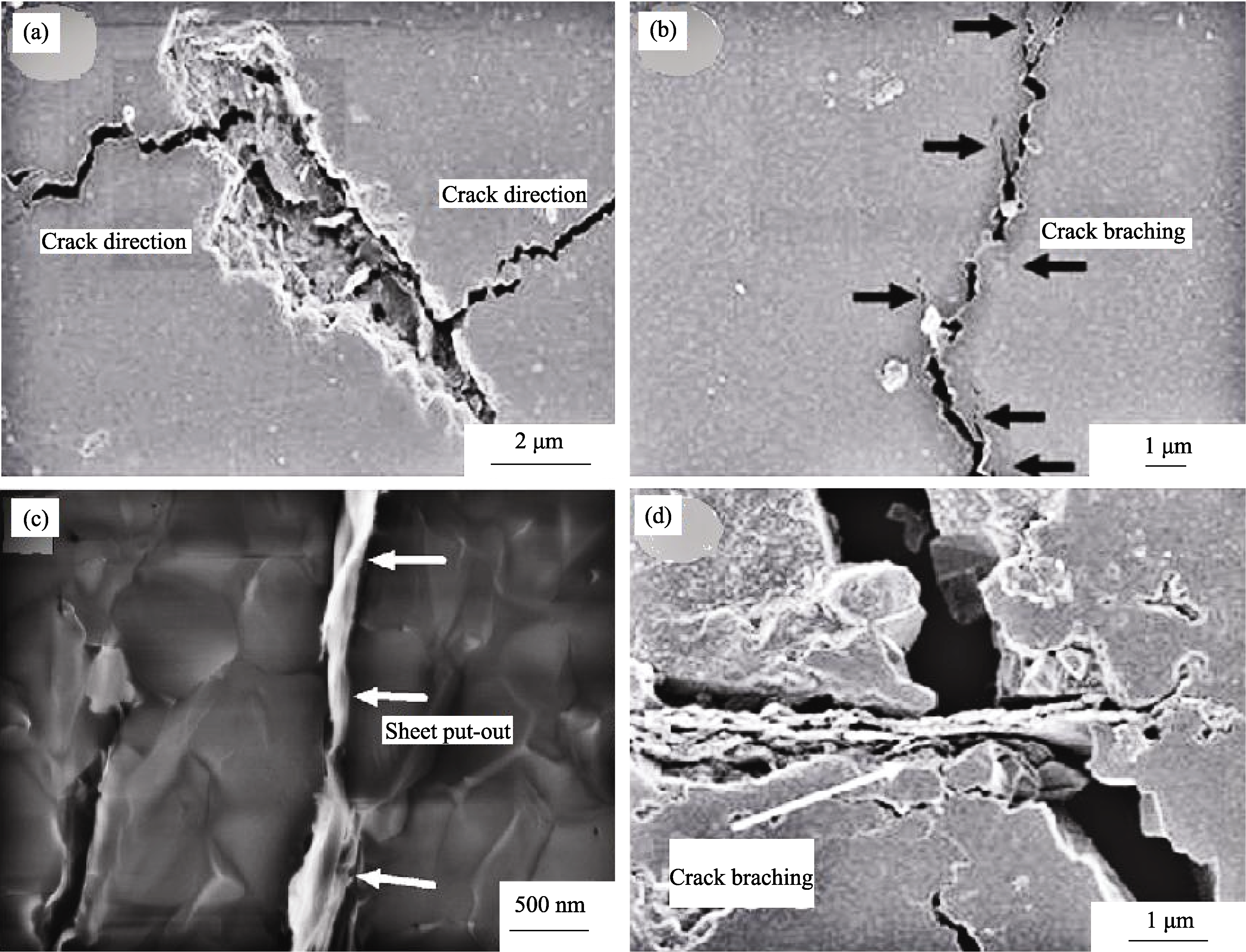
图 10 复合材料的增韧机制
Fig. 10 Toughening mechanisms of composites (a) Crack deflection on a plane with larger size and crack plane orientation almost parallel (fracture line)[29]; (b) Crack branching during crack propagation in the nanographene platelet-reinforced composite (fracture line)[34]; (c) Sheet put-out with a GPL on the fracture surface, with the plane of the sheet perpendicular to the plane of the fracture surface[28]; (d) Crack bridging by GPLs on the fracture line with the plane orientated of sheet nearly perpendicular to the plane of the polished surface[34]
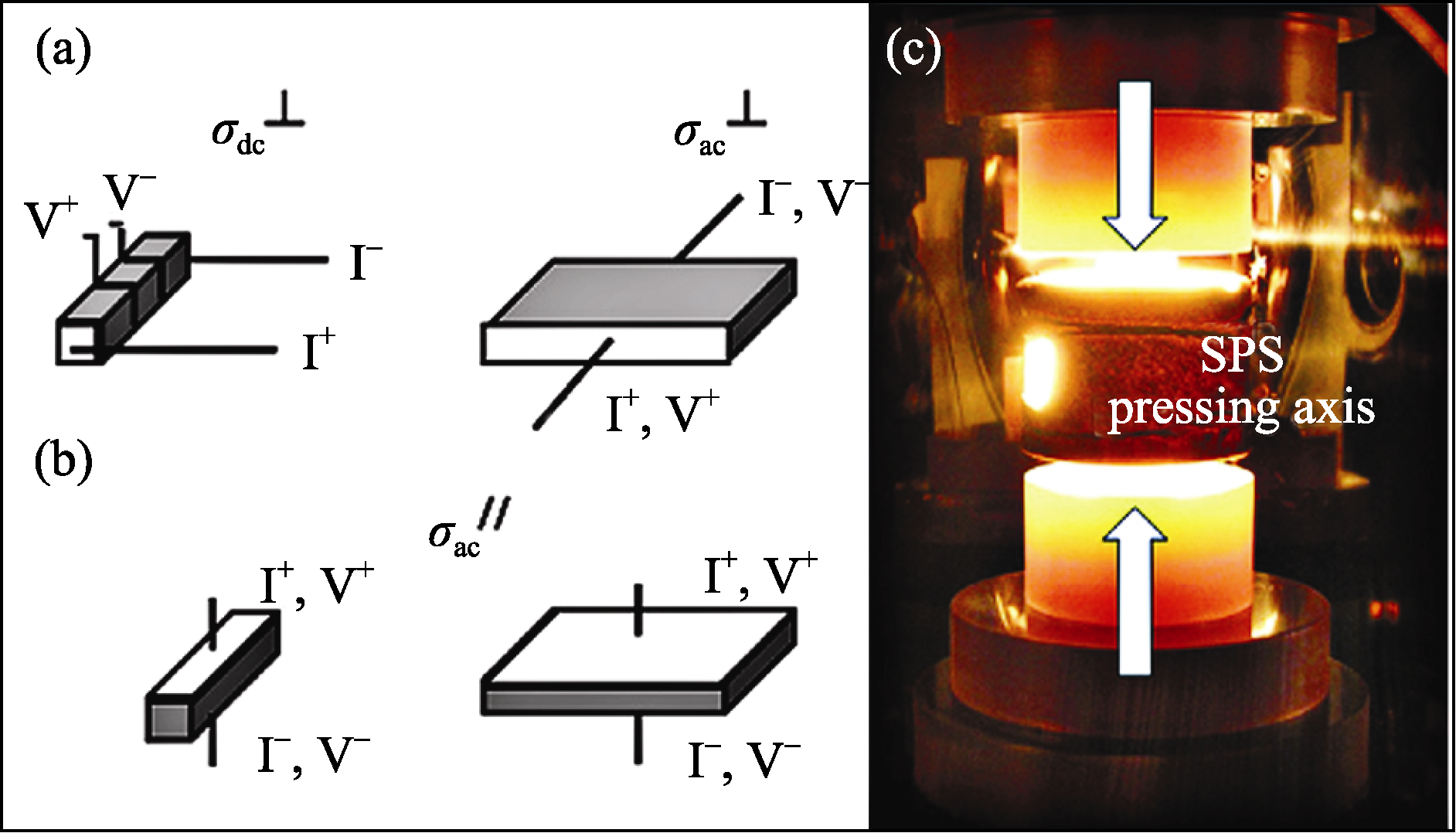
图11 沿着2个方向测量直流和交流电导率的实验装置示意图
Fig. 11 Diagram of experimental setup of dc and ac electrical conductivity (σdc ,σac) measurements along different directions[35] (a) perpendicular (defined by superscript┴) and (b) parallel (superscript″) to the SPS pressing axis; (c) sample and graphite die in the SPS furnace
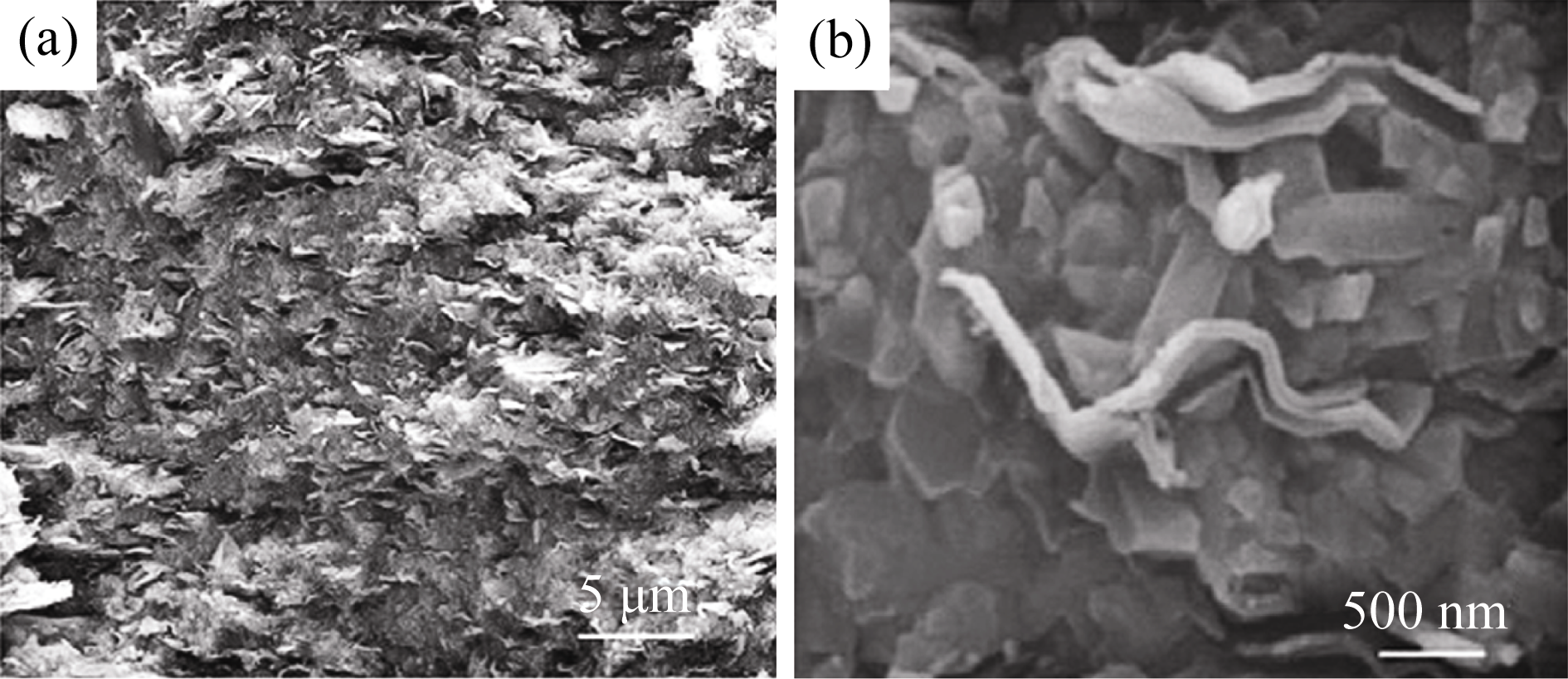
图12 Si3N4/GNP块体复合材料的断面FESEM照片(a)和高倍率图像显示纳米片沿着基体晶界Z字形弯曲(b)[36]
Fig. 12 FESEM micrographs of the fracture surface of the Si3N4/GNP composite where nanoplatelets protrude from the surface (a) and high magnification image showing the zigzag bending of nanoplatelets along the matrix grain boundaries (b)[36]
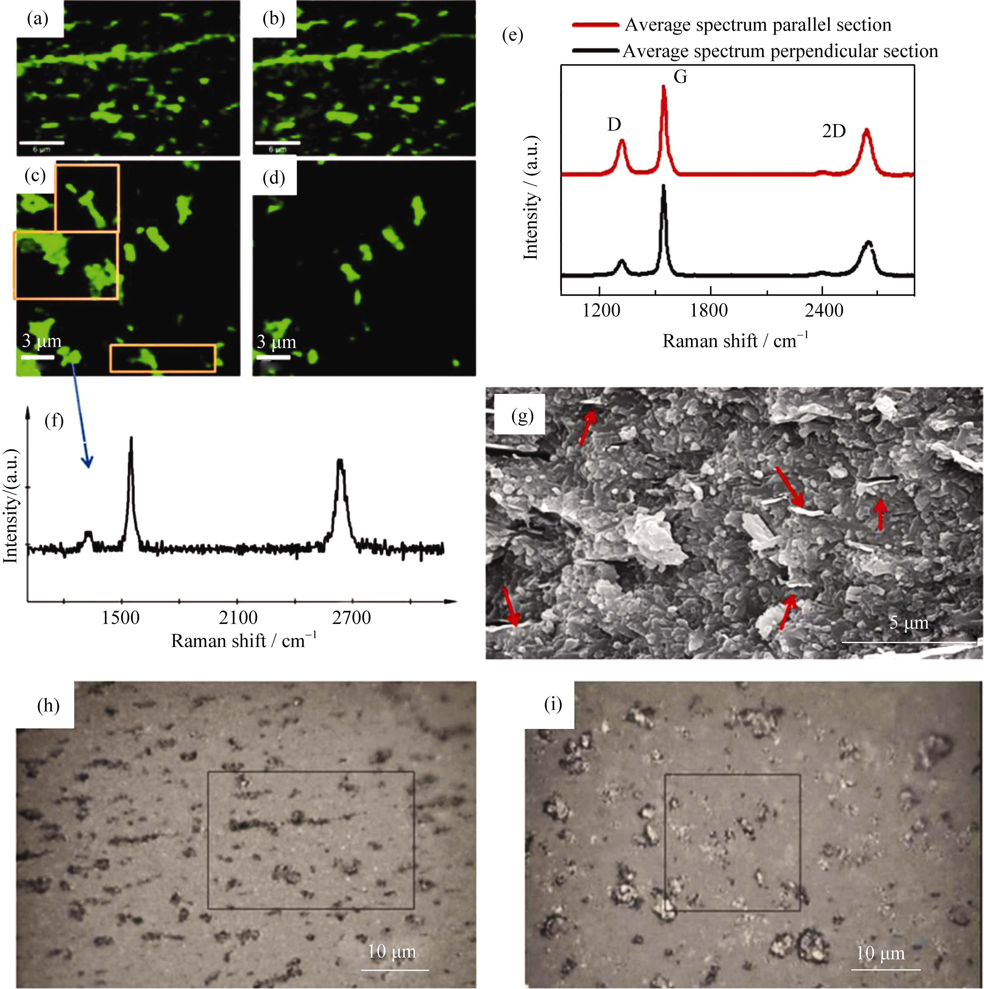
图13 对于复合材料的两个取向: 平行(a和b)和垂直(c和d)于SPS压轴线, 由G(a和c)和D(b和d)峰强度建立的拉曼图像; (e)为两个扫描区域的平均光谱图; (f)为具有2D峰强度的多层石墨烯单一频谱图, 该单一频谱是从集合的(c)图中提取的; (g)为断面(平行取向)SEM照片, 显示了GNPs的(箭头所指)择优取向; (h和i)为平行(左)和垂直(右)于SPS压轴的两个样品取向的扫描区域(轮廓)的光学图像[38]
Fig. 13 Raman images built from G (a and c) and D peak intensities (b and d) for both composite orientations: parallel (a and b) and perpendicular (c and d) to the SPS pressing axis. Average spectra of both scanned regions (e). Example of a single spectrum extracted from the collection of image (c) with the intense 2D peak of few layer graphene (f). SEM micrograph of the fracture surface (parallel orientation) (g), showing the preferential orientation of projected GNPs (pointed by arrows). (h and i) Optical images of the scanned zones (outlined) for both specimen orientations parallel (left) and perpendicular (right) to the SPS axis[38]
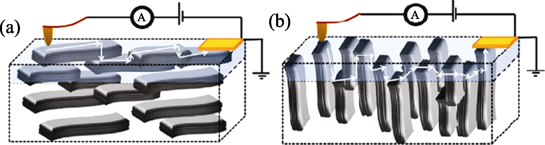
图14 几何形状测量电流的简化原理图(在样品表面边缘的对电极), (a)垂直于SPS加压轴线的导电路径; (b)平行于SPS加压轴线的导电路径[36]
Fig. 14 Simplified schematics of the measuring geometry (counter-electrode at the sample surface edge) to illustrate the conducting paths for the orientations perpendicular (a) and parallel (b) respect to the SPS pressing axis[36]
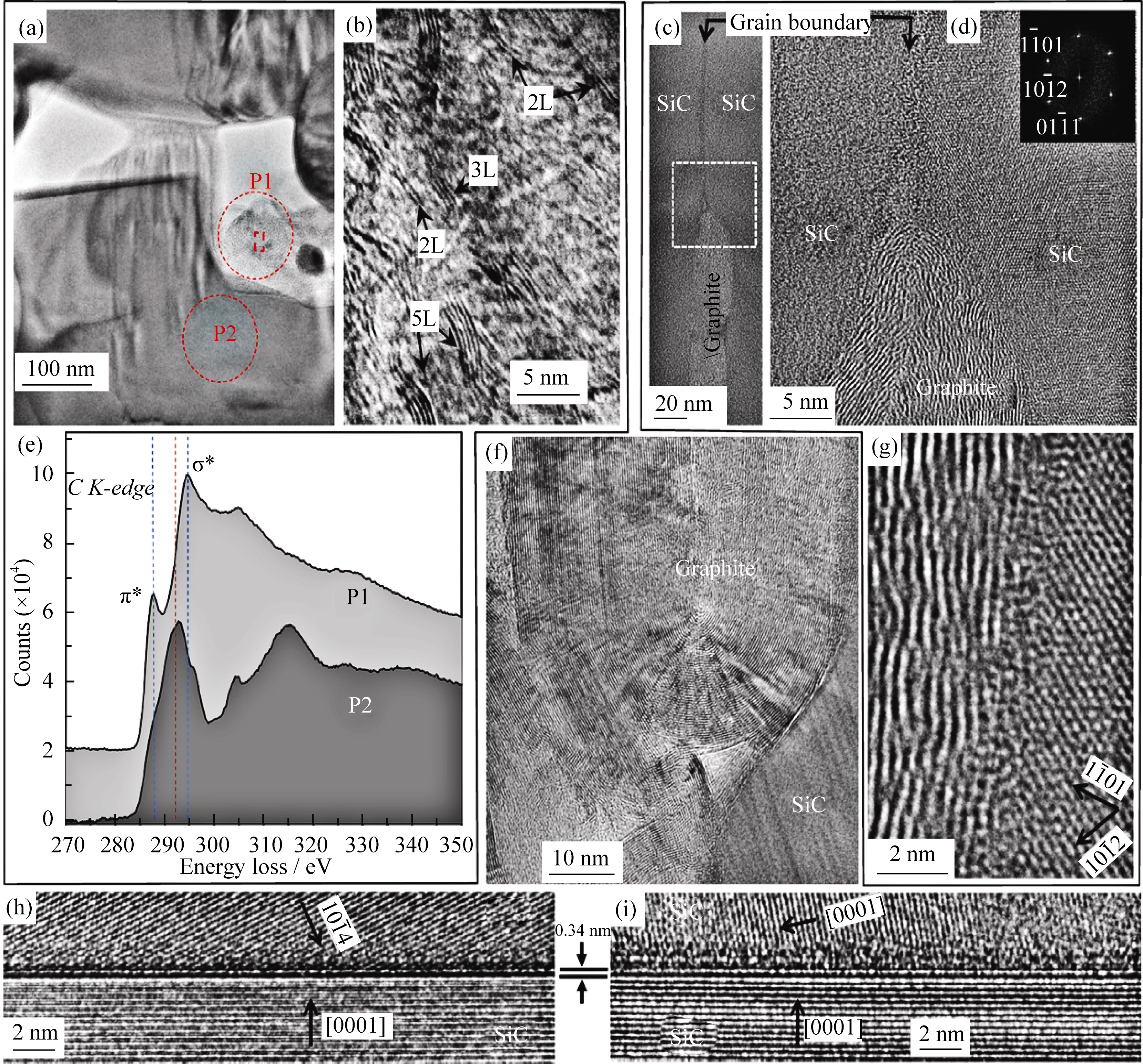
图15 α-SiC复合材料样品的TEM照片, 显示了不同石墨烯层数的几个区域。1区: (a)研究区域的低倍率TEM照片, (b)是富含SP2杂化区的P1区域(突出显示的矩形区域)的高倍率图像, 显示了少层石墨烯片(2L、3L和5L)的不同截面; 暗线条线之间的间距与石墨烯之间一致。(e)是分别在P1和P2位置碳K边界的电子能量损失谱(去除多重散射背景后)。2区: (c)具有形成石墨岛屿晶界的低倍率TEM照片, (d,g)是同一区域的高分辨率TEM照片, 插图是右侧SiC颗粒的电子衍射图。3区:(f)几十纳米的石墨形成区。4区: (h和i)代表双层石墨烯的两个不同晶界[40]
Fig. 15 TEM images of the α-SiC composite sample, showing several regions with different number of graphene layers. Region 1: (a) low magnification TEM image of the region of interest. (b) is a higher magnification image of the P1 region (inside the highlighted rectangular region) which is rich in sp2 carbon, showing different cross-section views of few-layers graphene flakes (2L, 3L and 5L); the spacing between dark contrast lines is consistent with the spacing between graphene sheets. (e) are electron energy loss spectroscopy spectra (after multiple-scattering background removal) of the carbon K edge at positions P1 and P2, respectively. Region 2: (c) low magnification TEM image of a grain boundary with formation of a graphite island, (d, g) high-resolution TEM images of the same region, the inset is SEAD of the right side SiC grain. Region 3: (f) graphitic formation of several tens of nanometers. Region 4: (h and i) two different grain boundaries presenting bi-layer graphene[40]
| [1] | GEIM A K, NOVOSELOV K S. The rize of graphene. Nature Materials, 2007, 6(3): 183-191. |
| [2] | NOVOSELOV K S, GEIM A K, MOROZOV S V, et al. Electric field effect in atomically thin carbon films. Science, 2004, 306(5696): 666-669. |
| [3] | WEITZ R T, YACOBY A. Nanomaterials: graphene rests easy. Nat. Nanotechnol., 2010, 5(10): 699-700. |
| [4] | LEE C, WEI X, KYSAR J W, et al. Measurement of the elastic properties and intrinsic strength of monolayer grapheme. Science, 2008, 321(5887): 385-388. |
| [5] | GEIM A K. Graphene: status and prospects. Science, 2009, 324(5934): 1530-1534. |
| [6] | VAN B J. Graphene: from strength to strength. Nat. Nanotechnol., 2007, 2(4): 199-201. |
| [7] | NAIR R, BLAKE P, GRIGORENKO A, et al. Fine structure constant defines visual transparency of grapheme. Science, 2008, 320(5881): 1308. |
| [8] | NOVOSELOV K S, JIANG Z, ZHANG Y, et al. Room-temperature quantum hall effect in grapheme. Science, 2007, 315(5817): 1379. |
| [9] | KATSNELSON M I, NOVOSELOV K S, GEIM A K. Chiral tunnelling and the Klein paradox in graphene. Nat. Phys., 2006, 2(9): 620-625. |
| [10] | HEERSCHE H B, JARILLO-HERRERO P, OOSTINGA J B, et al. Bipolar supercurrent in graphene. Nature, 2007, 446(7131): 56-59. |
| [11] | WANG Y, HUANG Y, SONG Y, et al. Room temperature ferromagnetism of grapheme. Nano Lett., 2009, 9(1): 220-224. |
| [12] | ZHAO Y, HUANG W J. Research progress on preparation and performance of grephene and its composite. Journal of Chongqing University of Technology (Natural Science), 2011, 7(25): 64-70. |
| [13] | XIE P, LU Q, WANG L E, et al. Research progress in preparation and modify of graphene and polymers/graphene nanocomposities. Materials Review, 2010, 11(24): 163-166. |
| [14] | LI Y X, CHEN Y, ZHUANG X D, et al. Chemistry and potential application of graphene. Journal of Shanghai Second Polytechnic University, 2010, 4(27): 259-269. |
| [15] | LI J L, BAI G Z, WANG L J, et al. Microstructure and mechanical properties of in-situ produced TiC/C nanocomposite. Scripta Materialia, 2005, 52(9): 867-871. |
| [16] | LI J L, BAI G Z, WANG L J, et al. Microstructure and mechanical properties of hot-pressed bulk carbon nanotubes compacted by spark plasma sintering. Carbon, 2005, 43(13): 2649-2653. |
| [17] | LI J L, WANG L J, JIANG W, et al. Surface graphitization and mechanical properties of hot-pressed bulk carbon nanotubes compacted by spark plasma sintering. Carbon, 2007, 45(13): 2636-2642. |
| [18] | CHEN J T, CHEN L Q, ZHANG Z C, et al. Graphene layers produced from carbon nanotubes by friction. Carbon, 2012, 50(5): 1934-1941. |
| [19] | JI F, LI Y L, FENG J M, et al. Electrochemical performance of graphene nanosheets and ceramic composites as anodes for lithium batteries. J. Mater. Chem., 2009, 19(47): 9603-9607. |
| [20] | KANG Y R, JI F, LI Y L, et al. Synthesis of graphite oxides by chemical oxidation method and ceramic composites. Journal of the Chinese Ceramic Society, 2010, 8(38): 1558-1561. |
| [21] | HE T, LI J L, WANG L J, et al. Preparation and consolidation of alumina/graphene composite powders. Materials Transactions, 2009, 50(4): 749-751. |
| [22] | FAN Y C, WANG L J, LI J L, et al. Preparation and electrical properties of graphene nanosheet/Al2O3 composites. Carbon, 2010, 48(6): 1743-1749. |
| [23] | FAN Y C, JIANG W, AKIRA K. Highly conductive few-layer graphene/Al2O3 nanocomposites with tunable charge carrier type. Advanced Functional Materials, 2012, 22(18): 3882-3889. |
| [24] | WANG K, WANG Y F, WEI T, et al. Preparation of graphene nanosheet/alumina composites by spark plasma sintering. Materials Research Bulletin, 2011, 46(2): 315-318. |
| [25] | LIU J, YAN H X, MIKE J R, et al. Toughening of zirconia/alumine composites by the addition of graphene plateles. Journal of the Europen Ceramic Society, 2012, 32(16): 4185-4193. |
| [26] | LIU J, YAN H X, JIANG K. Mechanical properties of graphene platelet-reinforced alumina ceramic composites. Ceramics International, 2013, 39(6): 6215-6221. |
| [27] | WALKER L S, MAROTTO V R, RAFIEE M A, et al. Toughening in graphene ceramic composites. ACS Nano, 2011, 4(5): 3182-3190. |
| [28] | KUN P, TAPASZTÓ O, WÉBER F, et al. Determination of structural and mechanical properties of multilayer graphene added silicon nitride-based composites. Ceramics International, 2012, 38(1): 211-216. |
| [29] | DUSZA J, MORGIEL J, DUSZOVÁ A, et al. Microstructure and fracture toughness of Si3N4+ graphene platelet composites. Journal of the European Ceramic Society, 2012, 32(12): 3389-3397. |
| [30] | KVETKOVÁ L, DUSZOVÁ A, KAŠIAROVÁ M, et al. Influence of processing on fracture toughness of Si3N4 + graphene platelet composites. Journal of the European Ceramic Society, 2013, 33(12): 2299-2304. |
| [31] | TAPASZTÓ O, TAPASZTÓ L, MARKÒ M, et al. Dispersion patterns of graphene and carbon nanotubes in ceramic matrix composites. Chemical Physics Letters, 2011, 511(4/5/6): 340-343. |
| [32] | BELMONTE M, RAM-REZ C, JULIAN J G, et al. The beneficial effect of graphene nanofillers on the tribological performance of ceramics. Carbon, 2013, 61: 431-435. |
| [33] | HVIZDOŠ P, DUSZA J, BALÁZSI C. Tribological properties of Si3N4- graphene nanocomposites. Journal of the European Ceramic Society, 2013, 33(12): 2359-2364. |
| [34] | KVERTKOVÁ L, DUSZOVÁ A, HVIZDOŠ P, et al. Fracture toughness and toughening mechanisms in graphene platelet reinforced Si3N4 composites. Scripta Materialia, 2012, 66(10): 793-796. |
| [35] | RAMIREZ C, FIGUEIREDO F M, MIRANZO P, et al. Graphene nanoplatelet/silicon nitride composites with high electrical conductivity. Carbon, 2012, 50(10): 3607-3615. |
| [36] | RAMIREZ C, GARZÓN L, MIRANZO P, et al. Electrical conductivity maps in graphene nanoplatelet/silicon nitride composites using conducting scanning force microscopy. Carbon, 2011, 49(12): 3873-3880. |
| [37] | RAMÍRZE C, VEGA-DIAZ S M, FIGUEIREDO F M, et al. Synthesis of conducting graphene/Si3N4 composites by spark plasma sintering. Carbon, 3013, 57: 425-432. |
| [38] | RAMIREZ C, OSENDI M I. Characterzation of graphene nanoplateles-Si3N4 composites by Raman spectroscopy. Journal of the European Ceramic Society, 2013, 33(3): 471-477. |
| [39] | MIRANZO P, GARCÍA E, RAMÍREZ C, et al. Anisotropic thermal conductivity of silicon nitride ceramics containing carbon nanostructures. Journal of the European Ceramic Society, 2012, 32(8): 1847-1854. |
| [40] | MIRANZO P, GARCÍA E, RAMÍREZ C, et al. In situ processing of electrically conducting graphene/SiC nanocomposites. Journal of the European Ceramic Society, 2013, 33(10): 1665-1674. |
| [41] | YADHUKULAKRISHNAN G B, KARUMURI S, RAHMAN A, et al. Spark plasma sintering of graphene reinforced zirconium diboride ultra- high temperature ceramic composites. Ceramics International, 2013, 39(6): 6637-6649. |
| [1] | 陈明俊, 缪洪康, 肖英俊, 邓建波, 张翔, 赵九蓬, 李垚. 光-热双响应材料研究进展: 从设计策略到智能窗应用[J]. 无机材料学报, 2026, 41(6): 723-738. |
| [2] | 王萌萌, 田力, 张俊敏, 李庆刚, 杨金山, 董绍明. 3D打印制备CNT/SiC-SiO2及其电磁屏蔽性能[J]. 无机材料学报, 2026, 41(6): 831-838. |
| [3] | 宋坤洁, 解荣军. 机器学习驱动新型发光材料的研究进展[J]. 无机材料学报, 2026, 41(6): 689-703. |
| [4] | 胡钰晴, 朱一新, 乐先浩, 万青. 钽酸锂晶圆减薄技术及其热释电红外探测器应用进展[J]. 无机材料学报, 2026, 41(6): 764-774. |
| [5] | 刘春帆, 陈科, 葛芳芳, 黄庆. 核用耐铅铋腐蚀涂层的研究进展[J]. 无机材料学报, 2026, 41(6): 775-786. |
| [6] | 胡扬, 谢敏, 张筱怡, 李想, 郭新伟, 姜南, 周文瀚, 张胜利, 曾海波. 计算与数据驱动环保型发光材料的研究进展[J]. 无机材料学报, 2026, 41(6): 704-722. |
| [7] | 洪恩柳, 涂欣晨, 李自清, 方晓生. 二维钙钛矿单晶纳米片的漂浮法制备及其光电探测性能[J]. 无机材料学报, 2026, 41(6): 787-794. |
| [8] | 王俊卜, 黄泽皑, 杨茗凯, 蒙颖, 周明炜, 周莹. 甲烷转化用抗积碳催化材料研究进展[J]. 无机材料学报, 2026, 41(6): 739-750. |
| [9] | 王金文, 杨振, 周欢, 夏丹, 杨磊. 可注射无机材料及其生物医学应用[J]. 无机材料学报, 2026, 41(6): 751-763. |
| [10] | 孙丽, 徐永善, 高义华. 石墨烯/Bi2O2Se/石墨烯双异质结器件的光探测和仿生突触研究[J]. 无机材料学报, 2026, 41(6): 795-804. |
| [11] | 汪加辉, 刘晶晶, 邱毅, 王永霞, 崔香枝. 原子级铁锚定氮掺杂石墨烯的双功能氧电催化性能[J]. 无机材料学报, 2026, 41(6): 814-822. |
| [12] | 高科丰, 何昕昕, 刘增乾, 张哲峰. 多尺度类贝壳珍珠质层状与梯度结构仿生陶瓷-树脂复合材料[J]. 无机材料学报, 2026, 41(5): 573-582. |
| [13] | 李涵涛, 沈强, 罗国强, 王雪飞, 高明, 陈晨. 机械球磨法调控硅基负极材料结构与性能的研究进展[J]. 无机材料学报, 2026, 41(5): 561-572. |
| [14] | 解陈一, 缪花明, 张蔚然, 刘荣军, 王衍飞, 李端. 理论计算在高熵陶瓷领域的研究进展[J]. 无机材料学报, 2026, 41(5): 545-560. |
| [15] | 王雅娜, 宋九鹏, 王海润, 李天山, 焦健. MI-SiCf/SiC复合材料开孔拉伸性能孔径效应研究[J]. 无机材料学报, 2026, 41(5): 653-662. |
| 阅读次数 | ||||||
|
全文 |
|
|||||
|
摘要 |
|
|||||