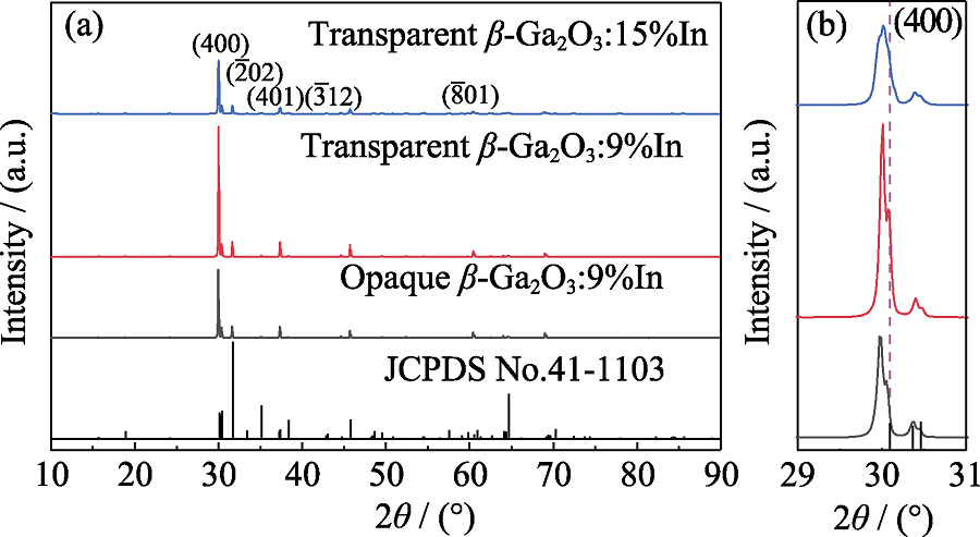
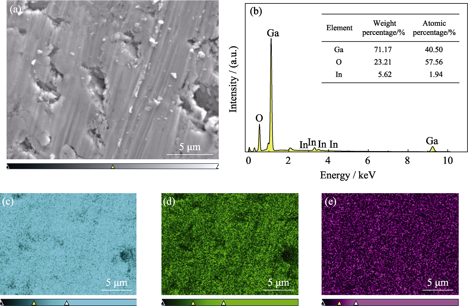
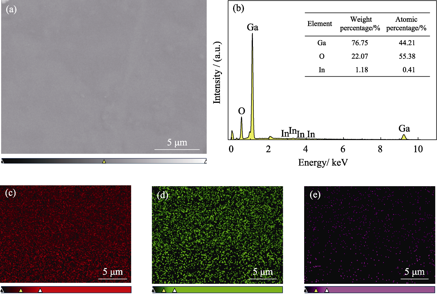
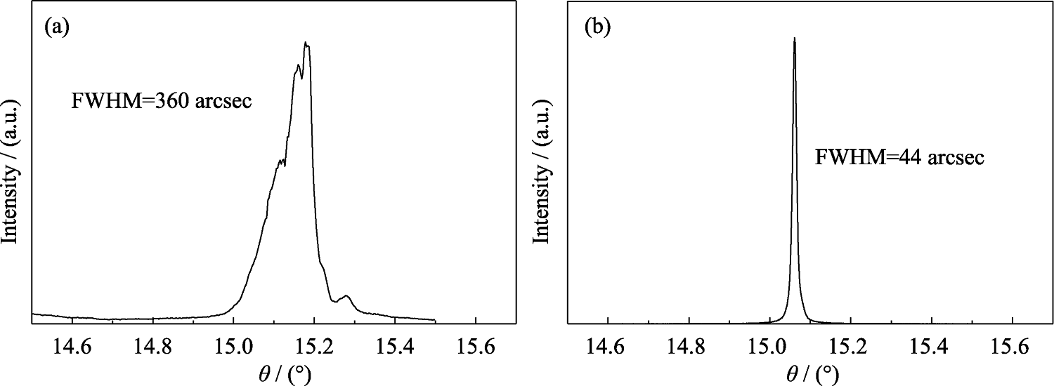
| [1] |
ZHANG J, LI B, XIA C, et al. Growth and spectral characterization of β-Ga2O3 single crystals. Journal of Physics and Chemistry of Solids, 2006, 67(12): 2448.
|
| [2] |
TIPPINS H H. Optical absorption and photoconductivity in the band edge of β-Ga2O3. Physical Review, 1965, 140(1A): A316.
|
| [3] |
MATSUMOTO T, AOKI M, KINOSHITA A, et al. Absorption and reflection of vapor grown single crystal platelets of β-Ga2O3. Japanese Journal of Applied Physics, 1974, 13(10): 1578.
|
| [4] |
RICCI F, BOSCHI F, BARALDI A, et al. Theoretical and experimental investigation of optical absorption anisotropy in β-Ga2O3. Journal of Physics: Condensed Matter, 2016, 28(22): 224005.
|
| [5] |
ONUMA T, SAITO S, SASAKI K, et al. Valence band ordering in β-Ga2O3 studied by polarized transmittance and reflectance spectroscopy. Japanese Journal of Applied Physics, 2015, 54(11): 112601.
|
| [6] |
HE N, TANG H, LIU B, et al. Ultra-fast scintillation properties of β-Ga2O3 single crystals grown by floating zone method. Nuclear Instruments and Methods in Physics Research Section A: Accelerators, Spectrometers, Detectors and Associated Equipment, 2018, 888: 9.
|
| [7] |
GALAZKA Z, GANSCHOW S, SEYIDOV P, et al. Two inch diameter, highly conducting bulk β-Ga2O3 single crystals grown by the Czochralski method. Applied Physics Letters, 2022, 120(15): 152101.
|
| [8] |
UEDA Y, IGARASHI T, KOSHI K, et al. Two-inch Fe-doped β-Ga2O3 (010) substrates prepared using vertical bridgman method. Japanese Journal of Applied Physics, 2023, 62: SF1006.
|
| [9] |
TANG H, HE N, ZHANG H, et al. Inhibition of volatilization and polycrystalline cracking, and the optical properties of β-Ga2O3 grown by the EFG method. CrystEngComm, 2020, 22(5): 924.
|
| [10] |
LI Z, CHEN J, TANG H, et al. Band gap engineering in β-Ga2O3 for a high-performance X-ray detector. ACS Applied Electronic Materials, 2021, 3(10): 4630.
|
| [11] |
ZHANG C, TANG H, LI J, et al. Boltzmann thermometer with broadband emission in Mn4+-doped β-Ga2O3 crystals. Journal of Luminescence, 2024, 267: 120334.
|
| [12] |
XIAO H, SHAO G, SAI Q, et al. Wide Bandgap engineering of β-(Al, Ga)2O3 mixed crystals. Journal of Inorganic Materials, 2016, 31(11): 1258.
|
| [13] |
KPKUBUN Y, ABE T, NAKAGOMI S. Sol-Gel prepared (Ga1-xInx)2O3 thin films for solar-blind ultraviolet photodetectors. Physica Status Solidi (a), 2010, 207(7): 1741.
|
| [14] |
SEACAT S, LYONS J L, PEELAERS H. Properties of orthorhombic Ga2O3 alloyed with In2O3 and Al2O3. Applied Physics Letters, 2021, 119(4): 042104.
|
| [15] |
SHAIK E B, KAMAL C S, SRINIVASU K, et al. Optical insights of indium-doped β-Ga2O3 nanoparticles and its luminescence mechanism. Journal of Materials Science: Materials in Electronics, 2020, 31(8): 6185.
|
| [16] |
LIN T, XIE C, YANG S, et al. Investigation on the bandgap- adjustable (Ga1-xInx)2O3 film prepared by magnetron sputtering. ACS Applied Electronic Materials, 2024, 6(3): 1858.
|
| [17] |
SUN S M, LIU W J, WANG Y P, et al. Band alignment of In2O3/ β-Ga2O3 interface determined by X-ray photoelectron spectroscopy. Applied Physics Letters, 2018, 113(3): 031603.
|
| [18] |
TANG H, WU Q, LUO P, et al. Growth and property of In:Ga2O3 oxide semiconductor single crystal. Journal of Inorganic Materials, 2017, 32(6): 621.
|
| [19] |
GALAZKA Z, UECKER R, IRMSCHER K, et al. Melt growth, characterization and properties of bulk In2O3 single crystals. Journal of Crystal Growth, 2013, 362: 349.
|
| [20] |
OSHIMA T, FUJITA S. Properties of Ga2O3-based (InxGa1-x)2O3 alloy thin films grown by molecular beam epitaxy. Physica Status Solidi (c), 2008, 5(9): 3113.
|
| [21] |
ZHANG F, SAITO K, TANAKA T, et al. Wide bandgap engineering of (GaIn)2O3 films. Solid State Communications, 2014, 186: 28.
|
| [22] |
ZHANG F, SUN J, LI H, et al. Band-gap tunable (GaxIn1-x)2O3 layer grown by magnetron sputtering. Frontiers of Information Technology & Electronic Engineering, 2021, 22(10): 1370.
|
| [23] |
VASYLTSIV V I, RYM Y I, ZAKHARKO Y M. Optical absorption and photoconductivity at the band edge of β-Ga2-xInxO3. Physica Status Solidi (b), 1996, 195(2): 653.
|
| [24] |
WU Q, TANG H, SU L, et al. Growth and properties of β-Ga2O3:In single crystal by optical floating zone method. Journal of the Chinese Ceramic Society, 2017, 45(4): 548.
|
| [25] |
LI Z, TANG H, LI Y, et al. Enhanced scintillation performance of β-Ga2O3 single crystals by Al3+ doping and its physical mechanism. Applied Physics Letters, 2022, 121(10): 102102.
|
| [26] |
TANG H, HE N, ZHU Z, et al. Temperature-dependence of X-ray excited luminescence of β-Ga2O3 single crystals. Applied Physics Letters, 2019, 115(7): 071904.
|
| [27] |
VARLEY J B, WEBER J R, JANOTTI A, et al. Oxygen vacancies and donor impurities in β-Ga2O3. Applied Physics Letters, 2010, 97(14): 142106.
|
| [28] |
WANG V, XIAO W, KANG L J, et al. Sources of n-type conductivity in GaInO3. Journal of Physics D: Applied Physics, 2015, 48(1): 015101.
|
| [29] |
VÍLLORA E G, YAMAGA M, INOUE T, et al. Optical spectroscopy study on β-Ga2O3. Japanese Journal of Applied Physics, 2002, 41: L622.
|
| [30] |
ISLAM M M, RANA D, HERNANDEZ A, et al. Study of trap levels in β-Ga2O3 by thermoluminescence spectroscopy. Journal of Applied Physics, 2019, 125(5): 055701.
|
 ), 张超逸, 黄林, 孙鹏, 刘波, 徐军, 唐慧丽(