无机材料学报 ›› 2023, Vol. 38 ›› Issue (3): 243-255.DOI: 10.15541/jim20220607 CSTR: 32189.14.10.15541/jim20220607
齐占国1( ), 刘磊1, 王守志1(), 王国栋1, 俞娇仙2, 王忠新1, 段秀兰1, 徐现刚1, 张雷1()
收稿日期:2022-10-17
修回日期:2022-11-20
出版日期:2023-03-20
网络出版日期:2023-01-17
通讯作者:
王守志, 研究员. E-mail: wangsz@sdu.edu.cn;作者简介:齐占国(1999-), 男, 博士研究生. E-mail: zhan_guo_2021@163.com
基金资助:
QI Zhanguo1(), LIU Lei1, WANG Shouzhi1(), WANG Guogong1, YU Jiaoxian2, WANG Zhongxin1, DUAN Xiulan1, XU Xiangang1, ZHANG Lei1()
Received:2022-10-17
Revised:2022-11-20
Published:2023-03-20
Online:2023-01-17
Contact:
WANG Shouzhi, professor. E-mail: wangsz@sdu.edu.cn;About author:QI Zhanguo (1999-), male, PhD candidate. E-mail: zhan_guo_2021@163.com
Supported by:摘要:
相比于第一代和第二代半导体材料, 第三代半导体材料具有更高的击穿场强、电子饱和速率、热导率以及更宽的带隙, 更适用于制备高频、大功率、抗辐射、耐腐蚀的电子器件、光电子器件和发光器件。氮化镓(GaN)作为第三代半导体材料的代表之一, 是制作蓝绿激光、射频微波器件和电力电子器件的理想衬底材料, 在激光显示、5G通信、相控阵雷达、航空航天等领域具有广阔的应用前景。氢化物气相外延(Hydride vapor phase epitaxy, HVPE)方法因生长设备简单、生长条件温和和生长速度快而成为制备GaN晶体的主流方法。由于普遍使用石英反应器, HVPE法生长获得的非故意掺杂GaN不可避免地存在施主型杂质Si和O, 使其表现出n型半导体特性, 但载流子浓度高和导电率低限制了其在高频大功率器件中的应用。掺杂是改善半导体材料电学性能最普遍的方法, 通过掺杂不同掺杂剂可以获得不同类型的GaN单晶衬底, 提高其电化学特性, 从而满足市场应用的不同需求。本文介绍了GaN半导体晶体材料的基本结构和性质, 综述了近年来采用HVPE法生长高质量GaN晶体的主要研究进展; 对GaN的掺杂特性、掺杂剂类型、生长工艺以及掺杂原子对电学性能的影响进行了详细介绍。最后简述了HVPE法生长掺杂GaN单晶面临的挑战和机遇, 并展望了GaN单晶的未来发展前景。
中图分类号:
齐占国, 刘磊, 王守志, 王国栋, 俞娇仙, 王忠新, 段秀兰, 徐现刚, 张雷. GaN单晶的HVPE生长与掺杂进展[J]. 无机材料学报, 2023, 38(3): 243-255.
QI Zhanguo, LIU Lei, WANG Shouzhi, WANG Guogong, YU Jiaoxian, WANG Zhongxin, DUAN Xiulan, XU Xiangang, ZHANG Lei. Progress in GaN Single Crystals: HVPE Growth and Doping[J]. Journal of Inorganic Materials, 2023, 38(3): 243-255.
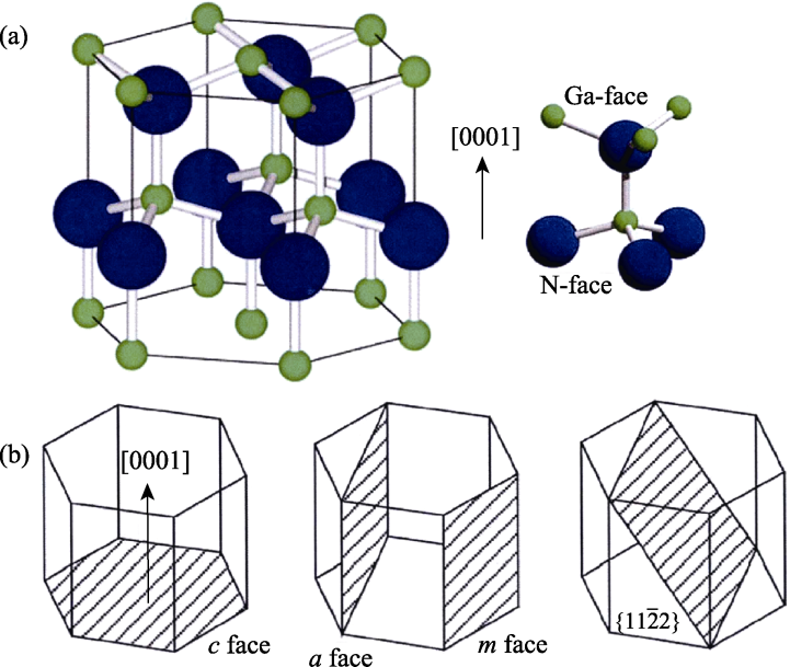
图1 GaN示意图[4]
Fig. 1 Schematic diagram of GaN[4] (a) Hexagonal unit call (left) and the bond structure of GaN (right), with green balls indicating Ga atoms and blue balls indicating N atoms; (b) Polar face (left), non-polar face (middle) and one kind of semi-polar faces (right) of GaN crystal
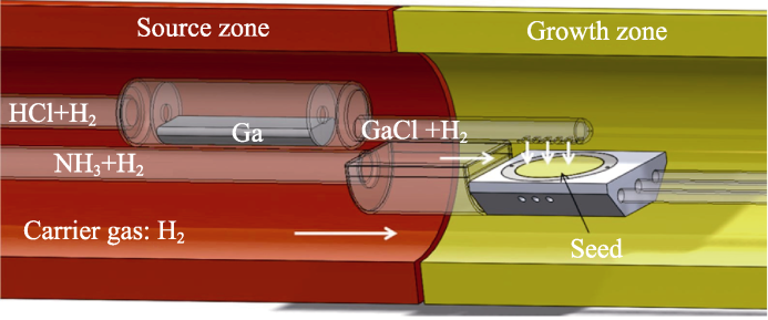
图2 HVPE反应器的结构[8]
Fig. 2 Structure of HVPE reactor[8]
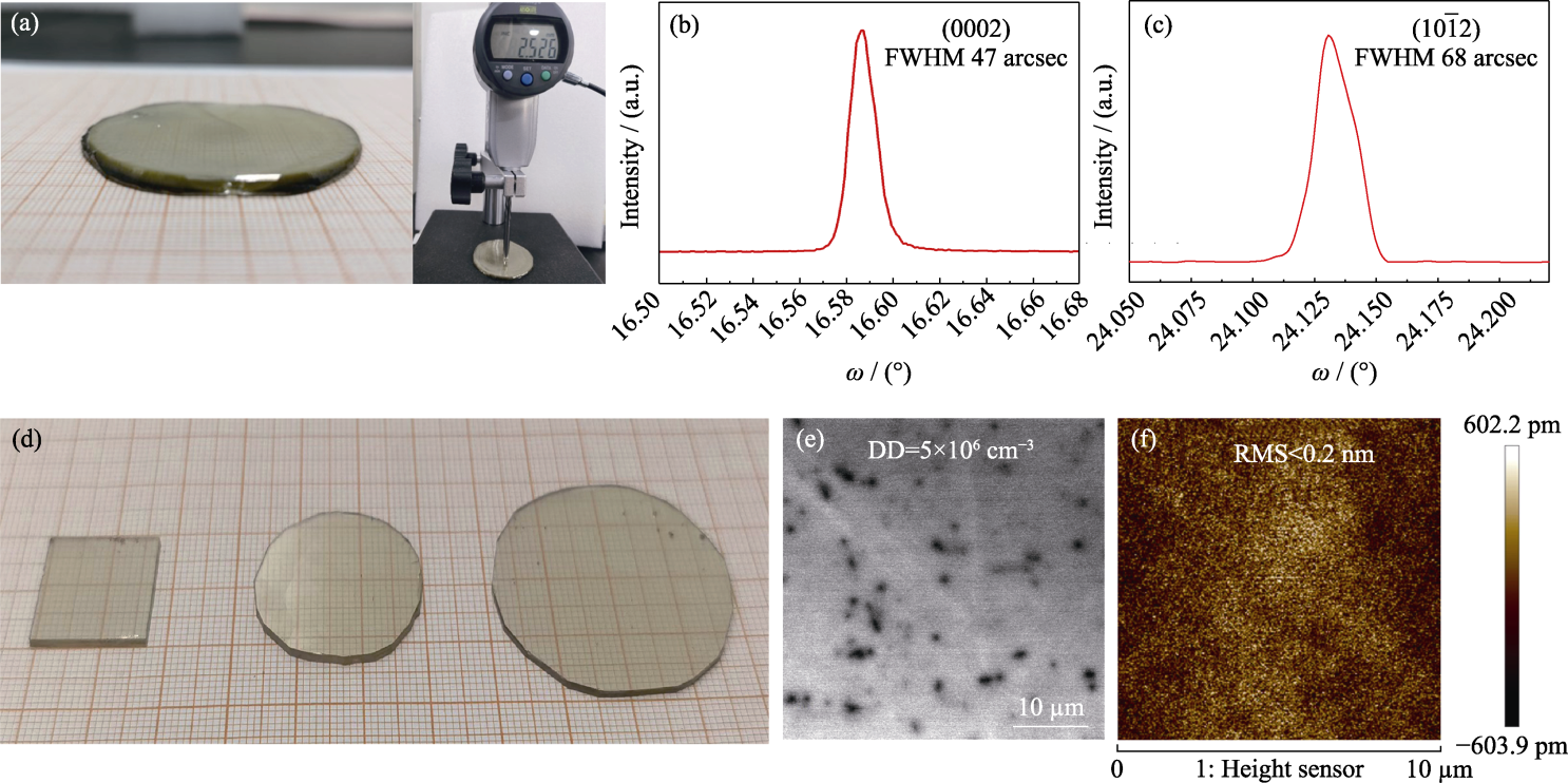
图3 HVPE生长的GaN晶体照片及质量表征
Fig. 3 Photos and characterization of GaN crystals grown by HVPE (a) 2-inch 2.5 mm thick GaN crystal; (b) (0002) surface high-resolution XRD pattern; (c) (10¯12) high-resolution XRD pattern; (d) Image of GaN wafers; (e) CL image (dislocation density ~5×106 cm-2); (f) AFM image (RMS<0.2 nm in the range of 10 μm×10 μm)
| Type | Impurities | Dopant | Characteristic | Application | Ref. |
|---|---|---|---|---|---|
| n type | Si | SiCl2H2 | High carrier concentration; anti-surfactant effect | High power and high current optoelectronic devices (LED, LD) | |
| Ge | GeCl4/Ge3N4 | Little effect on lattice structure and stress, causing no morphological deterioration, higher carriers concentration than that of Si-doped; creating cavities inside the sample | [ | ||
| p type | Mg | Mg(S) | Increased lattice constant and band gap width, high conductivity | Luminescent device | [ |
| Semi- insulating | Fe | Fe(S)/Cp2Fe | High resistivity (iron showing a parasitic effect, easy to diffuse) | High power/frequency devices, HEMT, photoconductive switch, detectors | [ |
| Mn | Mn(S) | ||||
| C | CH4/C2H4/C5H12 |
表1 不同类型掺杂GaN的对比[2-3,32]
Table 1 Different types of doped GaN[2-3,32]
| Type | Impurities | Dopant | Characteristic | Application | Ref. |
|---|---|---|---|---|---|
| n type | Si | SiCl2H2 | High carrier concentration; anti-surfactant effect | High power and high current optoelectronic devices (LED, LD) | |
| Ge | GeCl4/Ge3N4 | Little effect on lattice structure and stress, causing no morphological deterioration, higher carriers concentration than that of Si-doped; creating cavities inside the sample | [ | ||
| p type | Mg | Mg(S) | Increased lattice constant and band gap width, high conductivity | Luminescent device | [ |
| Semi- insulating | Fe | Fe(S)/Cp2Fe | High resistivity (iron showing a parasitic effect, easy to diffuse) | High power/frequency devices, HEMT, photoconductive switch, detectors | [ |
| Mn | Mn(S) | ||||
| C | CH4/C2H4/C5H12 |
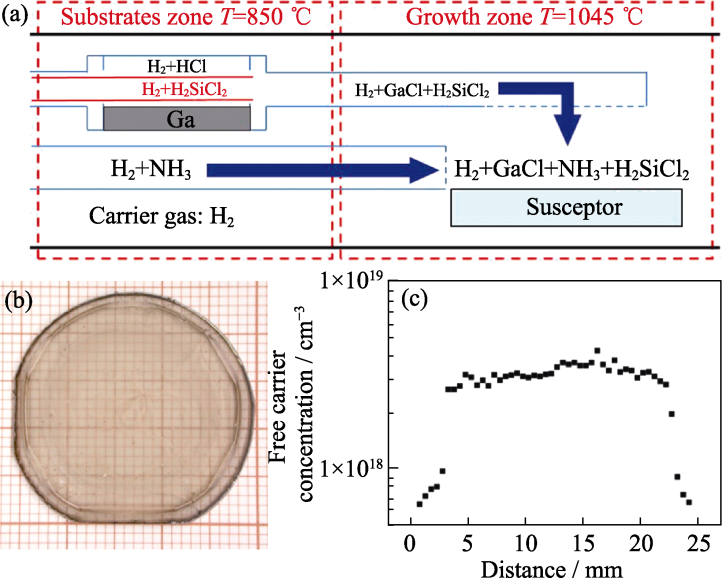
图4 Si掺杂HVPE-GaN[38]
Fig. 4 Si-doped HVPE-GaN[38] (a) Structure of Si-doped HVPE-GaN reactor; (b) Image of 800 μm- thick Si-doped HVPE-GaN; (c) Distribution of free carrier concentration along the diameter of Si-doped HVPE-GaN
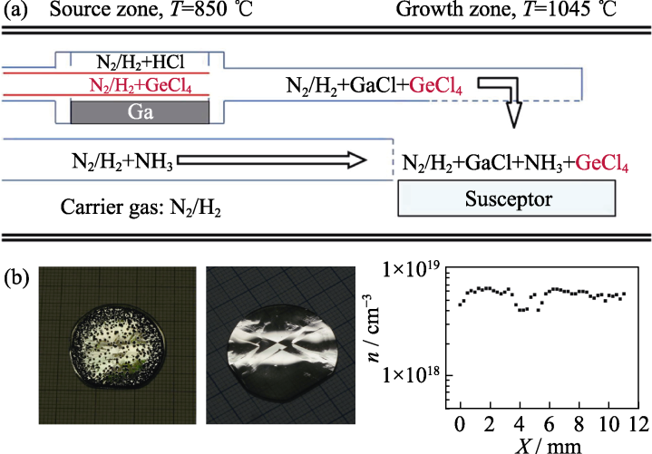
图5 Ge掺杂HVPE-GaN[47]
Fig. 5 Ge-doped HVPE-GaN[47] (a) Structure of Ge-doped HVPE-GaN reactor; (b) Morphologies of Ge-doped HVPE-GaN: crystallized in H2 carrier gas (left), crystallized in N2 carrier gas (middle), distribution of free carrier concentration along the diameter of Ge-doped HVPE-GaN
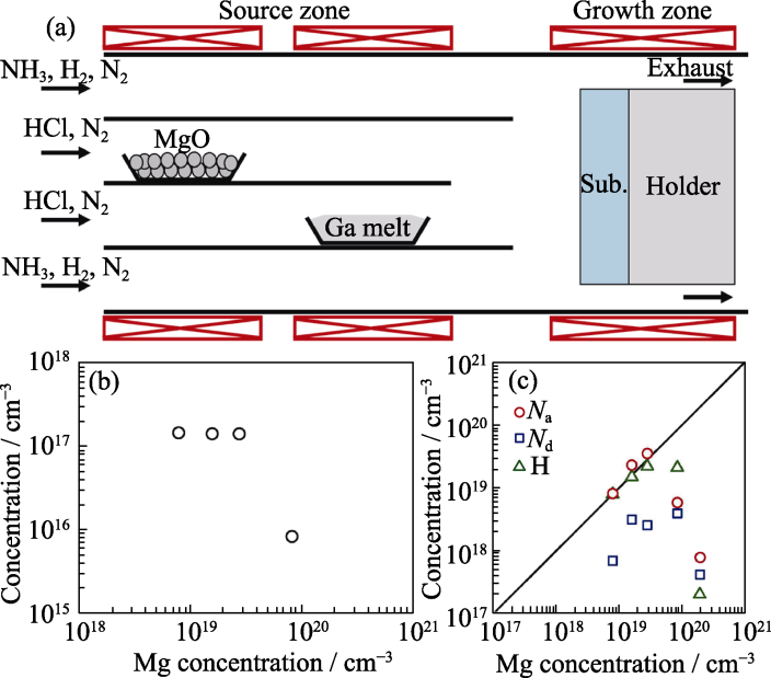
图6 Mg掺杂HVPE-GaN
Fig. 6 Mg-doped HVPE-Ga (a) Schematic of the HVPE system for growth of Mg doped GaN using MgO[53]; (b) Hole concentration measured at room temperature as a function of Mg concentration[55]; (c) Compensating donor concentration (Nd) and acceptor concentration (Na) as a function of Mg concentration[55]
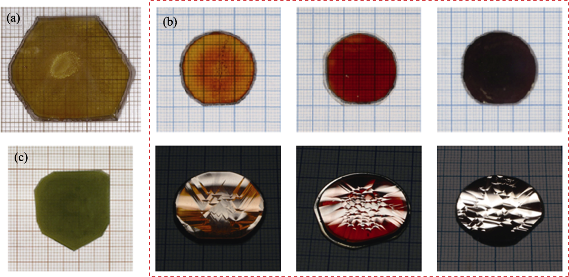
图7 半绝缘GaN晶片形貌图
Fig. 7 Image of semi-insulated GaN wafers (a) Fe-doped[62]; (c) Mn-doped[63]; (b) C-doped[60]
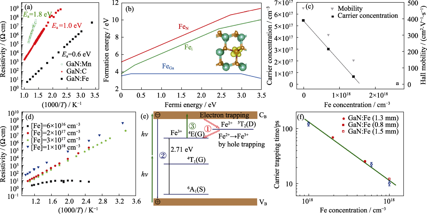
图8 Fe掺杂GaN
Fig. 8 Fe-doped GaN (a) Resistivity as a function of reciprocal temperature for samples doped with Mn, C, and Fe[8]; (b) Formation energy versus Fermi level for FeGa, FeN and Fei in GaN in different charge states, under Ga-rich conditions[68]; (c) Carrier concentration and Hall mobility versus Fe concentration in GaN films co-doped with Si and Fe[70]; (d) Resistivity versus inverse temperature for samples doped with Fe at various Fe concentrations[63]; (e) Schematic diagram of the energy levels and carrier decay processes of Fe-doped GaN[71]; (f) Carrier trapping time for Fe-doped GaN bulk crystals[72]
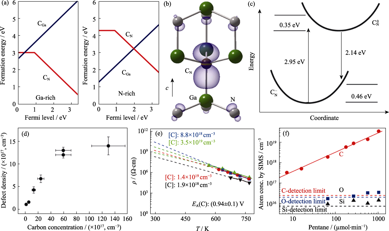
图9 C掺杂GaN
Fig. 9 C-doped GaN (a) Formation energy versus Fermi level for CGa and CN in GaN: Ga-rich conditions (left), and N-rich conditions (right)[79]; (b) CN impurity model in GaN[79]; (c) Optical transitions of CN in GaN[79]; (d) Defect density as a function of C concentration[81]; (e) Temperature-dependent resistivity for C doped GaN[82] ; (f) Concentrations of carbon, oxygen, and silicon in C-doped GaN layers versus the input mole fraction of pentane[82]
| [1] |
HARIMA H. Properties of GaN and related compounds studied by means of Raman scattering. Journal of Physics: Condensed Matter, 2002, 14(38): R967.
DOI URL |
| [2] | ZHANG Y M, WANG J F, CAI D M, et al. Progress on GaN single crystal substrate grown by hydride vapor phase epitaxy. Journal of Synthetic Crystals, 2020, 49(11): 1970. |
| [3] |
ZHANG Y M, WANG J F, CAI D M, et al. Growth and doping of bulk GaN by hydride vapor phase epitaxy. Chinese Physics B, 2020, 29(2): 026104.
DOI |
| [4] | 田媛. HVPE生长自支撑GaN单晶及其性质研究. 济南: 山东大学晶体材料研究所博士学位论文, 2016. |
| [5] | 胡海啸. 自支撑GaN单晶的HVPE生长及加工研究. 济南: 山东大学晶体材料研究所博士学位论文, 2020. |
| [6] |
HSU P S, KELCHNER K M, TYAGI A, et al. InGaN/GaN blue laser diode grown on semipolar (30¯31) free-standing GaN substrates. Applied Physics Express, 2010, 3(5): 052702.
DOI URL |
| [7] |
ABBAS A S, ALYAMANI A Y, NAKAMURA S, et al. Enhancement of n-type GaN (20¯21) semipolar surface morphology in photo-electrochemical undercut etching. Applied Physics Express, 2019, 12(3): 036503.
DOI URL |
| [8] |
BOCKOWSKI M, IWINSKA M, AMILUSIK B, et al. Doping in bulk HVPE-GaN grown on native seeds-highly conductive and semi-insulating crystals. Journal of Crystal Growth, 2018, 499: 1.
DOI URL |
| [9] | VORONENKOV V V, BOCHKAREVA N I, GORBUNOV R I, et al. Two modes of HVPE growth of GaN and related macrodefects. Physica Status Solidi C, 2013, 10(3): 468471. |
| [10] |
LEE M, PARK S. Stress-engineered growth of homoepitaxial GaN crystals using hydride vapor phase epitaxy. RSC Advances, 2018, 8(62): 35571.
DOI URL |
| [11] |
ZHANG L, SHAO Y, HAO X, et al. Improvement of crystal quality HVPE grown GaN on an H3PO4 etched template. CrystEngComm, 2011, 13(15): 5001.
DOI URL |
| [12] | VORONENKOV V V, LELIKOV Y S, ZUBRILOV A S, et al. Thick GaN film stress-induced self-separation. IEEE Conference of Russian Young Researchers in Electrical and Electronic Engineering, St. Petersburg and Moscow, 2019: 833. |
| [13] | MYNBAEVA M, TITKOV A, KRYZHANOVSKI A, et al. Strain relaxation in GaN layers grown on porous GaN sublayers. Materials Research Society Internet Journal of Nitride Semiconductor Research, 1999, 4(14): 1. |
| [14] |
DING S, LI Y W, XIU X Q, et al. Comparison study of GaN films grown on porous and planar GaN templates. Chinese Physics B, 2020, 29(3): 038103.
DOI |
| [15] |
LIU N, JIANG Y, XIAO J, et al. Fabrication of 2-inch free- standing GaN substrate on sapphire with a combined buffer layer by HVPE. Frontiers in Chemistry, 2021, 9: 671720.
DOI URL |
| [16] |
KIM T, JUNG Y H, SONG J, et al. High-efficiency, microscale GaN light-emitting diodes and their thermal properties on unusual substrates. Small, 2012, 8(11): 1643.
DOI URL |
| [17] |
TONG X L, LI L, ZHANG D S, et al. The influences of laser scanning speed on the structural and optical properties of thin GaN films separated from sapphire substrates by excimer laser lift-off. Journal of Physics D: Applied Physics, 2009, 42(4): 045414.
DOI URL |
| [18] |
KIM J, KIM J H, CHO S H, et al. Selective lift-off of GaN light-emitting diode from a sapphire substrate using 266-nm diode-pumped solid-state laser irradiation. Applied Physics A, 2016, 122(4): 1.
DOI URL |
| [19] |
CHU C F, LAI F I, CHU J T, et al. Study of GaN light-emitting diodes fabricated by laser lift-off technique. Journal of Applied Physics, 2004, 95(8): 3916.
DOI URL |
| [20] |
TAVERNIER P R, CLARKE D R. Mechanics of laser-assisted debonding of films. Journal of Applied Physics, 2001, 89(3): 1527.
DOI URL |
| [21] |
UEDA T, ISHIDA M, YURI M. Separation of thin GaN from sapphire by laser lift-off technique. Japanese Journal of Applied Physics, 2011, 50(4R): 041001.
DOI |
| [22] |
FUJIKURA H, KONNO T, SUZUKI T, et al. Macrodefect-free, large, and thick GaN bulk crystals for high-quality 2-6 in. GaN substrates by hydride vapor phase epitaxy with hardness control. Japanese Journal of Applied Physics, 2018, 57(6): 065502.
DOI URL |
| [23] |
FUJIMOTO S, ITAKURA H, TANIKAWA T, et al. Growth of GaN and improvement of lattice curvature using symmetric hexagonal SiO2 patterns in HVPE growth. Japanese Journal of Applied Physics, 2019, 58(SC): SC1049.
DOI URL |
| [24] |
YOSHIDA T, SHIBATA M. GaN substrates having a low dislocation density and a small off-angle variation prepared by hydride vapor phase epitaxy and maskless-3D. Japanese Journal of Applied Physics, 2020, 59(7): 071007.
DOI |
| [25] | MIKAWA Y, ISHINABE T, KAGAMITANI Y, et al. Recent progress of large size and low dislocation bulk GaN growth. Gallium Nitride Materials and Devices XV, 2020, 11280: 1128002. |
| [26] |
SHIM J H, PARK J S, PARK J G. A bow-free freestanding GaN wafer. RSC Advances, 2020, 10(37): 21860.
DOI URL |
| [27] | 中镓半导体: 低位错密度氮化镓自支撑衬底产品量产! 化合物半导体市场(2021-12-29). https://mp.weixin.qq.com/s/eo-ogOy-7hkWgLr0I1vSw. |
| [28] |
LIU L, YU R, WANG G, et al. Fabrication of a 2 inch free standing porous GaN crystal film and application in the growth of relaxed crack-free thick GaN. CrystEngComm, 2021, 23(41): 7245.
DOI URL |
| [29] |
YU R, WANG G, SHAO Y, et al. From bulk to porous GaN crystal: precise structural control and its application in ultraviolet photodetectors. Journal of Materials Chemistry C, 2019, 7(45): 14116.
DOI URL |
| [30] |
ZHANG L, DAI Y, WU Y, et al. Epitaxial growth of a self- separated GaN crystal by using a novel high temperature annealing porous template. CrystEngComm, 2014, 16(38): 9063.
DOI URL |
| [31] |
LIU L, ZHANG X, WANG S, et al. Nucleation mechanism of GaN crystal growth on porous GaN/sapphire substrates. CrystEngComm, 2022, 24(10): 1840.
DOI URL |
| [32] | CAI L L, FENG C J. First-principles study on the electronic structure and optical properties of GaN with Mg doped. Journal of North China Institute of Science and Technology, 2019, 16(4): 120. |
| [33] |
XIE Z, SUI Y, BUCKERIDGE J, et al. Demonstration of the donor characteristics of Si and O defects in GaN using hybrid QM/MM. Physica Status Solidi (A), 2017, 214(4): 1600445.
DOI URL |
| [34] |
FREITAS J A. Pervasive shallow donor impurities in GaN. ECS Journal of Solid State Science and Technology, 2019, 9(1): 015009.
DOI URL |
| [35] | VAUDO R P, XU X, SALANT A D, et al. Background impurity reduction and iron doping of gallium nitride wafers. MRS Online Proceedings Library (OPL), 2002, 743: 207. |
| [36] | LIPSKI F. Si-doped GaN by Hydride-vapour-phase-epitaxy Using a Ga: Si-solution as Doping Source. Annual Report, Institute of Optoelectronics, Ulm University, 2007: 53. |
| [37] |
RICHTER E, HENNIG C, ZEIMER U, et al. N-type doping of HVPE-grown GaN using dichlorosilane. Physica Status Solidi (A), 2006, 203(7): 1658.
DOI URL |
| [38] |
IWINSKA M, SOCHACKI T, AMILUSIK M, et al. Homoepitaxial growth of HVPE-GaN doped with Si. Journal of Crystal Growth, 2016, 456: 91.
DOI URL |
| [39] |
MARKURT T, LYMPERAKIS L, NEUGEBAUER J, et al. Blocking growth by an electrically active subsurface layer: the effect of Si as an antisurfactant in the growth of GaN. Physical Review Letters, 2013, 110(3): 036103.
DOI URL |
| [40] |
XIE J, MITA S, HUSSEY L, et al. On the strain in n-type GaN. Applied Physics Letters, 2011, 99(14): 141916.
DOI URL |
| [41] |
FRITZE S, DADGAR A, WITTE H, et al. High Si and Ge n-type doping of GaN doping-limits and impact on stress. Applied Physics Letters, 2012, 100(12): 122104.
DOI URL |
| [42] |
RICHTER E, STOICA T, ZEIMER U, et al. Si doping of GaN in hydride vapor-phase epitaxy. Journal of Electronic Materials, 2013, 42(5): 820.
DOI URL |
| [43] |
XIA S Y, ZHANG Y M, WANG J F, et al. HVPE growth of bulk GaN with high conductivity for vertical devices. Semiconductor Science and Technology, 2021, 36(1): 014009.
DOI |
| [44] |
OSHIMA Y, YOSHIDA T, WATANABE K, et al. Properties of Ge-doped, high-quality bulk GaN crystals fabricated by hydride vapor phase epitaxy. Journal of Crystal Growth, 2010, 312(24): 3569.
DOI URL |
| [45] |
WIENEKE M, WITTE H, LANGE K, et al. Ge as a surfactant in metal-organic vapor phase epitaxy growth of a-plane GaN exceeding carrier concentrations of 1020 cm-3. Applied Physics Letters, 2013, 103(1): 012103.
DOI URL |
| [46] |
BOGUSŁAWSKI P, BERNHOLC J. Doping properties of C, Si, and Ge impurities in GaN and AlN. Physical Review B, 1997, 56(15): 9496.
DOI URL |
| [47] |
IWINSKA M, TAKEKAWA N, IVANOV V Y, et al. Crystal growth of HVPE-GaN doped with germanium. Journal of Crystal Growth, 2017, 480: 102.
DOI URL |
| [48] |
ZHANG Y M, WANG J F, SU X J, et al. Investigation of pits in Ge-doped GaN grown by HVPE. Japanese Journal of Applied Physics, 2019, 58(12): 120910.
DOI URL |
| [49] | USIKOV A, KOVALENKOV O, SOUKHOVEEV V, et al. Electrical and optical properties of thick highly doped p-type GaN layers grown by HVPE. Physica Status Solidi (c), 2008, 5(6): 1829. |
| [50] |
NAKAMURA S, IWASA N, SENOH M S M, et al. Hole compensation mechanism of p-type GaN films. Japanese Journal of Applied Physics, 1992, 31(5R): 1258.
DOI |
| [51] |
AMANO H, KITO M, HIRAMATSU K, et al. P-type conduction in Mg-doped GaN treated with low-energy electron beam irradiation (LEEBI). Japanese Journal of Applied Physics, 1989, 28(12A): L2112.
DOI |
| [52] | TONG Y Z, LI F, YANG Z J, et al. Electrical property and annealing characteristics of heavy Mg-doped GaN films. Semiconductor Optoelectronics, 2001, 22(2): 140. |
| [53] |
OHNISHI K, AMANO Y, FUJIMOTO N, et al. Halide vapor phase epitaxy of p-type Mg-doped GaN utilizing MgO. Applied Physics Express, 2020, 13(6): 061007.
DOI URL |
| [54] |
KIMURA T, OHNISHI K, AMANO Y, et al. Thermodynamic analysis of the gas phase reaction of Mg-doped GaN growth by HVPE using MgO. Japanese Journal of Applied Physics, 2020, 59(8): 088001.
DOI URL |
| [55] | OHNISHI K, AMANO Y, FUJIMOTO N, et al. Electrical properties and structural defects of p-type GaN layers grown by halide vapor phase epitaxy. Journal of Crystal Growth, 2021, 566: 126173. |
| [56] |
ROMANO L T, KNEISSL M, NORTHRUP J E, et al. Influence of microstructure on the carrier concentration of Mg-doped GaN films. Applied Physics Letters, 2001, 79(17): 2734.
DOI URL |
| [57] |
TETSUO N, NOBUYUKI I, KAZUYOSHI T, et al. Wide range doping control and defect characterization of GaN layers with various Mg concentrations. Journal of Applied Physics, 2018, 124(16): 165706.
DOI URL |
| [58] |
HORITA M, TAKASHIMA S, TANAKA R, et al. Hall-effect measurements of metalorganic vapor-phase epitaxy-grown p-type homoepitaxial GaN layers with various Mg concentrations. Japanese Journal of Applied Physics, 2017, 56(3): 031001.
DOI URL |
| [59] |
HEITZ R, MAXIM P, ECKEY L, et al. Excited states of Fe3+ in GaN. Physical Review B, 1997, 55: 4382.
DOI URL |
| [60] |
IWINSKA M, PIOTRZKOWSKI R, LITWIN-STASZEWSKA E, et al. Highly resistive C-doped hydride vapor phase epitaxy-GaN grown on ammonothermally crystallized GaN seeds. Applied Physics Express, 2016, 10(1): 011003.
DOI |
| [61] |
FREITAS JR J A, TISCHLER J G, KIM J H, et al. Properties of Fe-doped semi-insulating GaN substrates for high-frequency device fabrication. Journal of Crystal Growth, 2007, 305(2): 403.
DOI URL |
| [62] |
IWINSKA M, PIOTRZKOWSKI R, LITWIN-STASZEWSKA E, et al. Crystallization of semi-insulating HVPE-GaN with solid iron as a source of dopants. Journal of Crystal Growth, 2017, 475: 121.
DOI URL |
| [63] |
IWINSKA M, ZAJAC M, LUCZNIK B, et al. Iron and manganese as dopants used in the crystallization of highly resistive HVPE-GaN on native seeds. Japanese Journal of Applied Physics, 2019, 58(SC): SC1047.
DOI URL |
| [64] |
VAUDO R P, XU X, SALANT A, et al. Characteristics of semi-insulating, Fe-doped GaN substrates. Physica Status Solidi (A), 2003, 200(1): 18.
DOI URL |
| [65] |
BAUR J, MAIER K, KUNZER M, et al. Infrared luminescence of residual iron deep level acceptors in gallium nitride (GaN) epitaxial layers. Applied Physics Letters, 1994, 64(7): 857.
DOI URL |
| [66] |
CORDIER Y, AZIZE M, BARON N, et al. Subsurface Fe-doped semi-insulating GaN templates for inhibition of regrowth interface pollution in AlGaN/GaN HEMT structures. Journal of Crystal Growth, 2008, 310(5): 948.
DOI URL |
| [67] |
ZHENG C C, NING J Q, WU Z P, et al. Effects of Fe doping on the strain and optical properties of GaN epilayers grown on sapphire substrates. RSC Advances, 2014, 4(98): 55430.
DOI URL |
| [68] |
WICKRAMARATNE D, SHEN J X, DREYER C E, et al. Iron as a source of efficient Shockley-Read-Hall recombination in GaN. Applied Physics Letters, 2016, 109(16): 162107.
DOI URL |
| [69] | 周淼. Fe掺杂GaN材料电子结构与光学特性的研究. 西安: 西安理工大学硕士学位论文, 2018. |
| [70] |
HEIKMAN S, KELLER S, MATES T, et al. Growth and characteristics of Fe-doped GaN. Journal of Crystal Growth, 2003, 248: 513.
DOI URL |
| [71] |
FANG Y, YANG J, LI Z, et al. Optical nonlinearities and carrier dynamics in Fe doped GaN single crystal. Applied Physics Letters, 2014, 105(16): 161909.
DOI URL |
| [72] |
FANG Y, WU X, YANG J, et al. Effect of Fe-doping on nonlinear optical responses and carrier trapping dynamics in GaN single crystals. Applied Physics Letters, 2015, 107(5): 051901.
DOI URL |
| [73] |
ČĖSNA A, SÖDERSTRÖM D, MARCINKEVIČIUS S, et al. Carrier trapping in iron-doped GaInP. Journal of Applied Physics, 1999, 85(2): 1234.
DOI URL |
| [74] |
RICHTER E, GRIDNEVA E, WEYERS M, et al. Fe-doping in hydride vapor-phase epitaxy for semi-insulating gallium nitride. Journal of Crystal Growth, 2016, 456: 97.
DOI URL |
| [75] |
FREITAS J A, CULBERTSON J C, GLASER E R, et al. Efficient iron doping of HVPE GaN. Journal of Crystal Growth, 2018, 500: 111.
DOI URL |
| [76] |
ZVANUT M E, PAUDEL S, GLASER E R, et al. Incorporation of carbon in free-standing HVPE-grown GaN substrates. Journal of Electronic Materials, 2019, 48(4): 2226.
DOI |
| [77] | ZHOU D, NI Y, HE Z, et al. Investigation of breakdown properties in the carbon doped GaN by photoluminescence analysis. Physica Status Solidi (C), 2016, 13(5/6): 345. |
| [78] |
PIOTRZKOWSKI R, ZAJAC M, LITWIN-STASZEWSKA E, et al. Self-compensation of carbon in HVPE-GaN:C. Applied Physics Letters, 2020, 117(1): 012106.
DOI URL |
| [79] |
LYONS J L, JANOTTI A, VAN DE WALLE C G. Carbon impurities and the yellow luminescence in GaN. Applied Physics Letters, 2010, 97(15): 152108.
DOI URL |
| [80] | RESHCHIKOV M A, VOROBIOV M, DEMCHENKO D O, et al. Two charge states of the CN acceptor in GaN: evidence from photoluminescence. Physical Review B, 2018, 98(12): 125207. |
| [81] |
ZVANUT M E, PAUDEL S, SUNAY U R, et al. Charge transfer process for carbon-related center in semi-insulating carbon-doped GaN. Journal of Applied Physics, 2018, 124(7): 075701.
DOI URL |
| [82] |
RICHTER E, BEYER F C, ZIMMERMANN F, et al. Growth and properties of intentionally carbon-doped GaN layers. Crystal Research and Technology, 2020, 55(2): 1900129.
DOI URL |
| [83] |
KLEIN P B, BINARI S C, IKOSSI K, et al. Current collapse and the role of carbon in AlGaN/GaN high electron mobility transistors grown by metalorganic vapor-phase epitaxy. Applied Physics Letters, 2001, 79(21): 3527.
DOI URL |
| [84] |
FUJIKURA H, HAYASHI K, HORIKIRI F, et al. Elimination of macrostep-induced current flow nonuniformity in vertical GaN PN diode using carbon-free drift layer grown by hydride vapor phase epitaxy. Applied Physics Express, 2018, 11(4): 045502.
DOI URL |
| [85] | LAI Y, LUO X J, WANG X Y. C-doped semi-insulating GaN grown by HVPE. Guangdong Chemical Industry, 2021, 48(9): 13. |
| [86] |
LYONS J L, GLASER E R, ZVANUT M E, et al. Carbon complexes in highly C-doped GaN. Physical Review B, 2021, 104(7): 075201.
DOI URL |
| [1] | 陈明俊, 缪洪康, 肖英俊, 邓建波, 张翔, 赵九蓬, 李垚. 光-热双响应材料研究进展: 从设计策略到智能窗应用[J]. 无机材料学报, 2026, 41(6): 723-738. |
| [2] | 宋坤洁, 解荣军. 机器学习驱动新型发光材料的研究进展[J]. 无机材料学报, 2026, 41(6): 689-703. |
| [3] | 胡钰晴, 朱一新, 乐先浩, 万青. 钽酸锂晶圆减薄技术及其热释电红外探测器应用进展[J]. 无机材料学报, 2026, 41(6): 764-774. |
| [4] | 刘春帆, 陈科, 葛芳芳, 黄庆. 核用耐铅铋腐蚀涂层的研究进展[J]. 无机材料学报, 2026, 41(6): 775-786. |
| [5] | 胡扬, 谢敏, 张筱怡, 李想, 郭新伟, 姜南, 周文瀚, 张胜利, 曾海波. 计算与数据驱动环保型发光材料的研究进展[J]. 无机材料学报, 2026, 41(6): 704-722. |
| [6] | 王俊卜, 黄泽皑, 杨茗凯, 蒙颖, 周明炜, 周莹. 甲烷转化用抗积碳催化材料研究进展[J]. 无机材料学报, 2026, 41(6): 739-750. |
| [7] | 王金文, 杨振, 周欢, 夏丹, 杨磊. 可注射无机材料及其生物医学应用[J]. 无机材料学报, 2026, 41(6): 751-763. |
| [8] | 汪加辉, 刘晶晶, 邱毅, 王永霞, 崔香枝. 原子级铁锚定氮掺杂石墨烯的双功能氧电催化性能[J]. 无机材料学报, 2026, 41(6): 814-822. |
| [9] | 李涵涛, 沈强, 罗国强, 王雪飞, 高明, 陈晨. 机械球磨法调控硅基负极材料结构与性能的研究进展[J]. 无机材料学报, 2026, 41(5): 561-572. |
| [10] | 解陈一, 缪花明, 张蔚然, 刘荣军, 王衍飞, 李端. 理论计算在高熵陶瓷领域的研究进展[J]. 无机材料学报, 2026, 41(5): 545-560. |
| [11] | 钱新宇, 王无敌, 郭俊尧, 任永春, 董建树, 王庆国, 唐慧丽, 张晨波, 徐晓东, 董永军, 华伟, 徐军. Ho:BaF2晶体在近红外-中红外波段光谱性能分析[J]. 无机材料学报, 2026, 41(5): 595-603. |
| [12] | 秦英, 姚焯, 郑丽君, 包硕, 李鹏, 郭诗淇. 柔性超级电容器硫掺杂石墨烯/导电聚合物复合电极材料的制备及性能研究[J]. 无机材料学报, 2026, 41(5): 604-610. |
| [13] | 李璇, 叶奎材, 冯佳音, 邱家军, 钱文昊, 邢敏. 钛基牙种植体表面改性促进软组织封闭的研究进展[J]. 无机材料学报, 2026, 41(4): 432-444. |
| [14] | 马晓佳, 耿欣宇, 张卫珂. 硼氮共掺杂生物质碳球负极材料的制备及其储钠性能[J]. 无机材料学报, 2026, 41(4): 469-478. |
| [15] | 徐浩, 顾海涛, 吴鸿辉, 岳晓飞, 林思琪, 金敏. Bi掺杂InSe晶体生长及性能研究[J]. 无机材料学报, 2026, 41(4): 493-499. |
| 阅读次数 | ||||||
|
全文 |
|
|||||
|
摘要 |
|
|||||