

随着科技发展, 晶体管微缩已经接近物理与工艺极限, 技术升级明显放缓, 摩尔定律和传统冯·诺伊曼架构遇到了瓶颈。作为一种受人脑启发的革命性计算范式, 神经形态计算能够实现更低功耗、更高效的超高密度并行数据处理, 是下一代计算机架构强有力的候选者之一, 在图像识别、自适应学习等领域具有极强的应用前景[1⇓-3]。人脑的信息传递与整合是通过神经元之间生物突触连接的增强和减弱来实现的, 即突触塑性[4]。制备低功耗的人造突触器件, 进而实现突触塑性模拟和类脑计算, 是构建神经形态系统的优选之法。研究者们已提出大量的电子器件用以模仿突触, 包括二端器件(忆阻器)、三端器件(电解质栅晶体管、铁电晶体管)等[5⇓⇓⇓⇓⇓⇓⇓-13]。近年来, 基于铟镓锌氧(IGZO)的双电层晶体管以其高迁移率、低加工温度、良好的均匀性、超大电容以及丰富的离子动力学而受到广泛关注[14]。双电层晶体管中栅介质独特的离子/电子界面耦合特性和电化学反应, 与大脑中生物突触的离子动力学非常相似, 这不仅使其在半导体器件领域中有独特的应用价值, 而且使其可以更精确地模拟突触长期可塑性(LTP)、短期可塑性(STP)等突触基本功能[15⇓⇓⇓⇓-20]。这类器件在人造突触和神经形态计算系统等领域仍具有巨大的应用前景和开发空间。
尽管具有诸多优势, 双电层IGZO晶体管的高漏电(>10 nA)、高能耗以及高漏电导致的非正常电流尖峰/毛刺一直是限制相关神经形态计算系统发展的主要障碍之一[21-22]。为此, 必须改良或设计一种新型结构的神经形态晶体管。插入高k材料作为叠层栅介质来改善器件性能是一种很有前途的方法。如氧化铝(Al2O3)材料, 其大带隙、致密的膜结构以及相对简单的制备方法有利于减少缺陷、界面电荷和载流子散射, 并改善界面接触, 这对于降低器件漏电流和提升器件性能大有裨益, 因而氧化铝经常作为插入层被引入器件结构中[23⇓-25]。Gao等[26]提出了一种具有Al2O3/SiNx叠层的高电子迁移率晶体管, 该器件的漏电流显著降低,具有极高的击穿电压。Wei等[27]提出了具有Al2O3/h-BN叠层栅介质的离子敏感场效应晶体管, 通过引入Al2O3显著提升了器件的传感特性。综上所述, 作为插入层Al2O3有望提高器件性能。
本工作对该想法进行了实验论证, 制备了两组器件, 一组是基于叠层Al2O3/壳聚糖栅介质的双栅IGZO神经形态晶体管, 一组则是基于壳聚糖的单层栅介质的器件。 实验结果表明, 添加高k材料栅介质叠层对提升器件性能大有帮助, 这为进一步开发低能耗的稳定神经形态计算与感知系统提供了新的思路。
1 实验方法
1.1 神经形态晶体管的制备
图1(a, b)给出了两种IGZO神经形态晶体管的器件结构示意图。除Al2O3叠层外, 其他部分的制备条件保持一致, 具体流程如下:1)依次用丙酮、乙醇和去离子水对ITO玻璃衬底进行10 min的超声清洗, 并用氮气枪吹干备用。2)用电子台秤称取水、冰醋酸和壳聚糖粉末(质量比50∶1∶1),充分搅拌混合, 最终得到2%(质量体积比)的壳聚糖溶液。3)通过原子层沉积(ALD)在洗净的ITO玻璃基板上沉积5.0 nm的Al2O3薄膜, 沉积温度为150 ℃, 循环次数为40次(单层栅介质器件则无此步骤)。4)在Al2O3层上(单层栅介质器件则直接在ITO玻璃上)旋涂配置好的壳聚糖溶液,在室温下干燥约24 h, 获得约10 μm厚的壳聚糖固体栅介质层。5)在室温下通过磁控溅射沉积约20 nm厚度的IGZO沟道层(In、Ga、Zn的原子比为2∶2∶1), 其中电源功率、气压和氩气流量分别设定为60 W, 0.4 Pa和30 sccm。6)利用热蒸发沉积铝金属薄膜作为器件的源、漏以及侧栅电极。
图1
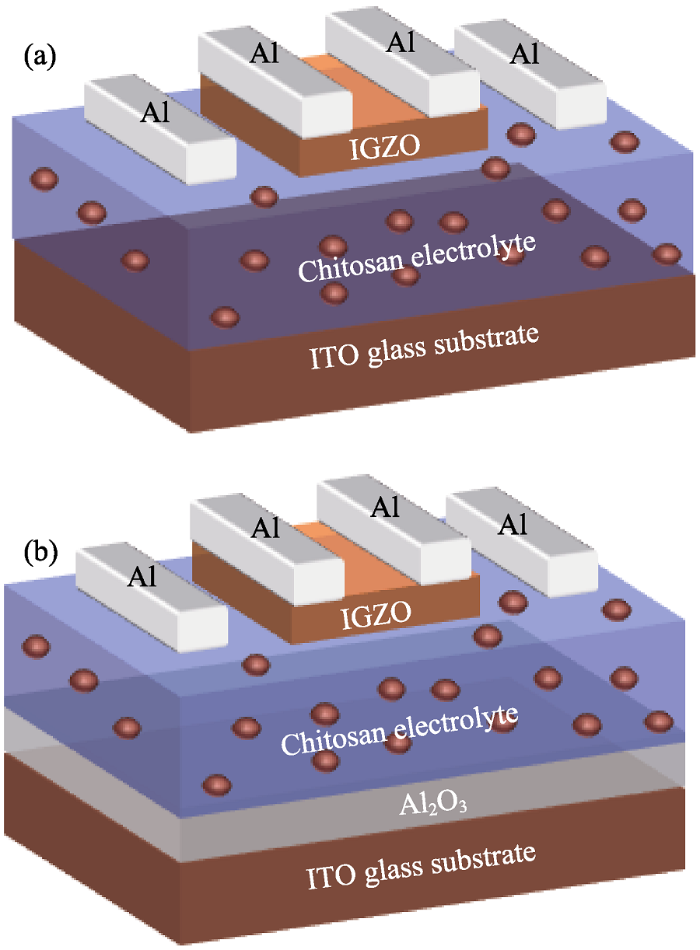
图1
基于不同介质的IGZO神经形态晶体管的结构图
Fig. 1
Schematic diagram of the IGZO-based neuromorphic transistor with different gate dielectrics
(a) Chitosan gate dielectric; (b) Stacked Al2O3/chitosan gate dielectrics
1.2 晶体管的表征和测试
采用原子力显微镜(AFM, Asylum Cipher) 表征栅介质的表面形貌, 并采用半导体参数分析仪(Keithley 2636B)和阻抗分析仪(HIOKI IM 3533-01 LCR meter)测试突触晶体管的电学性能和栅介质的电容特性。所有测试均在室温下进行。
2 结果与讨论
图2(a, b)的插图显示了壳聚糖栅介质和Al2O3膜的AFM形貌, 可以看出, 利用ALD制备的Al2O3薄膜相较于壳聚糖固体栅介质表面粗糙度更小, 形貌更加平整。平整的表面有利于改善界面接触, 最大限度减少缺陷、界面电荷和载流子的散射, 从而有助于构造具有更低亚阈值摆幅和更高电流开关比的高性能晶体管[28]。图2(a, b)给出了单层、双层栅介质的漏电流曲线, 即电流IG随栅极电压VG的变化曲线, 可以发现, Al2O3/壳聚糖叠层栅介质在1.8 V工作电压时产生约1.3 nA的漏电流, 与单层栅介质的漏电流(66.4 nA)相比, 减小了约98%。这是由于引入Al2O3层增大了栅介质层的物理厚度和绝缘性, 有效抑制了载流子隧穿电流, 从而大幅降低了漏电流, 这对于促进半导体的载流子输运、加强栅极对源漏电流的调控以及降低能耗至关重要, 同时也有利于减少后续突触塑性模拟过程中的非正常电流尖峰/毛刺[29-30]。图3(a, b)显示了两组不同结构IGZO晶体管的转移曲线, 其中器件线性区和饱和区的源漏电流(IDS)可用公式(1, 2)表示:
图2
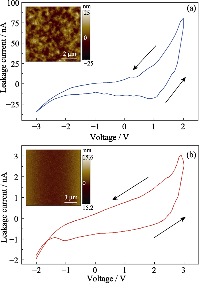
图2
单层、双层栅介质的漏电流曲线及其AFM形貌(插图)
Fig. 2
Leakage current curves and corresponding AFM images (inset) of monolayer gate dielectric and bilayer gate dielectric
(a) Chitosan solid dielectric; (b) Stacked Al2O3/chitosan bilayer gate dielectric (Inset: AFM image of Al2O3 membrane)
图3
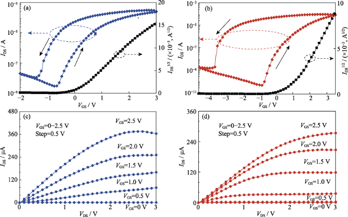
图3
两组不同结构IGZO晶体管的转移曲线和输出曲线
Fig. 3
Transfer characteristics and output characteristics of two kinds of dielectric devices
(a,b) Transfer characteristics of chitosan dielectric device (a) and stacked Al2O3/chitosan bilayer gate dielectric device (b); (c) Output characteristic of chitosan dielectric device; (d) Output characteristic of stacked Al2O3/chitosan bilayer gate dielectric device
其中, L表示沟道长度(80 μm), W表示沟道宽度(1000 μm), Ci为栅介质单位面积的电容(测试得到单层壳聚糖栅介质和叠层Al2O3/壳聚糖栅介质的Ci分别为2.23 和1.91 μF/cm2)。两组转移曲线均存在一个明显的逆时针滞回窗口, 这是由壳聚糖电解质中的离子迁移所致, 引入Al2O3加强了这一现象, 使逆时针滞回窗口宽度从1.10 V显著增大到3.73 V, 大的回滞窗口为后续突触功能模拟和神经形态系统的构建奠定了坚实的基础。表1汇总了两组晶体管的饱和迁移率、栅介质电容、电流开关比、亚阈值摆幅(SS)等基本性能参数[31]。晶体管的亚阈值摆幅由公式(3)估算得出。器件饱和迁移率μsat基于缓变沟道近似法和公式(4)给出。通过计算, 可以得出叠层Al2O3/壳聚糖栅介质器件的μsat为20.9 cm2·V-1·s-1, 与单层壳聚糖栅介质器件(18.0 cm2·V-1·s-1) 相比增长了16%。图3(c, d)是两组器件的输出曲线(栅电压VGS从0 V逐渐增加到2.5 V, 步长为0.5 V), 由图可见, 当VDS较低时, 两组器件均有明显的线性区域, 即具有良好的欧姆接触。不同的是, 加入Al2O3叠层的器件的输出曲线在饱和区域更加平直, 电流更加稳定, 这与Al2O3叠层对接触界面的改善有关。 综上所述, 添加Al2O3插入层后, 晶体管的漏电流、电流开关比、亚阈值摆幅、饱和迁移率和滞回窗口宽度等均有明显改善。
表1 两组IGZO神经形态晶体管的晶体管参数对比
Table 1
| Gate dielectric | Ioff | Ion/Ioff ratio | Subthreshold swing/ (mV·decade-1) | Hysteresis window/V | Leakage current (VG=1.8 V)/nA | μsat/ (cm2·V-1·s-1) |
|---|---|---|---|---|---|---|
| Chitosan | 2.92×10⁻⁹ | 1.06×10⁵ | 98.8 | 1.10 | 66.4 | 18.0 |
| Chitosan/Al2O3 | 4.20×10⁻¹¹ | 2.20×10⁶ | 78.3 | 3.73 | 1.3 | 20.9 |
此外, 还可以通过在调控栅极上施加电压来有效调制晶体管沟道层的电导[32], 这对于实现不同逻辑功能和降低系统功耗非常有意义。图4(a)是用光学显微镜拍摄的器件俯视图, 当G1作为栅电极, G2被施加不同幅值的调制电压时, 器件的电导和转移曲线特性会发生变化, 如图4(b)所示。器件的阈值电压(Vth)取值为(IDS)1/2与VG1的曲线与X轴的截距, 如图4(c)所示。当VG2=0时, 器件的Vth为0.7 V, 器件的关态电流约为4.20×10⁻¹¹ A,电流开关比约为2.20×10⁶。当VG2=1.0 V时, 器件的Vth为-0.56 V。通过观察, 得出的规律是:正调制电压会使器件的转移特性曲线向左偏移, 并使阈值电压降低;相反, 负调控电压则会使器件向右偏移, 并使器件的阈值电压升高。这是因为负调制电压会进一步促进沟道的电子累积, 这种情况下需要更大的阈值电压使器件导通。以上器件特性对于在单个器件上实现多逻辑功能非常有意义, 有助于灵活调节器件电流并降低大规模集成电路的面积和功耗。
图4
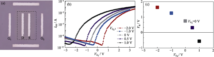
图4
晶体管的顶部光学显微镜照片(a), 在不同VG2下(范围为-2.0 V至1.0 V)的晶体管转移曲线(b)及不同VG2下的器件阈值电压变化(c)
Fig. 4
(a) Top micrograph, (b) transfer characteristics with different VG2 (from-2.0 V to 1.0 V) and (c) the Vth with different VG2 of transistor
神经元和突触是人脑中最重要且基本的组成部分, 人脑中数百亿个突触和神经元相互连接, 从而实现信息传递和整合。图5(a)显示了生物突触的简化示意图, 生物突触由突触前膜、突触后膜及突触间隙组成。当突触前膜受到生物脉冲刺激后, 会产生相应的动作电位开启钙离子输运通道, 钙离子在突触间隙中扩散并使得突触释放出神经递质, 然后与突触后膜上的受体相结合, 这个过程会产生突触后神经元兴奋电流, 称为兴奋性突触后电流(EPSC)。在本研究中, 突触前刺激通过在晶体管栅极上施加电压脉冲来模拟, 突触后电流则通过源漏电流读取。对于单层栅介质晶体管而言, 当在栅极施加突触前脉冲(0.5 V, 20 ms)并在源漏极施加读取电压时(VDS=0.1 V), 阳离子开始定向移动, 在沟道/栅介质界面处积累, 最终形成巨大的双电层电容并产生一个约24 nA的EPSC峰值, 脉冲结束后, 阳离子慢慢扩散回原位, 使得沟道电流回复稳定, 这个过程大约需要数秒。测试获得的EPSC峰值是栅漏电流、源漏电流以及寄生电容充放电电流叠加后的最终值。如图5(b)所示, 单层壳聚糖栅介质器件由于漏电流较大且较难抵消, 器件在EPSC产生前会产生异常电流尖峰, 即一个约为-5 nA的负向电流尖峰, 这明显不利于突触功能的稳定模拟。在发生这种情况时, 通常会通过增大脉冲幅值或源、漏读取电压来覆盖漏电流, 而这不利于降低功耗和精准模拟突触塑性。对于以Al2O3/壳聚糖为叠层栅介质的晶体管而言, 在同样的测试条件下, 器件的漏电明显降低, 这有利于在更低电压脉冲和源漏电压条件下避免异常电流尖峰的出现。此外, 叠层器件产生的EPSC峰值为0.86 nA, 远远低于单层壳聚糖栅介质器件(24 nA, 降低约97%), 则单脉冲刺激所产生的能耗也会大幅降低, 这对于构建低功耗神经形态系统非常有意义。 通过查阅文献, 本课题组汇总了不同结构神经形态晶体管的EPSC数据, 如表2所示, 相比之下, 本研究的晶体管产生的电流幅值(0.86 nA)远远小于其他结构的器件, EPSC行为的能耗也将有所降低。其中, 单脉冲EPSC行为的能耗根据公式(5)估算。
图5
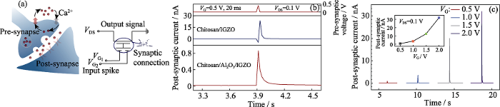
图5
(a) 生物突触结构示意图以及叠层Al2O3/壳聚糖栅介质突触晶体管的等效电路图, (b) 0.5 V, 20 ms电脉冲下的两组器件的EPSC响应, (c) 叠层Al2O3/壳聚糖栅介质晶体管在不同振幅的电脉冲诱发的EPSC
Fig. 5
(a) Schematic diagram of biological synapse and their equivalent electrical circuit of the neuromorphic transistor, (b) EPSC responses under an electric pulse of 0.5 V, and (c) EPSC induced by electric pulses of different amplitudes for IGZO-based dual-gate transistor with stacked Al2O3/chitosan gate dielectrics
表2 不同结构的人工突触晶体管的EPSC能耗对比
Table 2
| Structure | VDS/V | VG pulse | EPSC/nA | Energy consumption/(pJ·spike-1) | Ref. |
|---|---|---|---|---|---|
| Nanogranular SiO2/IZO | 1.0 | 0.8 V, 20 ms | 5000 | 105 | [33] |
| GO+Chitosan/IGZO | 0.1 | 0.5 V, 20 ms | 14 | 28 | [34] |
| Carbon Nanotube (CNT) | 0.5 | 4.0 V, 1.0 ms | 15 | 7.5 | [35] |
| Chitosan/IZO | 0.1 | 0.5 V, 25 ms | 2.6 | 6.5 | [36] |
| Chitosan/IWO | 0.1 | 0.2 V, 20 ms | 4.7 | 9.4 | [37] |
| Chitosan/IGZO | 0.1 | 0.5 V, 20 ms | 26 | 52 | [38] |
| Tungsten oxide | 0.3 | 0.6 V, 70 ms | 3.8 | 79 | [39] |
| Chitosan/ IGZO | 0.1 | 0.5 V, 20 ms | 24 | 48 | This work |
| Chitosan/Al2O3/IGZO | 0.1 | 0.5 V, 20 ms | 0.86 | 1.7 | This work |
此外, 如图5(c)所示, 当叠层栅介质晶体管栅极所加脉冲幅值变化时, EPSC峰值也会发生变化, 这与生物突触对不同强度刺激的反应不同相类似, 是短程突触可塑性的重要表现。多脉冲易化是神经形态计算系统处理时序信息的关键原理之一[40]。如图6(a)所示, 当连续八个脉冲(0.5 V, 25 ms)刺激叠层栅介质晶体管栅极时, 第八个脉冲引发的EPSC的幅值(A8)约为第一个刺激(A1)的5.5倍, 即易化率A8/A1为552%。这是因为当第一个脉冲刺激过后, 电解质中的质子会发生扩散, 经一定弛豫时间后恢复平衡位置, 当多个脉冲之间的时间间隔小于质子的弛豫时间时, 残余未恢复的质子会与后一个脉冲激发的质子叠加, 从而使得EPSC幅值增加, 这是多脉冲易化的产生机制。为进一步调控多脉冲易化, 可以改变脉冲的间隔时间, 图6(b)显示了突触晶体管的易化率随脉冲时间间隔的变化趋势, 随着脉冲间隔延长, 扩散回平衡位置的质子比例增大, 则易化率逐渐降低, 最终趋于100%。根据以上现象可以设计一个基于叠层Al2O3/壳聚糖栅介质突触晶体管的信号滤波器, 当信号频率高于1 Hz时, 器件会产生EPSC增强响应, 且增强幅度随信号频率增加而增加;当信号频率低于1 Hz时, 则对刺激信号产生屏蔽效应。上述结果均表明, 叠层栅介质晶体管可以较好地模仿EPSC和多脉冲易化等生物突触功能, 为后续模拟更多突触功能和构建神经形态系统奠定了基础。
图6
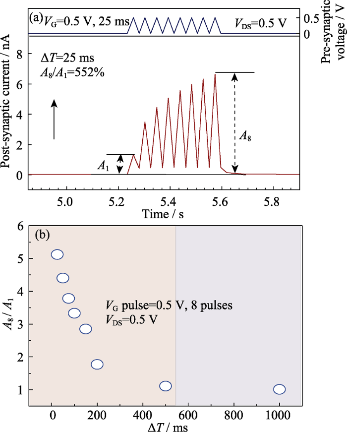
图6
叠层Al2O3/壳聚糖栅介质晶体管的(a)八个连续电脉冲(0.5 V, 25 ms)激发的多脉冲易化现象和(b) A8/A1的比值与脉冲时间间隔的关系图
Fig. 6
(a) Multi-pulse facilitation induced by eight successive electric pulse (0.5 V, 25 ms) and (b) ratio of A8/A1 plotted as a function of the time interval between the pulses for IGZO-based dual-gate transistor with stacked Al2O3/chitosan gate dielectrics
3 结论
本研究研制了一种采用Al2O3/壳聚糖叠层栅介质的新型IGZO神经形态晶体管。通过对比发现, 采用叠层栅介质的器件具有78.3 mV/decade的低亚阈值摆幅, 在1.8 V工作电压下1.3 nA的低漏电流(降低约98%), 3.73 V的大滞回窗口(提升4.3倍)以及0.86 nA的低兴奋性突触后电流(降低约97%), 单脉冲(0.5 V, 20 ms)功耗为1.7 pJ(降低约96%)。此外, 研究还利用双电层效应及双栅协同调控实现了电流的有效调控和突触尖峰功能的模拟, 并有效规避突触塑性模拟中由于高漏电导致的非正常电流尖峰。上述这些结果表明, 添加高k栅介质叠层对改善神经形态器件的漏电、功耗和性能大有帮助, 为进一步开发超功耗的神经形态感知与计算系统提供了有效技术途径。
参考文献
Towards spike-based machine intelligence with neuromorphic computing
Neuro-inspired computing with emerging nonvolatile memorys
Training and operation of an integrated neuromorphic network based on metal-oxide memristors
Recent advances in emerging neuromorphic computing and perception devices
Mott memory and neuromorphic devices
Long-term depression mimicked in an IGZO-based synaptic transistor
3-D stacked synapse array based on charge-trap flash memory for implementation of deep neural networks
Advanced multimaterial electronic and optoelectronic fibers and textiles
Semiconducting nanowire-based optoelectronic fibers
Orientation selectivity in a multi-gated organic electrochemical transistor
Ferroelectric analog synaptic transistors
Photoelectric synapse based on InGaZnO nanofibers for high precision neuromorphic computing
A spiking stochastic neuron based on stacked InGaZnO memristors
Ultralow-voltage transparent electric-double-layer thin-film transistors processed at room-temperature
Organic electronics for neuromorphic computing
Electric-double-layer transistors for synaptic devices and neuromorphic systems
Dual-functional long-term plasticity emulated in IGZO-based photoelectric neuromorphic transistors
Modulation of synaptic plasticity mimicked in Al nanoparticle-embedded IGZO synaptic transistor
Indium-gallium-zinc-oxide thin-film transistors: materials, devices, and applications

Since the invention of amorphous indium–gallium–zinc–oxide (IGZO) based thin-film transistors (TFTs) by Hideo Hosono in 2004, investigations on the topic of IGZO TFTs have been rapidly expanded thanks to their high electrical performance, large-area uniformity, and low processing temperature. This article reviews the recent progress and major trends in the field of IGZO-based TFTs. After a brief introduction of the history of IGZO and the main advantages of IGZO-based TFTs, an overview of IGZO materials and IGZO-based TFTs is given. In this part, IGZO material electron travelling orbitals and deposition methods are introduced, and the specific device structures and electrical performance are also presented. Afterwards, the recent advances of IGZO-based TFT applications are summarized, including flat panel display drivers, novel sensors, and emerging neuromorphic systems. In particular, the realization of flexible electronic systems is discussed. The last part of this review consists of the conclusions and gives an outlook over the field with a prediction for the future.
Amorphous InGaZnO (a-IGZO) synaptic transistor for neuromorphic computing
A non-volatile organic electrochemical device as a low-voltage artificial synapse for neuromorphic computing
The brain is capable of massively parallel information processing while consuming only similar to 1-100 fJ per synaptic event(1,2). Inspired by the efficiency of the brain, CMOS-based neural architectures(3) and memristors(4,5) are being developed for pattern recognition and machine learning. However, the volatility, design complexity and high supply voltages for CMOS architectures, and the stochastic and energy-costly switching of memristors complicate the path to achieve the interconnectivity, information density, and energy efficiency of the brain using either approach. Here we describe an electrochemical neuromorphic organic device (ENODe) operating with a fundamentally different mechanism from existing memristors. ENODe switches at low voltage and energy (<10 pJ for 10(3) mu m(2) devices), displays >500 distinct, non-volatile conductance states within a similar to 1V range, and achieves high classification accuracy when implemented in neural network simulations. Plastic ENODes are also fabricated on flexible substrates enabling the integration of neuromorphic functionality in stretchable electronic systems(6,7). Mechanical flexibility makes ENODes compatible with three-dimensional architectures, opening a path towards extreme interconnectivity comparable to the human brain.
Nanoelectronic programmable synapses based on phase change materials for brain-inspired computing
Brain-inspired computing is an emerging field, which aims to extend the capabilities of information technology beyond digital logic. A compact nanoscale device, emulating biological synapses, is needed as the building block for brain-like computational systems. Here, we report a new nanoscale electronic synapse based on technologically mature phase change materials employed in optical data storage and nonvolatile memory applications. We utilize continuous resistance transitions in phase change materials to mimic the analog nature of biological synapses, enabling the implementation of a synaptic learning rule. We demonstrate different forms of spike-timing-dependent plasticity using the same nanoscale synapse with picojoule level energy consumption.
Gate dielectric microstructural control of pentacene film growth mode and field-effect transistor performance
High-k gate dielectrics for emerging flexible and stretchable electronics
Solution-processed chitosan-gated IZO-based transistors for mimicking synaptic plasticity
Breakdown enhancement and current collapse suppression in AlGaN/GaN HEMT by NiOX/ SiNX and Al2O3/SiNX as gate dielectric layer and passivation layer
Extended gate ion-sensitive field-effect transistors using Al2O3/hexagonal boron nitride nanolayers for ph sensing
Surface/ interface roughness effects on magneto-electrical properties of thin films
Effect of composition, interface, and deposition sequence on electrical properties of nanolayered Ta2O5-Al2O3 films grown on silicon by atomic layer deposition
Electrical properties of ZnO nanowire field effect transistors with varying high-k Al2O3 dielectric thickness
Oxide semiconductor thin-film transistors: a review of recent advances
Chitosan-based electrolyte gated low voltage oxide transistor with a coplanar modulatory terminal
Biological band-pass filtering emulated by oxide-based neuromorphic transistors
Low-voltage oxide-based synaptic transistors for spiking humidity detection
A carbon nanotube synapse with dynamic logic and learning
Synaptic metaplasticity emulation in a freestanding oxide-based neuromorphic transistor with dual in-plane gates
Synaptic plasticity is a basic characteristic of synapses and plays an important role in the computation, learning and memory of human brain. Metaplasticity is a higher-order form of synaptic plasticity, which regulates the ability of synapses to generate synaptic plasticity and has a great regulating effect on later learning, memory and coping behaviors. At present, there are rarely reports on the emulation of synaptic metaplasticity in synaptic transistor. In this article, flexible dual-gate indium-zinc-oxide neuromorphic devices on freestanding solid-state proton conducting chitosan electrolyte membrane are designed for metaplasticity emulation. The key synaptic plasticity functions including excitatory postsynaptic current, synaptic paired-pulse response and synaptic pulse train response can be effectively regulated by the priming pulse stimuli. Besides, configurable synaptic depression and synaptic potentiation effect can be realized in such device. These results can expand the potential applications of the multi-terminal electrolyte-gated oxide transistors for flexible dynamic neuromorphic platforms.
Synaptic plasticity and classical conditioning mimicked in single indium-tungsten-oxide based neuromorphic transistor
Emulation of synaptic function by ionic/electronic hybrid device is crucial for brain-like computing and neuromorphic systems. Electric-double-layer (EDL) transistors with proton conducting electrolytes as the gate dielectrics provide a prospective approach for such application. Here, artificial synapses based on indium-tungsten-oxide (IWO)-based EDL transistors are proposed, and some important synaptic functions (excitatory post-synaptic current, paired-pulse facilitation, filtering) are emulated. Two types of spike-timing-dependent plasticity (Hebbian STDP and anti-Hebbian STDP) learning rules and multistore memory (sensory memory, short-term memory, and long-term memory) are also mimicked. At last, classical conditioning is successfully demonstrated. Our results indicate that IWO-based neuromorphic transistors are interesting for neuromorphic applications.
Oxide synaptic transistors coupled with triboelectric nanogenerators for bio-inspired tactile sensing application
Artificial synapses emulated by an electrolyte-gated tungsten-oxide transistor
