

随着科技水平不断提高, 人类社会逐步向信息化时代迈进。自从第一台计算机问世以来, 以金属-氧化物-半导体场效应晶体管(MOSFETs)作为集成电路核心器件的计算机结构为现代化信息社会奠定了基础。在过去的几十年里, 半导体电子器件的几何尺寸微缩一直遵循摩尔定律。面对数据处理速度需求不断增长, 提升计算机信息处理能力已经难以维持过去的速度。其中一个主要原因是传统的计算机采用冯·诺依曼架构, 分离的内存和中央处理器(CPU)通过总线进行数据读取和存储。在这些计算机中, 较高的计算速度要求数据异常频繁地在物理上分离的内存单元和处理单元之间传输, 对能源效率和数据带宽造成相当大的损伤, 这种现象通常被称为冯·诺依曼瓶颈。同时, 存储单元的读写速度和处理单元的计算速度之间的差距越来越大, 使得具有高计算速度的处理器要花费更多的时间等待数据读取完成后才能进行计算(存储墙)。存储墙的出现也使得冯·诺依曼瓶颈急速加剧, 最终限制了计算机信息处理能力的提升。
为了打破冯·诺依曼瓶颈, 研究者们受具有高度并行计算和自适应学习能力的人脑工作原理的启发, 提出了存算一体结构。新的计算架构也对硬件结构提出了新的要求, 存算一体器件需要在单一器件上同时实现计算和存储的功能, 进而模拟人脑的信号传输和处理方式。1971年, 加州大学伯克利分校蔡少棠教授从电路理论完备性出发提出了忆阻器的概念[1]。直到2008年, 惠普实验室Williams小组首次在单一器件中实现忆阻现象, 也正式宣布实现了忆阻器[2]。现如今忆阻器被证实非常适合作为存算一体架构的核心器件。忆阻器的电阻状态取决于施加的电压偏置过程, 器件可以基于不同的电阻阻值来存储信息, 同时实现存储和计算的功能。由忆阻器构成的交叉阵列(G)提供了全新的计算模式, 当读取电压(V)施加到忆阻器阵列上并读取电流(I)后, 电路就在物理意义上完成了一次I=G·V的矩阵运算。与传统计算机的基础加法运算相比, 矩阵计算极大地提高了运算的速度, 降低了运算的难度, 实现了更高的能量效率和更为复杂的数值计算。另外, 忆阻器具有类似于神经元和突触信号传输的非线性电学特性, 可以被应用于具有大脑神经功能的智能器件的研究和开发。忆阻器的诸多特性以及尺寸小、低运行功耗和高运行速度等特点为开发高效的神经形态计算和构建类脑神经网络提供了重要的解决方案, 在大数据处理、机器学习、模式识别和人工智能应用等方面均显示出巨大的潜力。
目前, 研究者们基于不同原理已经开发出多种不同结构的忆阻器, 如基于氧化还原反应和离子迁移的电化学氧化还原忆阻器[3⇓-5]、基于材料相变的相变忆阻器[6-7]、基于自旋极化隧穿效应的隧道磁阻忆阻器[8⇓-10]、基于铁电极化效应的铁电忆阻器[11-12]以及基于量子隧穿效应的浮栅忆阻器[13]等。特别是基于单介质层结构的忆阻器, 通常选取金属氧化物材料作为介质层, 制造成本低且具有良好的缩放前景, 并且十字交叉的集成方式为开发与CMOS工艺兼容的高密度忆阻器阵列提供了新的机会。但随着研究深入, 氧化物单介质层忆阻器表现出高低阻态不稳定、开关电压波动大和器件耐久性差等一系列问题, 阻碍了进一步开发和应用。在此基础上, 研究人员通过引入双介质层结构成功优化了氧化物忆阻器的结构和性能[14⇓-16]。本文对氧化物双介质层忆阻器的设计方案及其在类脑计算方面的应用进行论述, 首先介绍了氧化物双介质层忆阻器的结构和优势, 再从影响离子迁移的四个主要因素(电场强度、离子浓度、离子迁移势垒和焦耳热)出发, 综述了相关领域内氧化物双介质层忆阻器的阻变机理和设计思路, 最后讨论了氧化物双介质层忆阻器的应用和未来发展的机遇与挑战。
1 氧化物双介质层忆阻器的结构和优势
氧化物忆阻器开关参数的均匀性是考量器件性能的关键参数之一, 包括更为集中的开关电压范围和循环中高低电阻的稳定性以及耐久性等。这些性能参数则与导电细丝的生长和熔断密切相关, 后者的难易程度决定了忆阻器开关电压的大小, 导电细丝生长的直径与熔断的区域则影响了器件的开关电阻值。并且, 由于氧化物单介质层中电场均匀分布, 而大部分的氧化物层都是非晶的, 非晶材料的无序结构使得导电细丝的生长和熔断都具有很强的随机性, 进而导致氧化物单介质层忆阻器开关电压不稳定, 如图1(a, b)所示[17]。重复的直流I-V循环以及连续的脉冲操作会导致导电细丝变厚以及离子的不可逆迁移, 使绝缘体中金属或氧空位不断积累, 绝缘性质变差, 从而使氧化物单介质层忆阻器的高低阻态不稳定, 耐久性较差, 如图1(c)所示[18]。此外, 氧化物单介质层忆阻器中不规律的反向导通现象也极大降低了器件的可靠性。为了优化忆阻器的性能, 研究人员通过引入双介质层结构作为器件功能层, 利用一层氧化物薄膜作为阻变层, 通过调控其厚度和材料的性质, 限制导电细丝生长的长度以及熔断区域, 以稳定器件的高低电阻值; 而另一层氧化物薄膜则作为控制层或存储层, 在其中形成的锥形导电细丝可以集中电场, 限制阻变层中导电细丝的生长位置(图1(d)), 使忆阻器具有更稳定的开关特性, 如图1(e)所示。对于基于氧空位迁移的忆阻器器件, 存储层是缺氧的氧化物层或局部区域, 较多的氧空位为复位过程提供缓冲, 有效降低了器件反向击穿的风险, 从而提高了器件的可靠性。对基于金属离子迁移的忆阻器器件, 存储层包括活性电极和从其延伸出的突起, 通过调控存储层氧化物材料的物质特性, 可以抑制金属在阻变层中过度沉积, 有效延长器件的使用寿命, 如图1(f)所示。
图1
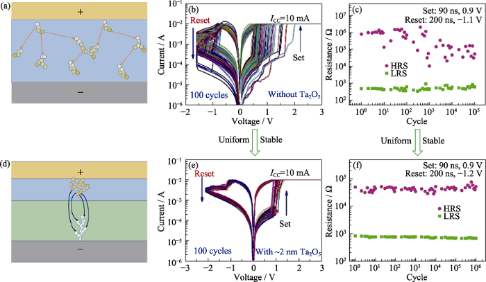
图1
氧化物双介质层忆阻器与氧化物单介质层忆阻器的结构和性能对比
Fig. 1
Comparison of the structure and performance between the single/double dielectric layer metal-oxide memristor
(a, d) Schematic diagrams for (a) single and (d) double dielectric layer metal-oxide memristors; (b, e) Comparison of I-V curves between (b) ZrO2-based memristor and (e) Ta2O5/ZrO2-based memristor with bi-layer structure exhibiting more uniform switching voltage[17]; (c, f) Comparison of the endurance between (c) HfO2-based memristor and (f) HfO2:Al/HfO2-based memristor with double dielectric layer exhibiting better cycling endurance[18]
表1 氧化物单介质层忆阻器与氧化物双介质层忆阻器性能参数对比
Table 1
| Memristor structure | Range of Set voltage, ΔVSet/V | Range of Reset voltage, ΔVReset/V | Endurance | On/Off ratio | Retention/s | Ref. | |
|---|---|---|---|---|---|---|---|
| Single dielectric layer | Ta/ZrO2/TiN | -1.0 ~-1.6 (0.6) | 0.8 ~ 1.5 (0.7) | 100 | 102 | - | [15] |
| Cu/Al2O3/Pt | 0.4 ~ 1.2 (0.8) | -0.1 ~-0.8 (0.7) | 2×10³ | 105 | 105 | [19] | |
| Ag/ZnO/Pt | 0.3 ~ 1.0 (0.7) | -0.4 ~-0.8 (0.4) | 102 | 50 | 104 | [20] | |
| TaN/Ta2O5/Pt | 2.0 ~ 4.5 (2.5) | -2.5 ~-4.5 (2) | 104 | - | 104 | [21] | |
| Ta/ZrO2/Pt | 0.4 ~ 2.0 (1.6) | -0.4 ~-1.0 (0.6) | 100 | - | - | [22] | |
| Double dielectric layer | Ag/SiO2/Ta2O5/Pt | 0.14 ~ 0.24 (0.1) | -0.06 ~-0.14 (0.08) | 103 | 103 | 104 | [14] |
| Ta/ZrO2/ZTO/TiN | -0.8 ~-1.2 (0.4) | 0.8 ~ 1.2 (0.4) | 105 | 102 | 3×10³ | [15] | |
| Ta/Ta2O5/ZrO2/Pt | 0.7 ~ 1.2 (0.5) | -0.5 ~-0.8 (0.3) | 106 | 102 | 104 | [17] | |
| TaN/Ta2O5/WO3/Pt | 1.6 ~ 2.3 (0.7) | -1.9 ~-2.5 (0.6) | 109 | - | 106 | [21] | |
| Ti/HfO2/TiOx/Pt | -0.8 ~-1.1 (0.3) | 1.4 ~ 1.5 (0.1) | 107 | 103 | 105 | [23] | |
忆阻器的垂直结构非常适合采用十字交叉阵列的结构实现器件集成, 而这种结构可以根据所施加的脉冲特性调整电导值进行复杂的计算, 为制造大规模神经网络提供了独特的机会。但基于氧化物单介质层忆阻器的交叉阵列结构中存在较明显的漏电流, 对准确读取器件电阻状态提出了挑战。并且氧化物单介质层忆阻器在Set过程中通常需要设置限流, 以保护忆阻器中的氧化物层免受永久击穿。为了解决这些问题, 研究人员通常将每个忆阻器串联一个晶体管(1T1R结构)或者一个选择器(1S1R结构)作为交叉阵列的一个存储单元, 但是存储单元的尺度微缩和集成密度受限, 且电路的耗能较大, 如1T1R单元大小约2500 μm2, 并且器件需要达到毫西门子级的电导率[24-25]。而双介质层结构为忆阻器多种功能的实现提供了更多的设计方案。通过调节功能层材料的性质以及合理搭配电极与功能层之间的能带结构, 氧化物双介质层忆阻器可以实现自限流和自整流等功能(如图2(a)所示), 在构建高密度的无源交叉阵列方面占有很大的优势[26]。
图2
图2
氧化物双介质层忆阻器在构建神经网络方面的性能优势
Fig. 2
Advantages of the double dielectric layer metal-oxide memristor in building neural network
(a) I-V curves of Pt/Al2O3/TaOx/Ta memristor with self-rectifying characteristic[26]; (b) Comparison of the pulse response between the HfO2 and the AlOx/HfO2-based memristor[30]
此外, 在已被研究的各种神经网络算法中, 深度神经网络被认为是执行大规模并行运算最具前途的架构之一, 它采用矩阵乘法计算输出神经元值并通过反向传播算法更新突触权重。其中, 反向传播算法的效率与忆阻器在脉冲刺激下各个电导状态的高度线性和对称性密切相关, 可以减轻突触权重调整程序以及外围电路设计的负担[27⇓-29]。精准调控导电细丝的生长与熔断是实现线性对称的电导调制的关键。实际操作中电场是相对可控的, 但氧化物单介质层忆阻器缺少控制层集中电场以及阻变层抑制离子的迁移, 使电导值存在较大变化, 施加较少增强/抑制脉冲后发生突然的增大/减小[5]。相比之下, 氧化物双介质层忆阻器可以通过合理搭配阻变层与控制层的电场强度, 有效调制导电细丝的生长。进一步地, 可以通过调控阻变层离子的迁移势垒抑制离子的过度迁移, 从而获得稳定且可重复的电导值。这些条件使得器件获得更多的电导状态和更线性的脉冲响应[30], 如图2(b)所示, 使得构建可靠且高效的大规模硬件神经网络成为可能。
2 氧化物双介质层忆阻器设计
理解忆阻器阻变机理是设计器件结构和优化器件性能的关键。大量研究表明, 金属氧化物忆阻器的工作机理可以归结于氧化还原反应和离子迁移[31⇓⇓⇓-35]。在电场作用下, 忆阻器的氧化物层中金属离子迁移会导致导电细丝形成或熔断, 实现了器件在高低阻态之间的切换。而氧空位迁移形成导电细丝的本质在于形成了特殊化学计量比的氧化物, 其具有类似金属的导电性。器件导通后, 导电细丝呈现典型的圆锥形状, 而导电细丝的熔断则发生在较窄的尖端附近[36⇓-38]。离子迁移主要由四个因素驱动: 电场强度、离子浓度[39]、离子迁移势垒[40]和由焦耳热引起的温度梯度[41-42]。在此基础上, 氧化物双介质层忆阻器的设计思路就是利用不同氧化物材料和电极材料的物理性质调制器件的电场分布、热量的耗散以及离子的迁移势垒。金属阳离子几乎不可能穿透没有任何缺陷的材料, 例如银离子穿透无缺陷的单层二硫化钼所需的能量高达35.01 eV, 而穿透有缺陷的单层二硫化钼所需的能量只需1.81 eV[43]。相应地, 在电场作用下, 氧离子只有极低的概率被激发形成氧空位, 并且其迁移势垒很高[40]。但若氧离子周围存在氧空位, 它则不需要完全克服能量束缚就可以迁移到近邻氧空位的位置。因此可以等效地认为是氧空位在氧化物中迁移, 且氧空位会降低迁移势垒。掺杂金属或改变材料的化学计量比是调制材料氧空位缺陷的常用方法[44-45]。部分金属材料作为电极会促进氧空位在氧化物界面处的形成, 其迁移势垒与界面性质相关[40]。焦耳热耗散与电极厚度以及氧化物氧含量相关[41,46], 这样通过调控阻变层氧含量以及与其相邻的金属电极厚度, 就可以限制导电细丝的熔断区域。
2.1 构建局域化电场
氧化物双介质层忆阻器的设计关键在于精确控制导电细丝形成位置、尺寸和熔断程度。而氧化物层内的电场强度影响离子迁移, 因此在有限区域内集中电场是一种优化忆阻器性能的有效方法。2018年, Guo等[14]报道了一种Ag/SiO2/Ta2O5/Pt忆阻器, 其功能层由RF-SiO2层和RF-Ta2O5层组成, 如图3(a)所示。器件的电阻开关发生在Ta2O5层中, 而SiO2层则用作离子储存层和控制层, 并起到诱导导电细丝生长的作用。Ag/SiO2/Ta2O5/Pt忆阻器具有更低、更均匀的开关电压,更为稳定的高/低阻态电阻值, 更长的持续时间以及更好的开关耐久性, 如图3(b)所示。器件的优异性能来源于: 在形成过程中, 银离子在致密的SiO2层中的离子迁移率较低, 导致较高浓度的银离子集中在银电极附近, 有更高的概率克服成核障碍, 促使金属导电细丝在SiO2层中重复成核和增长, 从而形成较粗的倒锥形结构。由于尖端效应, 电场集中在导电细丝的尖端附近, 限制了Ta2O5层中导电细丝的生长区域, 进而使器件具有更均匀的开关电压。在连续的循环过程中, 导电细丝的形成和熔断被控制在超薄Ta2O5层上, 有效抑制了Ag在Ta2O5层中的过度积累, 使其具有更稳定的高/低阻态阻值以及更好的循环耐久性。同时Ta2O5层的离子迁移率和氧化还原率较高, 使得器件的开关电压较低。该研究展示了一种在电化学金属化忆阻器中引入双介质层的较典型的设计思路, 即采用一层较厚的、低离子迁移率和氧化还原率的氧化物薄膜抑制金属阳离子的迁移, 同时形成一个金属锥体集中电场并诱导导电细丝生长; 另一层采用具有较高离子迁移率和氧化还原率的超薄的氧化物薄膜作为器件的开关层, 限制导电细丝的熔断区域。
图3
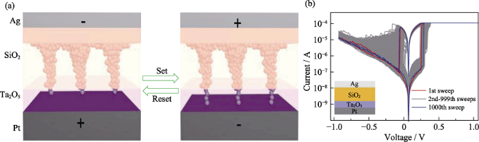
图3
基于电场局域化效应的氧化物双介质层忆阻器的机制与性能[14]
Fig. 3
Mechanism and characteristic of the double dielectric layer metal-oxide memristor based on the localization effect of electric field[14]
(a) Schematic illustration for the switching mechanism of Ag/SiO2/Ta2O5/Pt memristor; (b) I-V characteristic of Ag/SiO2/Ta2O5/Pt memristor
2.2 设计氧空位浓度梯度
基于氧空位迁移的氧化物双介质层忆阻器通常在氧空位浓度较高的氧化物薄膜中形成倒锥状的导电通道, 而氧空位浓度较低的氧化物薄膜则作为阻变层。2020年, Huang等[47]报道了一种W/AlOx/AlOy/Pt忆阻器, 功能层由RF-AlOx和ALD-AlOy组成, 其性能增强归因于氧空位缺陷浓度的差异, 如图4(a)所示。在形成过程中, 对W电极施加正偏压, 氧空位浓度较低的ALD-AlOy层电场强度更强。氧空位在浓度梯度和电场的驱动下在界面处迁移, 形成局部导电细丝, 进而诱导RF-AlOx层形成倒锥状导电细丝。倒锥状的导电细丝形成后, 由于氧空位浓度较低, ALD-AlOy层的电阻仍然大于RF-AlOx层, 因此电压主要落在ALD-AlOy层上。在此氧空位浓度梯度的影响下, 导电细丝的形成和破裂被限制在ALD-AlOy层中, 器件的开关参数表现出更高的均匀性。而界面处的氧空位浓度梯度, 有利于氧空位的层间迁移, 保证了工作电压较低, 降低了器件的功耗。这为设计基于氧空位迁移的氧化物双介质层忆阻器提供了参考, 即通过合理调配双介质层的氧空位浓度梯度诱导存储层中形成较稳定的倒锥状结构的导电细丝。氧空位较少的阻变层抑制导电细丝的径向扩散, 并且使电场集中分布在阻变层中, 促使导电细丝破裂得较为完全。依据这种设计思路, 提出了许多性能良好的双介质层氧化物忆阻器, 如Ta/Ta2O5/ZrO2/Pt[17]、Pt/TaOx/HfO2/Pt[48]、W/AlOx/Al2O3/Pt[49-50]、Pd/Ta2O5/TaOx/Pd[51]和ITO/ZnO/IGZO/ Al[52]等结构的忆阻器。
图4
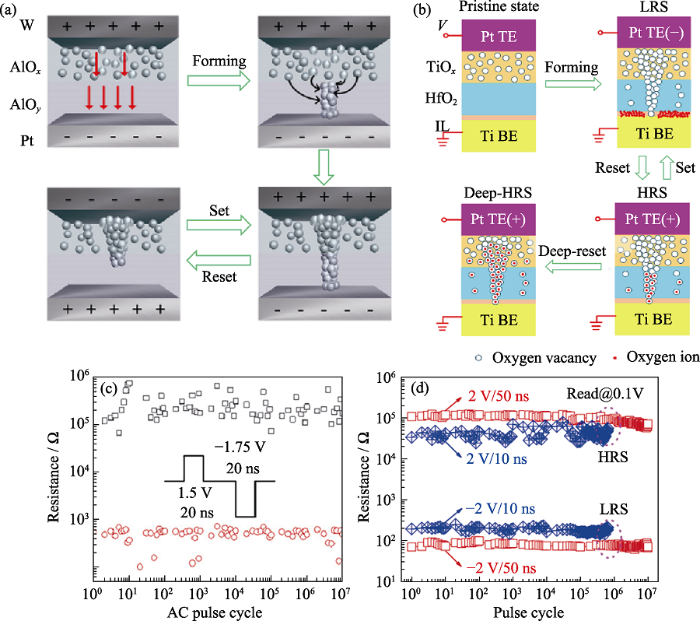
图4
基于氧空位梯度的氧化物双介质层器件的两种机制和性能对比
Fig. 4
Two mechanisms and characteristics comparison of the double dielectric layer metal-oxide memristor based on oxygen vacancy gradient
(a, b) Schematic diagrams of the resistance switching mechanism with (a) the structure of W/AlOx/AlOy/Pt memristor[47], (b) Ti/HfO2/TiOx/Pt memristor[23]; (c, d) Endurance of W/AlOx/AlOy/Pt memristor[47] and Ti/HfO2/TiOx/Pt memristor[23], and the Ti/HfO2/TiOx/Pt memristor with transition layer exhibiting more stable resistance states
Liu等[23]报道了一种类似的Ti/HfO2/TiOx/Pt忆阻器, 功能层由ALD-HfO2和ALD-TiOx组成, 如图4(b)所示。这种忆阻器具有自限流和深度复位的特性, 有利于在Set和Reset过程中保护器件免受永久故障。Ti/HfO2/TiOx/Pt忆阻器的电阻开关发生在HfO2层, 而TiOx层则作为串联电阻层和氧空位存储层, 不发生阻变。这种设计的关键在于, Ti电极和HfO2层之间形成了一个薄界面层, 用于存储Set过程中从HfO2层迁移的氧离子。在Set过程中, 氧空位浓度较高的TiOx层快速形成倒锥状导电通道, 诱导HfO2中导电细丝稳定生长。当器件导通后, TiOx层作为一层不发生阻变的固定的串联电阻值, 使器件导通后电阻始终大于这一固定电阻值, 降低了器件的工作电流, 实现自限流的功能。在Reset过程中, TiOx层可以存储多余的氧离子, 使器件具有深度复位的特性, 防止器件逆向导通。
对比上述两种器件, 可以发现功能层的设计都是采用相同的思路, 即利用氧空位浓度较高的存储层形成倒锥状导电细丝集中电场。但是在W/AlOx/AlOy/Pt忆阻器中, 氧空位浓度较高的存储层起到氧空位源的作用, 在Set过程中阻变层与存储层存在氧空位的交换, 而Ti/HfO2/TiOx/Pt忆阻器存储层则仅作为缓冲层, 在Reset过程中发挥作用。此外, 两种器件在测试过程中施加电压的方向是相反的, 其中关键在于Ti电极与HfO2层之间形成了缺氧的过渡层。对于氧化性较低的Pt电极, 施加正电压后, 氧离子将过度集中在电极与阻变层的界面, 阻碍了氧空位迁移与导电细丝的形成, 此时器件不发生阻变。而在相同情况下, 缺氧的过渡层则确保其中的氧离子可以在浓度梯度的驱动下径向迁移, 最终形成导电细丝。因此, 在氧化物双介质层忆阻器的设计中, 开关方向与电极选取紧密相关。这种采用氧浓度过渡层的设计方式, 异质氧化物界面在晶格应力的作用下将形成更多的氧空位, 而存储层与阻变层之间氧空位浓度差形成了较大的层间迁移势垒[53-54], 有效阻碍了氧离子的层间迁移, 使阻变层仅与过渡层存在氧离子交换, 形成了较为稳定的氧离子平衡。这些因素使得器件在循环中具有更稳定的电阻阻值, 如图4(c, d)所示, 这对双极型忆阻器非常重要。许多氧化物双介质层忆阻器也采用了这种设计方式, 常用于形成过渡层的电极有TiN[18]、TaN[21]、Ti[55-56]等。
2.3 降低焦耳热耗散
除了考虑电场和氧空位浓度对忆阻器性质的调控外, 电流流经导电细丝不可避免地会产生焦耳热, 其对导电细丝的形成和熔断同等重要。因此, 在设计氧化物双介质层忆阻器时还需要充分考虑局部焦耳热分布的影响。通过调控电极材料厚度或插入热增强层可以降低器件的热量耗散, 使导电细丝产生的焦耳热集中分布在开关层中, 并且促使温度在导电细丝的周围具有一定的梯度分布, 进而调控导电细丝的组分。对于不同的材料, 氧空位迁移形成导电细丝的组分是特定的, 不同组分可以为导电细丝提供不同的电导。例如, 对于Ta2O5材料, 导电细丝由非晶态的Ta(O)固溶体组成[39]; 对于HfOx材料, 导电细丝则是接近于金属的六方相结构, 如Hf2O、Hf3O、Hf6O等[33]。因此, 通过增强局部的焦耳热效应, 促使导电细丝的组分转变, 可以对器件开启时的电导状态进行调制。在此基础上, Mikhaylov等[57]基于夹在TiN/Ti和Au/Ta电极之间的双层ZrO2(Y)/Ta2O5介电质, 提出并实现了具有稳定非线性电导状态的氧化物双介质层忆阻器, 如图5(a)所示。器件设计的关键在于TiN/Ti电极附近形成的Ta纳米团簇作为热增强层, 使器件热导率降低, 限制了开关层的热量耗散并使导电细丝在开关层中发生较为彻底的溶解, 以形成更为稳定的低电导状态。并且, 温度沿径向呈一定梯度分布, 足够的热量促使导电细丝被一层非化学计量的氧化物包围。随着施加电场减小, 氧离子在导电细丝附近温度梯度的驱动下重新分布, 导电细丝的组分发生转变, 使器件高电导呈现非线性的特征, 如图5(b)所示。
图5
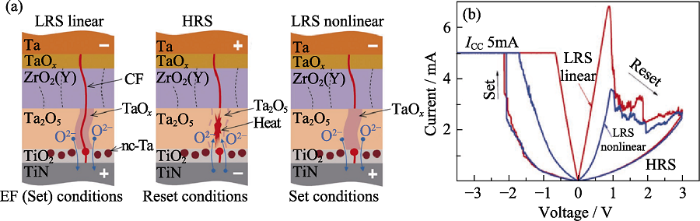
图5
基于焦耳热效应的氧化物双介质层忆阻器的机制与性能[57]
Fig. 5
Mechanism and performance of the double dielectric layer metal-oxide memristor based on Joule heating effect[57]
(a) Schematic diagrams of the switching mechanism of Ta/ZrO2(Y)/Ta2O5/TiN memristor; (b) I-V characteristic of Ta/ZrO2(Y)/Ta2O5/TiN memristor with nonlinear low-resistance state
2.4 调控离子迁移势垒
如前所述, 影响器件阻变机制的因素主要有电场、离子浓度梯度和焦耳热。在倒锥状导电细丝的影响下, 实际操作中电场是相对可控的。通过减少阻变层缺陷并选取价键更稳定的材料, 调控离子的迁移势垒, 可以抑制径向离子扩散与过度沉积, 促使导电细丝在施加电场的作用下生长和破裂, 以达到器件脉冲可控以及电导状态可重复的目的。2021年, Bousoulas等[58]提出的结构为Ag/SiO2/VOx/Pt的忆阻器就采用了这样的设计思路。如图6(a)所示, SiO2层中倒锥状导电细丝的形成使VOx层电场强度增强并集中在有限区域, 在保证开关均匀性的同时增强了电场对导电细丝的调控。银离子在VOx膜中的离子迁移势垒较高使器件电导变化具有高稳定性和可重复性, 从而促使Ag/SiO2/VOx/Pt忆阻器在连续相同的开关脉冲刺激下具有更多的电导状态以及高度对称的线性脉冲响应, 如图6(b)所示。采用类似的设计思路, 提出了许多具有良好突触特性的器件, 如Ta/Ta2O5/ZrO2/Pt[22]、TiN/ Al2O3/TiO2-x/Ti[59]和Pt/TiOx/Al2O3/Pt[60]等忆阻器。
图6
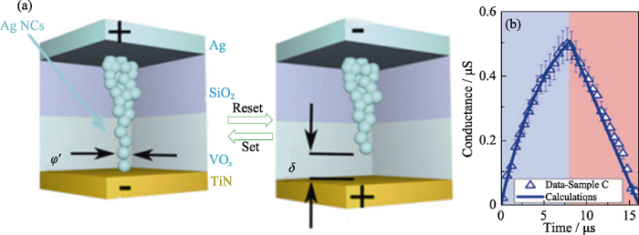
图6
氧化物双介质层忆阻器实现线性对称的脉冲响应的机制[58]
Fig. 6
Mechanism of the double dielectric layer metal-oxide memristor with the linear symmetrical pulse response[58]
(a) Schematic representation of the switching mechanism of Ag/SiO2/VOx/Pt memristor; (b) Pulse response of Ag/SiO2/VOx/Pt memristor represents highly linear and symmetric properties
3 氧化物双介质层忆阻器的应用
3.1 数据集分类
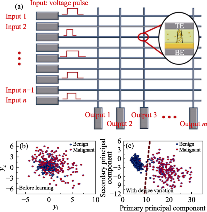
数据集分类是将数据的集合分组为由类似的对象组成的类别的分析过程, 通过检查输入变量之间的相关性来发现多元数据的相似因素。该技术还可用于降低输入数据的维数, 是许多机器学习算法的重要预处理步骤。相比氧化物单介质层忆阻器, 氧化物双介质层忆阻器具有更为稳定的开关参数以及线性对称的脉冲响应, 在提高分类效率的同时减轻了突触权重调整程序以及外围电路设计的负担。Choi等[51]基于Pd/TaOx/Ta2O5/Pd忆阻器构建了交叉阵列结构, 如图7(a)所示。在无监督的情况下, 通过利用桑格学习规则调整交叉阵列中每个忆阻器的权重。氧化物双介质层忆阻器交叉阵列网络可以实现在线学习, 通过训练可以从数据集中学习主成分, 并有效地将未标记的数据分成簇, 如图7(b)所示。在学习主成分后, 利用氧化物双介质层忆阻器网络先进行数据聚类并推导出数据集的分类, 然后得到线性决策边界, 如图7(c)所示。这种方法可以扩展到更大的网络和其他机器学习算法, 用于更复杂的数据密集型任务。
图7
3.2 语音识别
语音识别的目标是独立于说话者来区分语音的内容。因此, 音频信号的特征处理非常重要。相比于其他神经网络算法, 储备池算法是一种处理音频信号的高效网络, 只需要训练连接到输出层的权重, 网络的其余部分保持不变, 如图8(a)所示。因此, 训练过程变得线性, 可以使用许多简单的训练算法, 但需要硬件神经网络可以生成丰富的存储状态。在氧化物忆阻器中引入双介质层结构, 使得器件电导变化具有高稳定性和可重复性, 并且在连续相同的开关脉冲刺激下具有更多的电导状态。Zhong等[61]基于一种具有多电导状态的Ti/TiOx/TaOy/Pt忆阻器, 如图8(b)所示, 利用并行的储备池系统实现了语音识别的功能。研究表明, 基于氧化物双介质层忆阻器的储备池系统可以有效地处理时间信号, 实现语音数字识别的错误率仅为0.4%, 如图8(c, d)所示。这种并行的储备池系统是在一个以串行方式运行的单个器件上实现的, 证明了基于氧化物双介质层忆阻器神经形态计算的可行性和高效性。
图8
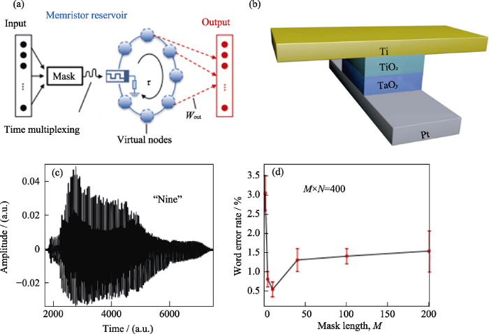
图8
氧化物双介质层忆阻器实现语音识别[61]
Fig. 8
Demonstration of speech recognition using double dielectric layer metal-oxide memristor[61]
(a) Schematic of the memristor-based reservoir computing system; (b) Diagram of Ti/TiOx/TaOy/Pt memristor structure; (c) Typical audio waveform of digit 9; (d) Recognition error rate of speech varies as a function of the mask length with error bar representing variation between memristor devices
3.3 图像识别
高密度的无源忆阻器交叉阵列可以将大型神经网络模型直接存储在专门的神经形态芯片上, 避免了芯片外编程, 使图像识别等算法具有更高的效率和更低的功耗。但基于氧化物单介质层忆阻器的交叉阵列结构中存在较明显的漏电流, 对器件电阻状态的准确读取提出了挑战。Kim等[59]利用TiN/ Al2O3/TiO2-x/Ti忆阻器构建的64×64的无源交叉阵列电路(图9(a)), 实现了数据的有效存储和准确读取并演示了较高精度地识别手写数字图像。电路的制备采用CMOS兼容的制造技术, 适用于三维集成和后端工艺, 在神经形态计算应用中具有广阔的前景。实验演示了一个平均相对电导输入精度为1%的64×10的矩阵乘法, 模拟了由非原位训练的单层感知器进行的MNIST图像分类, 如图9(b)所示。此外, Choi等[62]提出了一种具有自整流效应的Pt/TaOy/TaOx/Ta忆阻器, 搭建了16×16的交叉阵列结构并进行了手写数字的识别, 如图9(c)所示。利用这种氧化物双介质层忆阻器神经网络经15次迭代后识别MNIST数字图像, 其精度可以达到89.08%, 如图9(d)所示。这些研究结果表明, 氧化物双介质层忆阻器在实现人脑规模的整合神经形态系统方面具有极大潜力。
图9
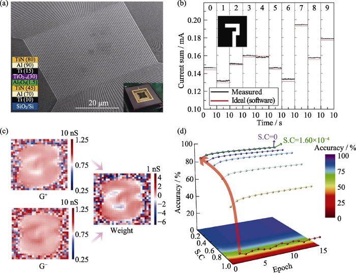
图9
氧化物双介质层忆阻器实现图像识别
Fig. 9
Demonstration of image recognition using double dielectric layer metal-oxide memristor
(a) SEM image of the 64×64 memristor crossbar array; (b) All experimental output currents for the digit “7”[59]; (c) Recognition diagrams of conductance and synaptic weights of digit “3”; (d) Evolution of the recognition accuracy of the MNIST under different synaptic coupling and training epochs[62]
4 结论与展望
氧化物双介质层忆阻器的开关电压均匀性、高低阻态稳定性和耐久性等比氧化物单介质层忆阻器显著提高。并且, 双介质层结构使得忆阻器具有线性对称的脉冲响应以及自限流、自整流等特性, 在构建无源交叉阵列以及神经形态计算方面具有明显优势。本文基于氧化物忆阻器的基本原理, 从影响离子迁移的四个主要因素: 电场强度、离子浓度、焦耳热和离子迁移势垒出发, 总结了几种性能良好的氧化物双介质层忆阻器的设计方法:
1)采用一层氧化物薄膜作为控制层, 形成一个稳定的倒锥状导电细丝集中电场并限制导电细丝的生长区域, 使器件的开关电压更均匀; 另一层超薄的氧化物薄膜则作为器件的开关层, 限制了导电细丝的熔断区域, 提高了器件的稳定性。
2)通过合理调配双介质层的氧空位浓度梯度, 诱导存储层中形成较稳定的倒锥状导电细丝。并选取氧化性较好的金属作为阻变层一侧的电极, 形成缺氧过渡层。这种采用氧浓度过渡层的设计方式, 确保了氧离子可以在浓度梯度的驱动下在过渡层中迁移。阻变层仅与过渡层存在氧离子交换, 达到较为稳定的平衡。再考虑到异质界面有效阻碍了氧离子的层间迁移。上述因素使氧化物双介质层忆阻器在循环中具有更稳定的高低电阻。
3)形成具有纳米团簇的热增强层, 限制开关层的热量耗散, 并使温度沿导电细丝径向具有一定的梯度分布, 足够的热量促使导电细丝被一层非化学计量的氧化物包围。随着施加电场减小, 氧离子在导电细丝附近温度梯度的驱动下重新分布, 导电细丝的组分发生转变, 使器件高电导呈现非线性的特征。
4)较低的离子迁移势垒会增大导电细丝生长的随机性, 可通过减少阻变层缺陷或选取价键更稳定的材料调控离子的迁移势垒, 抑制径向离子扩散与过度沉积, 促使导电细丝仅在电场的驱动下生长破裂, 以达到氧化物双介质层忆阻器脉冲电导状态线性可控的目的。
总的来说, 氧化物双介质层忆阻器的设计思路就是利用不同氧化物材料和电极材料的物理性质调制器件的电场分布、热量耗散和离子迁移势垒等, 以实现不同场景所需的多种性能, 为实现神经形态计算提供基础。
发展至今, 氧化物双介质层忆阻器仍然存在许多机遇与挑战。(1)氧化物双介质层忆阻器的优异性能与其电化学形成过程紧密相关, 导致器件间的开关参数存在一定差异。而一些不存在电化学形成过程的器件本质上也依赖于第一次I-V循环的设置。因此, 为实现高效可靠的神经形态计算, 迫切需要改进生产技术, 在提高产量的同时减少器件间参数的变化。从制备技术上出发, 可以采用制备锥状电极或掺杂纳米团簇等方式[63-64], 进一步优化氧化物双介质层忆阻器的开关参数与突触模拟特性。(2)有关氧空位迁移阻变机理的研究大多基于理论模拟, 实验观察较少。氧化物材料的不同参数, 如厚度、缺陷浓度和氧化还原性等因素, 对氧空位迁移形成导电细丝的具体影响有待实验的进一步验证。特别是氧化物双介质层忆阻器存在层间迁移, 层间迁移的势垒是影响沙漏型导电细丝生长的潜在因素, 决定了氧化物双介质层忆阻器导电细丝熔断的具体位置, 对其阻变机理的分析至关重要。(3)相关研究表明, 导电细丝焦耳热可以促使一些氧化物材料结晶, 限制导电细丝生长路径和尺寸, 从而获得稳定开关电压, 改善器件性能[33]。进一步地, 当导电细丝生长完成, 其产生的热量还将继续促进结晶过程, 使器件电导状态受脉冲数量的调控。从这样的思路出发, 将相变机理和导电细丝机理相互结合, 可以设计出具有多种功能的氧化物双介质层忆阻器。在本文总结的几种设计方法的基础上, 研究人员可以依据神经形态计算的不同需要, 结合多种物理原理, 设计出性能多样的新型忆阻器。
参考文献
Memristor-the missing circuit element
The missing memristor found
Cluster-type analogue memristor by engineering redox dynamics for high-performance neuromorphic computing
Short-term memory to long-term memory transition in a nanoscale memristor

"Memory" is an essential building block in learning and decision-making in biological systems. Unlike modern semiconductor memory devices, needless to say, human memory is by no means eternal. Yet, forgetfulness is not always a disadvantage since it releases memory storage for more important or more frequently accessed pieces of information and is thought to be necessary for individuals to adapt to new environments. Eventually, only memories that are of significance are transformed from short-term memory into long-term memory through repeated stimulation. In this study, we show experimentally that the retention loss in a nanoscale memristor device bears striking resemblance to memory loss in biological systems. By stimulating the memristor with repeated voltage pulses, we observe an effect analogous to memory transition in biological systems with much improved retention time accompanied by additional structural changes in the memristor. We verify that not only the shape or the total number of stimuli is influential, but also the time interval between stimulation pulses (i.e., the stimulation rate) plays a crucial role in determining the effectiveness of the transition. The memory enhancement and transition of the memristor device was explained from the microscopic picture of impurity redistribution and can be qualitatively described by the same equations governing biological memories.© 2011 American Chemical Society
Nanoscale memristor device as synapse in neuromorphic systems
A memristor is a two-terminal electronic device whose conductance can be precisely modulated by charge or flux through it. Here we experimentally demonstrate a nanoscale silicon-based memristor device and show that a hybrid system composed of complementary metal-oxide semiconductor neurons and memristor synapses can support important synaptic functions such as spike timing dependent plasticity. Using memristors as synapses in neuromorphic circuits can potentially offer both high connectivity and high density required for efficient computing.
Phase-change processors, memristors and memflectors
Memristive phase switching in two-dimensional 1T-TaS2 crystals
Non-volatile magnetic random access memories (MRAM)
Reliability study of perpendicular STT-MRAM as emerging embedded memory qualified for reflow soldering at 260 ℃
Current-induced spin-orbit torques in ferromagnetic and antiferromagnetic systems
Two-dimensional In2Se3: a rising advanced material for ferroelectric data storage
Ferroelectric thin films: review of materials, properties and applications
A high-on/off-ratio floating-gate memristor array on a flexible substrate via CVD-grown large-area 2D layer stacking
SiO2/Ta2O5 heterojunction ECM memristors: physical nature of their low voltage operation with high stability and uniformity
Stabilized and reset-voltage controlled multi-level switching characteristics in ZrO2-based memristors by inserting a-ZTO interface layer
Contact engineering approach to improve the linearity of multilevel memristive devices
Physical mechanisms underlying the multilevel resistive tuning over seven orders of magnitude in structures based on TiO2/Al2O3 bilayers, sandwiched between platinum electrodes, are responsible for the nonlinear dependence of the conductivity of intermediate resistance states on the writing voltage. To improve the linearity of the electric-field resistance tuning, we apply a contact engineering approach. For this purpose, platinum top electrodes were replaced with aluminum and copper ones to induce the oxygen-related electrochemical reactions at the interface with the Al2O3 switching layer of the structures. Based on experimental results, it was found that electrode material substitution provokes modification of the physical mechanism behind the resistive switching in TiO2/Al2O3 bilayers. In the case of aluminum electrodes, a memory window has been narrowed down to three orders of magnitude, while the linearity of resistance tuning was improved. For copper electrodes, a combination of effects related to metal ion diffusion with oxygen vacancies driven resistive switching was responsible for a rapid relaxation of intermediate resistance states in TiO2/Al2O3 bilayers.
Optimizing the thickness of Ta2O5 interfacial barrier layer to limit the oxidization of Ta ohmic interface and ZrO2 switching layer for multilevel data storage
Uniform and robust TiN/HfO2/Pt memristor through interfacial Al-doping engineering
Effects of heavy ion irradiation on Cu/Al2O3/Pt CBRAM devices
Low power consumption nanofilamentary ECM and VCM cells in a single sidewall of high-density VRRAM arrays
Flexible Ta2O5/WO3-based memristor synapse for wearable and neuromorphic applications
Emulating synaptic plasticity and resistive switching characteristics through amorphous Ta2O5 embedded layer for neuromorphic computing
An electronic synaptic device based on HfO2TiOx bilayer structure memristor with self-compliance and deep-RESET characteristics
Memristive crossbar arrays for brain-inspired computing
With their working mechanisms based on ion migration, the switching dynamics and electrical behaviour of memristive devices resemble those of synapses and neurons, making these devices promising candidates for brain-inspired computing. Built into large-scale crossbar arrays to form neural networks, they perform efficient in-memory computing with massive parallelism by directly using physical laws. The dynamical interactions between artificial synapses and neurons equip the networks with both supervised and unsupervised learning capabilities. Moreover, their ability to interface with analogue signals from sensors without analogue/digital conversions reduces the processing time and energy overhead. Although numerous simulations have indicated the potential of these networks for brain-inspired computing, experimental implementation of large-scale memristive arrays is still in its infancy. This Review looks at the progress, challenges and possible solutions for efficient brain-inspired computation with memristive implementations, both as accelerators for deep learning and as building blocks for spiking neural networks.
Post-moore memory technology: sneak path current (SPC) phenomena on RRAM crossbar array and solutions
Pt/Al2O3/TaOx/Ta self-rectifying memristor with record-low operation current (<2 pA), low power (fJ), and high scalability
In-memory learning with analog resistive switching memory: a review and perspective
NeuroSim+: an integrated device-to-algorithm framework for benchmarking synaptic devices and array architectures
Technological benchmark of analog synaptic devices for neuroinspired architectures
Improved synaptic behavior under identical pulses using AlOx/HfO2 bilayer RRAM array for neuromorphic systems
The mechanism of electroforming of metal oxide memristive switches
Oxygen migration around the filament region in HfOxmemristors
Nanoscale resistive switching devices: mechanisms and modeling
Resistive switching devices (also termed memristive devices or memristors) are two-terminal nonlinear dynamic electronic devices that can have broad applications in the fields of nonvolatile memory, reconfigurable logic, analog circuits, and neuromorphic computing. Current rapid advances in memristive devices in turn demand better understanding of the switching mechanism and the development of physics-based as well as simplified device models to guide future device designs and circuit-level applications. In this article, we review the physical processes behind resistive switching (memristive) phenomena and discuss the experimental and modeling efforts to explain these effects. In this article three categories of devices, in which the resistive switching effects are driven by cation migration, anion migration, and electronic effects, will be discussed. The fundamental driving forces and the stochastic nature of resistive switching will also be discussed.
2D materials and van der Waals heterojunctions for neuromorphic computing
Three-dimensional observation of the conductive filament in nanoscaled resistive memory devices
The basic unit of information in filamentary-based resistive switching memories is physically stored in a conductive filament. Therefore, the overall performance of the device is indissolubly related to the properties of such filament. In this Letter, we report for the first time on the three-dimensional (3D) observation of the shape of the conductive filament. The observation of the filament is done in a nanoscale conductive-bridging device, which is programmed under real operative conditions. To obtain the 3D-information we developed a dedicated tomography technique based on conductive atomic force microscopy. The shape and size of the conductive filament are obtained in three-dimensions with nanometric resolution. The observed filament presents a conical shape with the narrow part close to the inert-electrode. On the basis of this shape, we conclude that the dynamic filament-growth is limited by the cation transport. In addition, we demonstrate the role of the programming current, which clearly influences the physical-volume of the induced conductive filaments.
Observation of conducting filament growth in nanoscale resistive memories
Direct observations of nanofilament evolution in switching processes in HfO2 based resistive random access memory by in situ TEM studies
Anatomy of a nanoscale conduction channel reveals the mechanism of a high performance memristor
Direct measurement of nanoscale filamentary hot spots in resistive memory devices
The switching location of a bipolar memristor: chemical, thermal and structural mapping
Interface engineering via MoS2insertion layer for improving resistive switching of conductive bridging random access memory
Tailoring switching and endurance/retention reliability characteristics of HfO2/Hf RRAM with Ti, Al, Si dopants
Performance enhancement of TaOx resistive switching memory using graded oxygen content
Thermal transport in tantalum oxide films for memristive applications
Enhancement of DC/AC resistive switching performance in AlOx memristor by two technique bilayer approach
Resistive switching and synaptic plasticity in HfO2-based memristors with single-layer and bilayer structures
Forming-free, fast, uniform, and high endurance resistive switching from cryogenic to high temperatures in W/AlOx/Al2O3/Pt bilayer memristor
Low-power, high speed and high uniform switching in AlOx-based memristor using homogeneous bilayer structure for memcomputing
Data clustering using memristor networks
Resistive switching in sputtered ZnO/IGZO heterostructure memristor
Effect of oxide/oxide interface on polarity dependent resistive switching behavior in ZnO/ZrO2 heterostructures
Probing vacancy behavior across complex oxide heterointerfaces
Improving linearity by introducing Al in HfO2 as a memristor synapse device
A tantalum oxide memristor for artificial synapse applications
Multilayer metal-oxide memristive device with stabilized resistive switching
Tuning the analog synaptic properties of forming free SiO2 memristors by material engineering
4K-memristor analog-grade passive crossbar circuit
Memristor based on TiOx/Al2O3 bilayer as flexible artificial synapse for neuromorphic electronics
Dynamic memristor-based reservoir computing for high-efficiency temporal signal processing
A self-rectifying TaOy/ nanoporous TaOx memristor synaptic array for learning and energy-efficient neuromorphic systems
Fabrication of a Cu-cone-shaped cation source inserted conductive bridge random access memory and its improved switching reliability
Multi-level control of conductive filament evolution and enhanced resistance controllability of the Cu-cone structure embedded conductive bridge random access memory
