Journal of Inorganic Materials ›› 2020, Vol. 35 ›› Issue (5): 561-566.DOI: 10.15541/jim20190246
Special Issue: 功能陶瓷论文精选(一):发光材料
Previous Articles Next Articles
ZHENG Xue1,JIANG Rui1,LI Qian1,WANG Weizhe1,XU Zhimou1( ),PENG Jing2
Received:2019-05-24
Revised:2019-09-08
Published:2020-05-20
Online:2019-12-29
Supported by:CLC Number:
ZHENG Xue, JIANG Rui, LI Qian, WANG Weizhe, XU Zhimou, PENG Jing. Research on Anodic Aluminum Oxide Nanostructured LEDs[J]. Journal of Inorganic Materials, 2020, 35(5): 561-566.
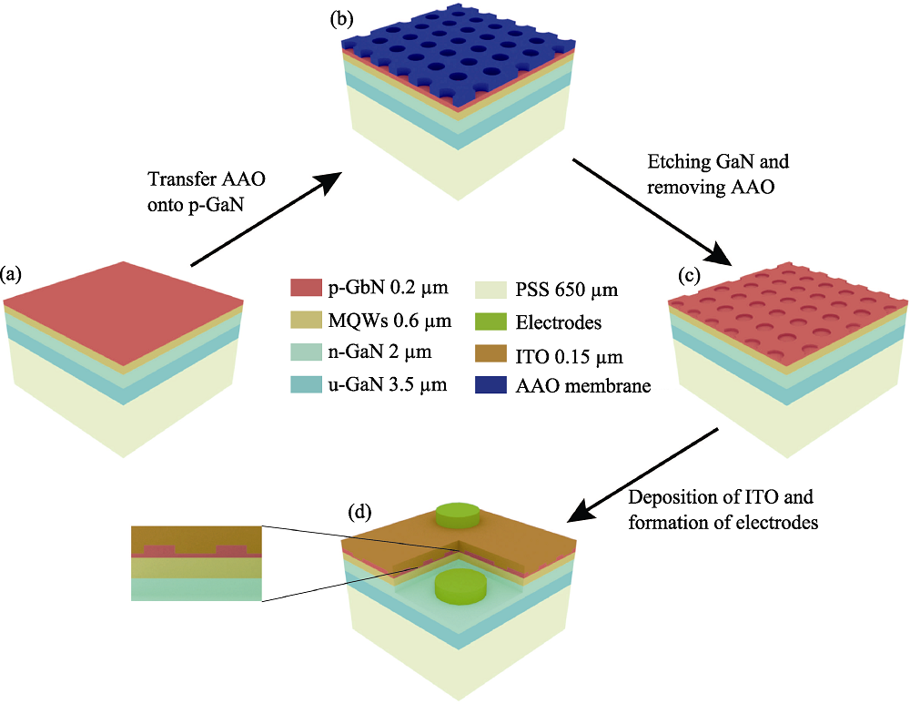
Fig. 1 Schematic of the fabrication process of nanostructured LED chip
| Materials | Gas flow/sccm | Pressure/Pa | Power/W | Time/s | |
|---|---|---|---|---|---|
| Al2O3 | BCl3 | 40 | 1.0664 | 400 | 240 |
| Ar | 10 | ||||
| GaN | BCl3 | 20 | 0.5332 | 550 | 25 |
| Cl2 | 30 | ||||
Table 1 Parameters of the ICP etching
| Materials | Gas flow/sccm | Pressure/Pa | Power/W | Time/s | |
|---|---|---|---|---|---|
| Al2O3 | BCl3 | 40 | 1.0664 | 400 | 240 |
| Ar | 10 | ||||
| GaN | BCl3 | 20 | 0.5332 | 550 | 25 |
| Cl2 | 30 | ||||
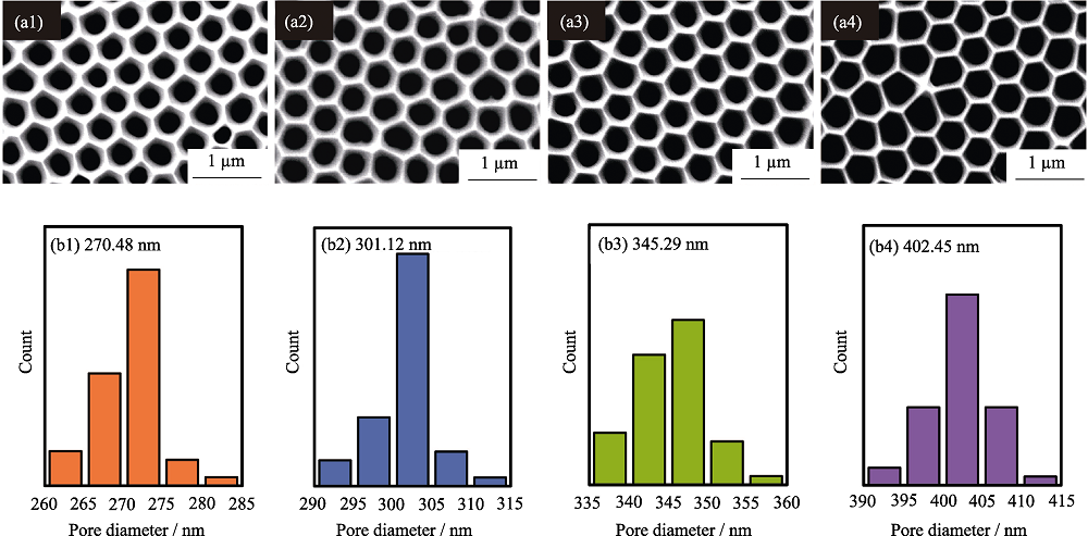
Fig. 2 SEM images of the AAO membrane which pore widening by increasing etching time and calculated scale distribution of the pore diameter in (a1-a4) (a1) 60 s; (a2) 120 s; (a3) 180 s; (a4) 240 s. (b1-b4) correspond to (a1-a4)
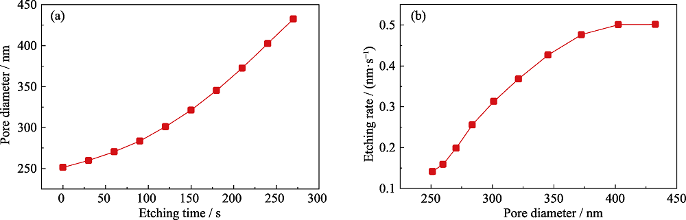
Fig. 3 Curve of the pore diameter with the etching time (a) and curve of the etching rate with the pore diameter (b)
| t/s | D/nm | V/(nm·s-1) |
|---|---|---|
| 0 | 251.37 | 0.141 |
| 30 | 259.85 | 0.159 |
| 60 | 270.48 | 0.199 |
| 90 | 283.70 | 0.255 |
| 120 | 301.12 | 0.313 |
| 150 | 321.28 | 0.368 |
| 180 | 345.29 | 0.426 |
| 210 | 372.45 | 0.476 |
| 240 | 402.45 | 0.500 |
| 270 | 432.53 | 0.501 |
Table 2 Statistics of pore diameter and etching rate with ICP etching for different durations
| t/s | D/nm | V/(nm·s-1) |
|---|---|---|
| 0 | 251.37 | 0.141 |
| 30 | 259.85 | 0.159 |
| 60 | 270.48 | 0.199 |
| 90 | 283.70 | 0.255 |
| 120 | 301.12 | 0.313 |
| 150 | 321.28 | 0.368 |
| 180 | 345.29 | 0.426 |
| 210 | 372.45 | 0.476 |
| 240 | 402.45 | 0.500 |
| 270 | 432.53 | 0.501 |
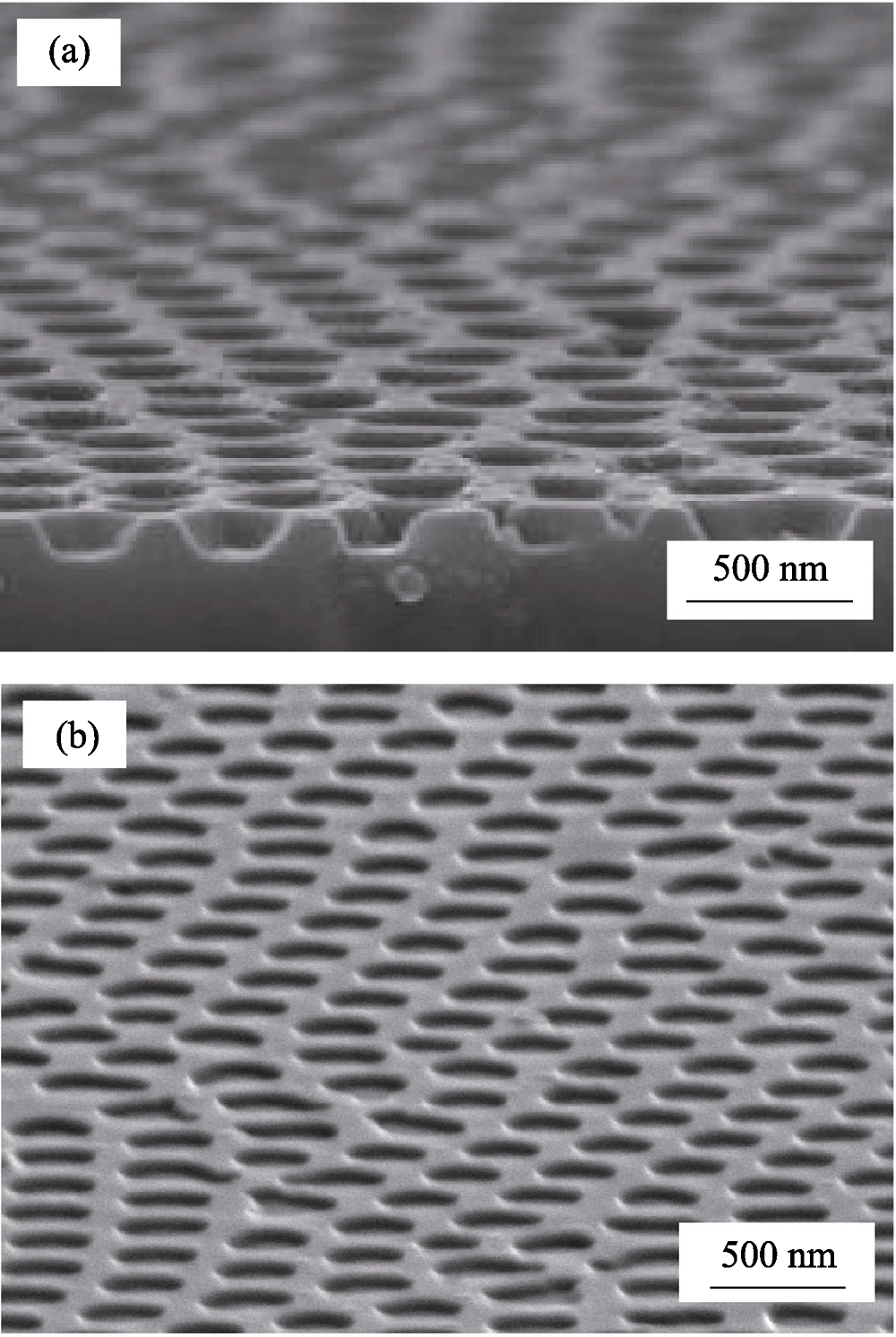
Fig. 4 SEM images of nanostructured LED chip (a) Cross sectional view; (b) Oblique view
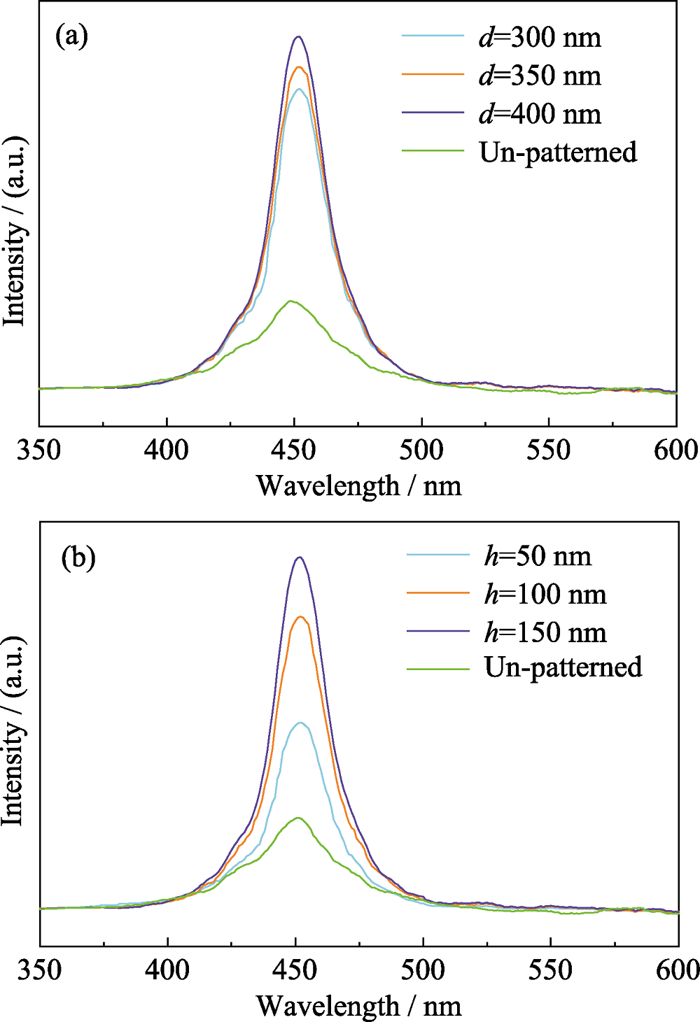
Fig. 5 PL spectra of nanostructured LEDs with different pore diameter (a) and different depths (b)
| [1] | CHO J, PARK J H, KIM J K , et al. White light-emitting diodes: history, progress, and future. Laser & Photonics Reviews, 2017,11(2):1600147. |
| [2] | LI Y, WANG W, HUANG L , et al. High-performance vertical GaN-based near-ultraviolet light-emitting diodes on Si substrates. Journal of Materials Chemistry C, 2018,6(42):11255-11260. |
| [3] | LUO X, HU R, LIU S , et al. Heat and fluid flow in high-power LED packaging and applications. Progress in Energy and Combustion Science, 2016,56:1-32. |
| [4] | FERREIRA R X G, XIE E, MCKENDRY J J D , et al. High bandwidth GaN-based micro-LEDs for multi-Gb/s visible light communications. IEEE Photonics Technology Letters, 2016,28(19):2023-2026. |
| [5] | CHO J, SCHUBERT E F, KIM J K . Efficiency droop in light- emitting diodes: challenges and countermeasures. Laser & Photonics Reviews, 2013,7(3):408-421. |
| [6] | WIERER JR J J, TSAO J Y, SIZOV D S . Comparison between blue lasers and light-emitting diodes for future solid-state lighting. Laser & Photonics Reviews, 2013,7(6):963-993. |
| [7] | NAKAMURA S, KRAMES M R . History of gallium-nitride-based light-emitting diodes for illumination. Proceedings of the IEEE, 2013,101(10):2211-2220. |
| [8] | LAI C F, KUO H C, CHAO C H , et al. Structural effects on highly directional far-field emission patterns of GaN-based micro-cavity light-emitting diodes with photonic crystals. Journal of Lightwave Technology, 2010,28(19):2881-2889. |
| [9] | WANG S C, CHENG Y W, YIN Y F , et al. Interactions of diffraction modes contributed from surface photonic crystals and nanoholes in a GaN-based light-emitting diode. Journal of Lightwave Technology, 2011,29(24):3772-3776. |
| [10] | WIESMANN C, BERGENEK K, LINDER N , et al. Photonic crystal LEDs-designing light extraction. Laser & Photonics Reviews, 2009,3(3):262-286. |
| [11] | WEI T, HUO Z, ZHANG Y , et al. Efficiency enhancement of homoepitaxial InGaN/GaN light-emitting diodes on free-standing GaN substrate with double embedded SiO2 photonic crystals. Optics Express, 2014,22(104):A1093-A1100. |
| [12] | LIN C F, YANG Z J, ZHENG J H , et al. Enhanced light output in nitride-based light-emitting diodes by roughening the mesa sidewall. IEEE Photonics Technology Letters, 2005,17(10):2038-2040. |
| [13] |
LEE T X, GAO K F, CHIEN W T , et al. Light extraction analysis of GaN-based light-emitting diodes with surface texture and/or patterned substrate. Optics Express, 2007,15(11):6670-6676.
DOI URL PMID |
| [14] |
SONG J O, LEEM D S, KWAK J S , et al. Improvement of the luminous intensity of light-emitting diodes by using highly transparent Ag-indium tin oxide p-type ohmic contacts. IEEE Photonics Technology Letters, 2005,17(2):291-293.
DOI URL |
| [15] |
PARK H, BYEON K J, YANG K Y , et al. The fabrication of a patterned ZnO nanorod array for high brightness LEDs. Nanotechnology, 2010,21(35):355304.
DOI URL PMID |
| [16] |
AN S J, CHAE J H, YI G C , et al. Enhanced light output of GaN-based light-emitting diodes with ZnO nanorod arrays. Applied Physics Letters, 2008,92(12):121108.
DOI URL PMID |
| [17] |
SCHEERLINCK S, DUBRUEL P, BIENSTMAN P , et al. Metal grating patterning on fiber facets by UV-based nano imprint and transfer lithography using optical alignment. Journal of Lightwave Technology, 2009,27(10):1415-1420.
DOI URL |
| [18] |
SUN T Y, ZHAO W N, WU X H , et al. Porous light-emitting diodes with patterned sapphire substrates realized by high-voltage self-growth and soft UV nanoimprint processes. Journal of Lightwave Technology, 2014,32(2):326-332.
DOI URL |
| [19] |
ZANG K Y, CHUA S J, TENG J H , et al. Nanoepitaxy to improve the efficiency of InGaN light-emitting diodes. Applied Physics Letters, 2008,92(24):243126.
DOI URL |
| [20] |
RYU S W, PARK J, OH J K , et al. Analysis of improved efficiency of InGaN light-emitting diode with bottom photonic crystal fabricated by anodized aluminum oxide. Advanced Functional Materials, 2009,19(10):1650-1655.
DOI URL |
| [21] |
LEE J, KIM D H, KIM J , et al. GaN-based light-emitting diodes directly grown on sapphire substrate with holographically generated two-dimensional photonic crystal patterns. Current Applied Physics, 2009,9(3):633-635.
DOI URL |
| [22] |
DAI T, ZHANG B, KANG X N , et al. Light extraction improvement from GaN-based light-emitting diodes with nano-patterned surface using anodic aluminum oxide template. IEEE Photonics Technology Letters, 2008,20(23):1974-1976.
DOI URL |
| [23] |
ZHOU W, MIN G, SONG Z , et al. Enhanced efficiency of light emitting diodes with a nano-patterned gallium nitride surface realized by soft UV nanoimprint lithography. Nanotechnology, 2010,21(20):205304.
DOI URL PMID |
| [24] |
FU X X, ZHANG B, KANG X N , et al. GaN-based light-emitting diodes with photonic crystals structures fabricated by porous anodic alumina template. Optics Express, 2011,19(105):A1104-A1108.
DOI URL PMID |
| [25] |
LI Y, ZHENG M, MA L , et al. Fabrication of highly ordered nanoporous alumina films by stable high-field anodization. Nanotechnology, 2006,17(20):5101.
DOI URL |
| [26] |
CUI L, WANG G G, ZHANG H Y , et al. Progress in preparation of patterned sapphire substrate for GaN-based light emitting diodes. Journal of Inorganic Materials, 2012,27(9):897-905.
DOI URL |
| [27] |
LI G, WANG W, YANG W , et al. GaN-based light-emitting diodes on various substrates: a critical review. Reports on Progress in Physics, 2016,79(5):056501.
DOI URL PMID |
| [28] |
LEE W, KIM J C, GOSELE U . Spontaneous current oscillations during hard anodization of aluminum under potentiostatic conditions. Advanced Functional Materials, 2010,20(1):21-27.
DOI URL |
| [29] | KOKKORIS G, BOUDOUVIS A G, GOGOLIDES E . Integrated framework for the flux calculation of neutral species inside trenches and holes during plasma etching. Journal of Vacuum Science & Technology A: Vacuum, Surfaces, and Films, 2006,24(6):2008-2020. |
| [30] | BORODITSKY M, YABLONOVITCH E . Light-emitting Diode Extraction Efficiency. Light-Emitting Diodes: Research, Manufacturing, and Applications, San Jose, 1997: 119-123. |
| [1] | FENG Hengyang, WEI Tianran, QIU Pengfei, SHI Xun. Ultra-large Macroscopic Plastic Deformation and Metalworking in Inorganic Semiconductors [J]. Journal of Inorganic Materials, 2026, 41(6): 681-688. |
| [2] | LIU Chunfan, CHEN Ke, GE Fangfang, HUANG Qing. Research Progress on Lead-bismuth Eutectic Corrosion Resistant Coatings [J]. Journal of Inorganic Materials, 2026, 41(6): 775-786. |
| [3] | WANG Jinwen, YANG Zhen, ZHOU Huan, XIA Dan, YANG Lei. Biomedical Applications of Injectable Inorganic Biomaterials [J]. Journal of Inorganic Materials, 2026, 41(6): 751-763. |
| [4] | CHEN Xiaochen, WANG Yang, YANG Bin, WANG Min, A Bohan, WANG Man, ZHANG Lingxia. Ligand-hydroxylated UiO-66 for Enhanced Photothermally Catalytic VOCs Oxidation [J]. Journal of Inorganic Materials, 2026, 41(5): 663-672. |
| [5] | WANG Meng, CAO Leilei, GOU Wangyan, CHENG Yayi, ZHAN Qi, YUAN Menglei. Tandem Catalysis of CuNi Bimetallic MOFs Boosting Nitrate Reduction for Ammonia Production [J]. Journal of Inorganic Materials, 2026, 41(5): 628-636. |
| [6] | WANG Haoyu, KE Xue, GUAN Shiwei, QIAN Shi, LIU Xuanyong. Fe Doped Ti-MOFs for Enhanced Antibacterial Sonodynamic Therapy of Periodontitis [J]. Journal of Inorganic Materials, 2026, 41(4): 527-535. |
| [7] | ZHU Kaihuang, YANG Shijie, LI Xinge, SONG Guanqing, SHI Gansheng, WANG Yan, REN Xiaomeng, LU Yao, XU Xinhong, SUN Jing. Graphene Oxide Modified UiO-66 Based Metal Organic Framework Gel: Preparation and Efficient Toluene Adsorption Performance [J]. Journal of Inorganic Materials, 2026, 41(4): 519-526. |
| [8] | ZHOU Zichun, ZHANG Xiang, MING Chen, SUN Yiyang. Database of Eu2+ and Ce3+ Doped Phosphors for Development of Violet-light Excited White LEDs [J]. Journal of Inorganic Materials, 2026, 41(3): 393-400. |
| [9] | LI Zexi, LU Wenjie, WANG Chao, ZHANG Lu, LI Shuti, GAO Fangliang. Two-dimensional GaN: Preparation Based on Liquid Metal Gallium and Photoelectric Properties [J]. Journal of Inorganic Materials, 2026, 41(3): 377-384. |
| [10] | YAN Gongqin, WANG Chen, LAN Chunbo, HONG Yuxin, YE Weichao, FU Xianghui. Al-doped P2-type Na0.8Ni0.33Mn0.67-xAlxO2 as Cathode for Sodium-ion Batteries: Synthesis and Electrochemical Properties [J]. Journal of Inorganic Materials, 2025, 40(9): 1005-1012. |
| [11] | LIU Jiangping, GUAN Xin, TANG Zhenjie, ZHU Wenjie, LUO Yongming. Research Progress on Catalytic Oxidation of Nitrogen-containing Volatile Organic Compounds [J]. Journal of Inorganic Materials, 2025, 40(9): 933-943. |
| [12] | XIAO Xiaolin, WANG Yuxiang, GU Peiyang, ZHU Zhenrong, SUN Yong. Advances in Regulation of Damaged Skin Regeneration by Two-dimensional Inorganic Materials [J]. Journal of Inorganic Materials, 2025, 40(8): 860-870. |
| [13] | ZHANG Hongjian, ZHAO Ziyi, WU Chengtie. Inorganic Biomaterials on Regulating Neural Cell Function and Innervated Tissue Regeneration: A Review [J]. Journal of Inorganic Materials, 2025, 40(8): 849-859. |
| [14] | MA Wenping, HAN Yahui, WU Chengtie, LÜ Hongxu. Application of Inorganic Bioactive Materials in Organoid Research [J]. Journal of Inorganic Materials, 2025, 40(8): 888-900. |
| [15] | LUO Xiaomin, QIAO Zhilong, LIU Ying, YANG Chen, CHANG Jiang. Inorganic Bioactive Materials Regulating Myocardial Regeneration [J]. Journal of Inorganic Materials, 2025, 40(8): 871-887. |
| Viewed | ||||||
|
Full text |
|
|||||
|
Abstract |
|
|||||