无机材料学报 ›› 2019, Vol. 34 ›› Issue (1): 49-59.DOI: 10.15541/jim20180243 CSTR: 32189.14.10.15541/jim20180243
所属专题: MAX相和MXene材料; 光伏材料
王晓, 王冉冉, 施良晶, 孙静
收稿日期:2018-05-25
修回日期:2018-07-24
出版日期:2019-01-21
网络出版日期:2018-12-17
作者简介:王晓(1990-),女,助理研究员. E-mail: wangxiao@mail.sic.ac.cn
基金资助:WANG Xiao, WANG Ran-Ran, SHI Liang-Jing, SUN Jing
Received:2018-05-25
Revised:2018-07-24
Published:2019-01-21
Online:2018-12-17
About author:WANG Xiao. E-mail: wangxiao@mail.sic.ac.cn
摘要:
随着光伏产业、平板显示技术的发展, 市场对于透明导电材料的需求量迅速增加。传统的透明导电材料氧化铟锡(ITO)面临着资源不足、脆性大的问题, 无法满足市场需求。铜纳米线透明电极导电性好、成本低、柔性好, 是一种有潜力的新一代透明导电材料。近年来, 铜纳米线的合成及其在透明导电领域的应用引起了研究人员的关注, 并取得显著的进展。本文从铜纳米线的合成方法、合成机理, 铜纳米线透明电极的制备方法及后处理手段, 铜纳米线透明电极在光伏器件、电加热元件、柔性可穿戴器件中的应用等方面的研究进展进行了阐述。并对铜纳米线研究及应用前景进行了展望。
中图分类号:
王晓, 王冉冉, 施良晶, 孙静. 铜纳米线的合成、优化及其透明电极的应用[J]. 无机材料学报, 2019, 34(1): 49-59.
WANG Xiao, WANG Ran-Ran, SHI Liang-Jing, SUN Jing. Synthesis, Optimization of Cu Nanowires and Application of Its Transparent Electrodes[J]. Journal of Inorganic Materials, 2019, 34(1): 49-59.
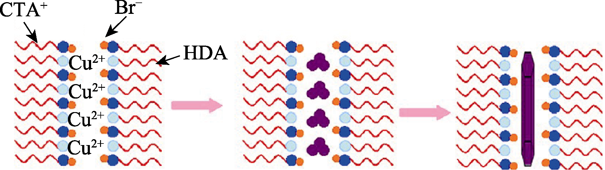
图1 液晶结构介质中铜纳米线形成机制示意图[14]
Fig. 1 Formation of Cu nanowires directed by liquid-crystalline structure of the medium[14]
| Solvent | Reducing agent | Capping agent | Cu precursor | Average diameter/nm | Average length | Ref. |
|---|---|---|---|---|---|---|
| DI water | H3PO3 | Sodium dodecyl benzene sulfonate (SDBS) | CuSO4·5H2O, | ~85 | Tens of micrometers | [17] |
| DI water | Hydrazine hydrate | Ethylenediamine | Cu(NO3)2 | 35-70 | 20-80 μm | [11-13, 18] |
| DI water | Ascorbic Acid | PVP | Cu(NO3)2 | ~50 | >10 μm | [19] |
| DI water | Glucose | HDA | CuCl2·2H2O | 24±4 | Tens to hundreds micrometers | [20] |
| DI water | Glucose | Oleic acid, Oleylamine | CuCl2 | ~45 | 60-90 μm | [9] |
| 1-hexadecylamine (HDA) | 1-Hexadecylamine (HDA) | Hexadecyl trimethyl ammonium bromide (CTAB) | Cu(acac)2 | ~78 | Tens to hundreds micrometers | [14] |
| Oleylamine | Oleylamine | Oleylamine | CuCl | ~63 | 10-30 μm | [10] |
| Oleylamine | Oleylamine | Oleylamine | CuBr2/CuCl2 | 16.2-90.0 | 20-40 μm | [15-16] |
| Oleylamine | Tris(trimethylsilyl) silane | Oleylamine | CuCl2 | ~16.1 | ~17 μm | [21] |
表1 常见铜纳米线合成方法
Table 1 Summary of representitive synthetic methods of Cu nanowires
| Solvent | Reducing agent | Capping agent | Cu precursor | Average diameter/nm | Average length | Ref. |
|---|---|---|---|---|---|---|
| DI water | H3PO3 | Sodium dodecyl benzene sulfonate (SDBS) | CuSO4·5H2O, | ~85 | Tens of micrometers | [17] |
| DI water | Hydrazine hydrate | Ethylenediamine | Cu(NO3)2 | 35-70 | 20-80 μm | [11-13, 18] |
| DI water | Ascorbic Acid | PVP | Cu(NO3)2 | ~50 | >10 μm | [19] |
| DI water | Glucose | HDA | CuCl2·2H2O | 24±4 | Tens to hundreds micrometers | [20] |
| DI water | Glucose | Oleic acid, Oleylamine | CuCl2 | ~45 | 60-90 μm | [9] |
| 1-hexadecylamine (HDA) | 1-Hexadecylamine (HDA) | Hexadecyl trimethyl ammonium bromide (CTAB) | Cu(acac)2 | ~78 | Tens to hundreds micrometers | [14] |
| Oleylamine | Oleylamine | Oleylamine | CuCl | ~63 | 10-30 μm | [10] |
| Oleylamine | Oleylamine | Oleylamine | CuBr2/CuCl2 | 16.2-90.0 | 20-40 μm | [15-16] |
| Oleylamine | Tris(trimethylsilyl) silane | Oleylamine | CuCl2 | ~16.1 | ~17 μm | [21] |
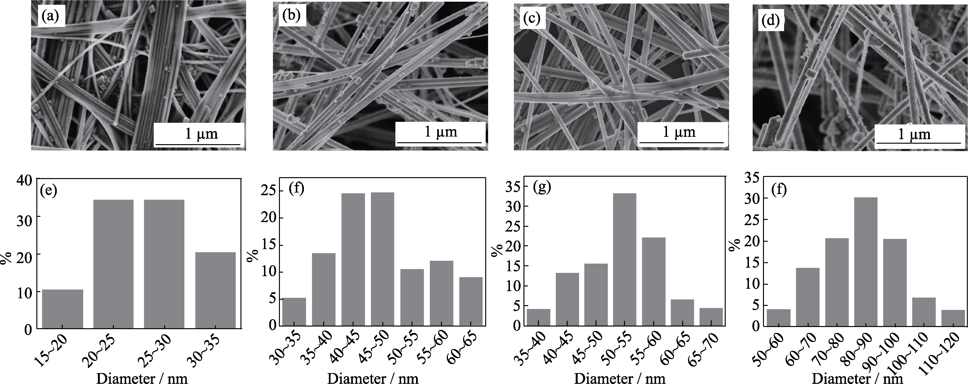
图2 不同合成条件下所得到铜纳米线的微观形貌及直径分布[16]
Fig. 2 SEM images and diameter distribution of Cu nanowires synthesized by using different halide ions[16] (a, e) 2.6 mmol Cl-; (b,f) 2.0 mmol Cl-; (c,g) 1.6 mmol Cl-; (d,h) 1.6 mmol Br-

图3 (A)铜镍双金属纳米线的SEM照片, 插图为纳米线的高分辨SEM照片; (B)铜镍双金属纳米线的暗场光学显微镜照片; (C)~(H)不同Ni含量条件下铜镍双金属纳米线的元素分布[23]
Fig. 3 (A) SEM image of Cu-Ni NWs with inset showing high resolution SEM image of Cu-Ni NWs; (B) Dark field optical microscopy images of Cu-Ni NWs; (C-H) The distribution of Cu and Ni elements of Cu-Ni NWs with different contents of nickel[23]
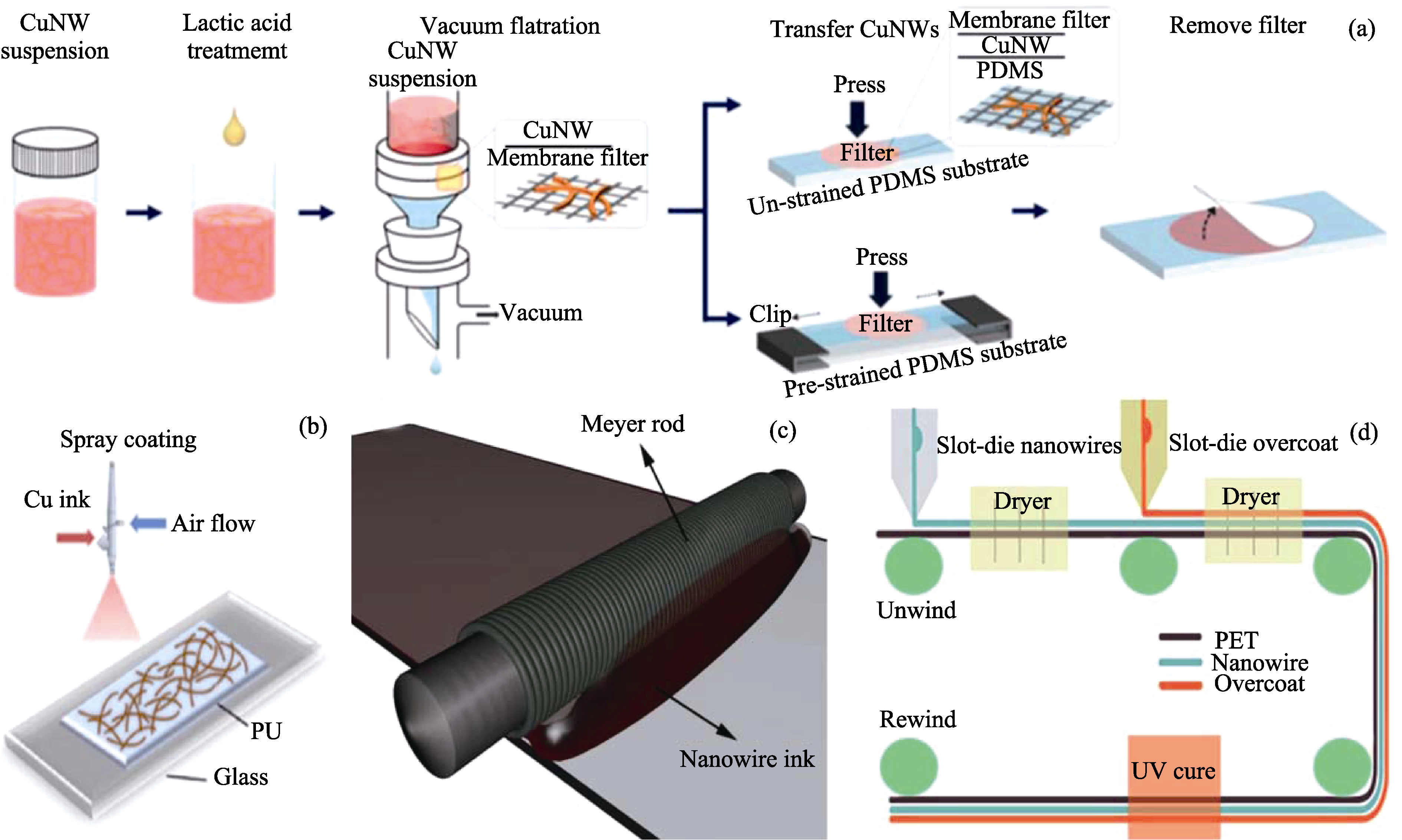
图4 真空抽滤后转移法(a)[35]、喷涂法(b)[36]、梅耶棒涂覆法(c)[37]和卷对卷涂覆法(d)[37]制备纳米线电极示意图
Fig. 4 Schematic diagram of the vaccum transfer method (a)[35], the spray-coating method (b)[36], the meyer rod coating method (c)[37], and the roll-to-roll coating method (d)[37]
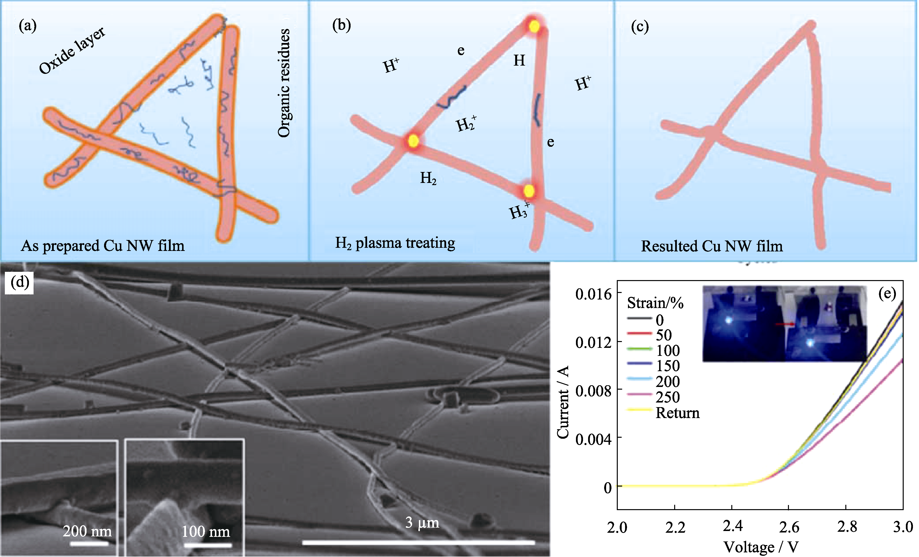
图5 (a)~(c)等离子体后处理方法示意图; (d)经等离子体处理后相邻纳米线搭接点微观形貌; (e)基于等离子体后处理柔性导体的电路在拉伸回复条件下稳定性[48]
Fig. 5 (a-c) Schematic diagram of the experimental setup of a typical plasma treatment process; (d) SEM image of the nanowire junction after plasma treatment; (e) Current-voltage measurement of LED lamps connected by stretchable Cu NW conductors at various strains. Insets are digital photos of the whole setup at 0 and 250% strain[48]
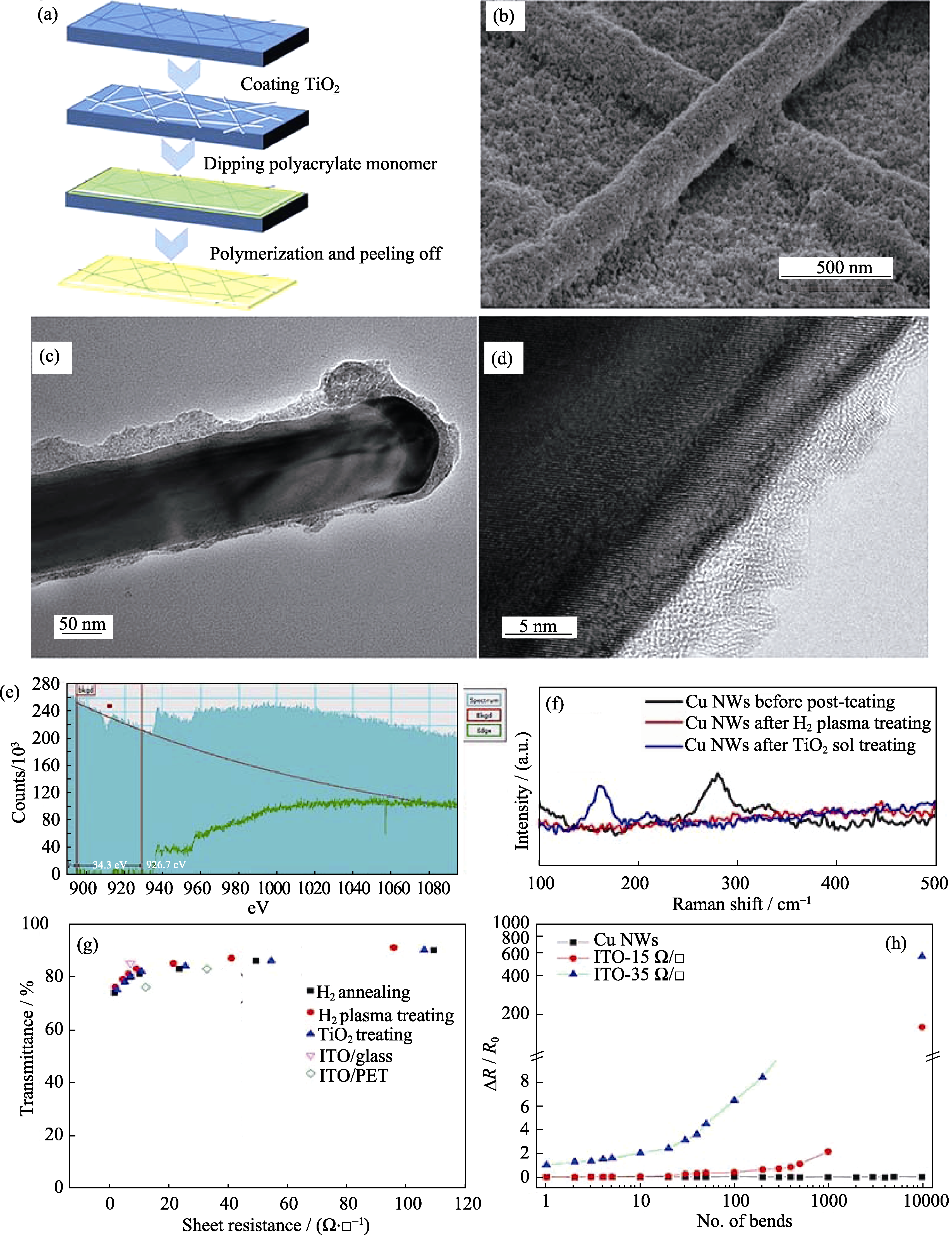
图6 Cu NWs/PA电极的制备流程示意图(a); TiO2处理后的铜纳米线的SEM(b), TEM(c), HRTEM(d)照片和EELS (e)图谱; 处理前、H2 plasma处理以及TiO2处理后的铜纳米线薄膜拉曼图谱(f); H2热处理、H2 plasma 处理以及TiO2处理所得Cu NWs透明导电薄膜的透过率-方阻(g); 通过原位聚合转移后得到的Cu NWs/PA电极和商用的ITO/PET在弯曲104次测试中电阻变化情况(h)[53]
Fig. 6 Schematic diagram (a) of the preparation procedure of Cu NWs/PA electrode. SEM (b), TEM (c), HRTEM (d) and EELS spetra (e) of the Cu NWs film after TiO2 nanopartical sol treatment. Raman spectra (f) of Cu NWs before post-treating, after H2 plasma treatment and TiO2 nanopartical sol treatment. Plot of the transmittance (at a wavelength of 550 nm) with respect to the sheet resistance (g) for films of Cu NWs with H2 annealing, H2 plasma treatment and TiO2 nanopartical sol treatment. Sheet resistance variation (h) of the commercial ITO/PET and Cu NWs/PA electrodes during the bending test of 104 cycles[53]
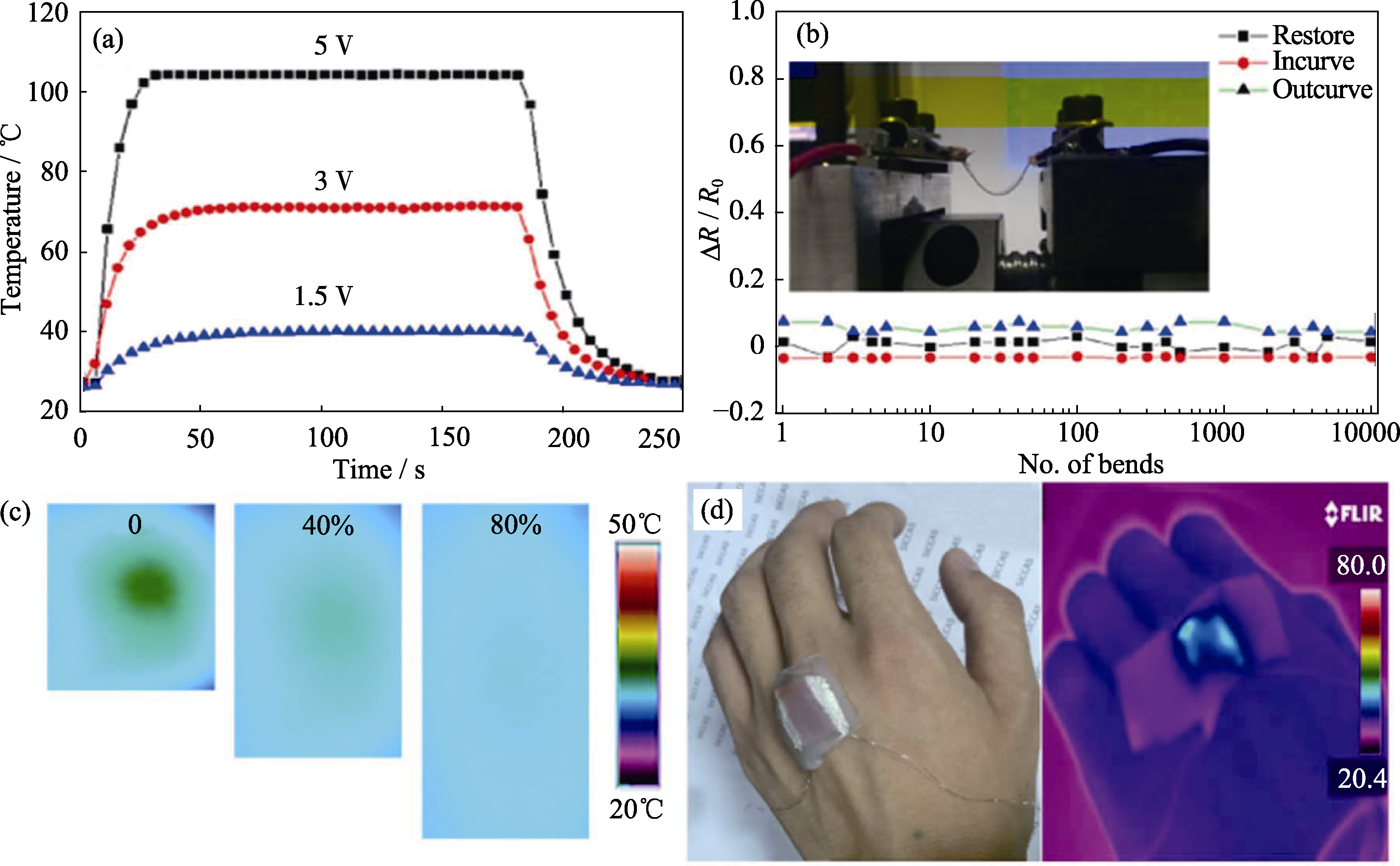
图7 (a) PET衬底上Cu纳米线电极在不同电压条件下温度随时间变化曲线; (b) PET/Cu NW/PMMA电极机械变形下电极电阻稳定性; (c)~(d)铜纳米线基可拉伸电加热元件红外照片及示意图[61]
Fig. 7 (a) Time-dependent temperature curves of Cu NW-1000 on PET films at input voltages of 1.5-5 V under ambient conditions; (b) PET/ITO transparent heaters during 104 cycles of bending tests; (c) Infrared photograph and (d) application examples of Cu NW-based stretchable heater[61]
| [1] | CHENG H Y, LUO J, HUANG L Q, et al.Preparation of flexible dye-sensitized solar cells based on hierarchical structure ZnO nanosheets. Journal of Inorganic Materials, 2018, 33(5): 507-514. |
| [2] | ZHANG J, YANG X, DENG H, et al. Low-dimensional halide perovskites and their advanced optoelectronic applications. Nano-Micro Letters, 2017, 9(3): 36-1-26. |
| [3] | GUERRERO A, GARCIA-BELMONTE G. Recent advances to understand morphology stability of organic photovoltaics. Nano- Micro Letters, 2016, 9(1): 10-1-16. |
| [4] | CHEN D, LÜ J G, HUANG J Y, et al.Performances of GaN-based LEDs with AZO films as transparent electrodes. Journal of Inorganic Materials, 2013, 28(6): 649-652. |
| [5] | HAN S S, LIU L Y, SHAN Y K, et al.Research of graphene/ antireflection nanostructure composite transparent conducting films. Journal of Inorganic Materials, 2017, 32(2): 197-202. |
| [6] | HUANG W, ZHU J Y, LI H, et al.Preparation and characterization of graphene/carbon nanotube hybrid thin films by drop-coating. Journal of Inorganic Materials, 2017, 32(2): 203-209. |
| [7] | LEE J, LEE P, LEE H, et al.Very long Ag nanowire synthesis and its application in a highly transparent, conductive and flexible metal electrode touch panel. Nanoscale, 2012, 4(20): 6408-6414. |
| [8] | HU L B, WU H, CUI Y.Metal nanogrids, nanowires, and nanofibers for transparent electrodes. MRS Bulletin, 2011, 36(10): 760-765. |
| [9] | LI S, CHEN Y, HUANG L, et al.Large-scale synthesis of well-dispersed copper nanowires in an electric pressure cooker and their application in transparent and conductive networks. Inorganic Chemistry, 2014, 53(9): 4440-4444. |
| [10] | YANG H J, HE S Y, TUAN H Y.Self-seeded growth of five-fold twinned copper nanowires: mechanistic study, characterization, and SERS applications. Langmuir, 2014, 30(2): 602-610. |
| [11] | CHANG Y, LYE M L, ZENG H C.Large-scale synthesis of high-quality ultralong copper nanowires. Langmuir, 2005, 21(9): 3746-3748. |
| [12] | YE S, RATHMELL A R, HA Y C, et al.The role of cuprous oxide seeds in the one-pot and seeded syntheses of copper nanowires. Small, 2014, 10(9): 1771-1778. |
| [13] | RATHMELL A R, WILEY B J.The synthesis and coating of long, thin copper nanowires to make flexible, transparent conducting films on plastic substrates. Advanced Materials, 2011, 23(41): 4798-4803. |
| [14] | ZHANG D, WANG R, WEN M, et al.Synthesis of ultralong copper nanowires for high-performance transparent electrodes. Journal of the American Chemical Society, 2012, 134(35): 14283-14286. |
| [15] | GUO H, LIN N, CHEN Y, et al. Copper nanowires as fully transparent conductive electrodes. Scientific Reports, 2013, 3: 2323-1-8. |
| [16] | WANG X, WANG R, SHI L, et al.Kinetically controlled synthesis of Cu nanowires with tunable diameters and their applications in transparent electrodes. Journal of Materials Chemistry C, 2018, 6(5): 1048-1056. |
| [17] | LIU Z, YANG Y, LIANG J, et al.Synthesis of copper nanowires via a complex-surfactant-assisted hydrothermal reduction process. The Journal of Physical Chemistry B, 2003, 107(46): 12658-12661. |
| [18] | YE S, RATHMELL A R, STEWART I E, et al.A rapid synthesis of high aspect ratio copper nanowires for high-performance transparent conducting films. Chemical Communications, 2014, 50(20): 2562-2564. |
| [19] | ZHANG X, ZHANG D, NI X, et al.One-step preparation of copper nanorods with rectangular cross sections. Solid State Communications, 2006, 139(8): 412-414. |
| [20] | JIN M, HE G, ZHANG H, et al.Shape-controlled synthesis of copper nanocrystals in an aqueous solution with glucose as a reducing agent and hexadecylamine as a capping agent. Angewandte Chemie, 2011, 50(45): 10560-10564. |
| [21] | CUI F, YU Y, DOU L, et al.Synthesis of ultrathin copper nanowires using tris(trimethylsilyl)silane for high-performance and low-haze transparent conductors. Nano Letters, 2015, 15(11): 7610-7615. |
| [22] | RATHMELL A R, NGUYEN M, CHI M, et al.Synthesis of oxidation- resistant cupronickel nanowires for transparent conducting nanowire networks. Nano Letters, 2012, 12(6): 3193-3199. |
| [23] | WANG X, WANG R, SHI L, et al.Synthesis of metal/bimetal nanowires and their applications as flexible transparent electrodes. Small, 2015, 11(36): 4737-4744. |
| [24] | SOREL S, LYONS P E, DE S, et al. The dependence of the optoelectrical properties of silver nanowire networks on nanowire length and diameter. Nanotechnology, 2012, 23(18): 185201-1-10. |
| [25] | LAGRANGE M, LANGLEY D P, GIUSTI G, et al.Optimization of silver nanowire-based transparent electrodes: effects of density, size and thermal annealing. Nanoscale, 2015, 7(41): 17410-17423. |
| [26] | KIM A, WON Y, WOO K, et al.All-solution-processed indium- free transparent composite electrodes based on Ag nanowire and metal oxide for thin-film solar cells. Advanced Functional Materials, 2014, 24(17): 2462-2471. |
| [27] | FINN D J, LOTYA M, COLEMAN J N.Inkjet printing of silver nanowire networks. ACS Applied Materials & Interfaces, 2015, 7(17): 9254-9261. |
| [28] | LU H, LIN J, WU N, et al. Inkjet printed silver nanowire network as top electrode for semi-transparent organic photovoltaic devices. Applied Physics Letters, 2015, 106(9): 093302-1-4. |
| [29] | BELLEW A T, BELL A P, MCCARTHY E K, et al.Programmability of nanowire networks. Nanoscale, 2014, 6(16): 9632-9639. |
| [30] | SCARDACI V, COULL R, LYONS P E, et al.Spray deposition of highly transparent, low-resistance networks of silver nanowires over large areas. Small, 2011, 7(18): 2621-2628. |
| [31] | HAUGER T C, AL-RAFIA S M, BURIAK J M. Rolling silver nanowire electrodes: simultaneously addressing adhesion, roughness, and conductivity. ACS Applied Materials & Interfaces, 2013, 5(23): 12663-12671. |
| [32] | BORCHERT J W, STEWART I E, YE S, et al.Effects of length dispersity and film fabrication on the sheet resistance of copper nanowire transparent conductors. Nanoscale, 2015, 7(34): 14496-14504. |
| [33] | KOGA H, NOGI M, KOMODA N, et al. Uniformly connected conductive networks on cellulose nanofiber paper for transparent paper electronics. npg Asia Mater., 2014, 6(3): e93-1-8. |
| [34] | DENG B, HSU P C, CHEN G, et al.Roll-to-roll encapsulation of metal nanowires between graphene and plastic substrate for high-performance flexible transparent electrodes. Nano Letters, 2015, 15(6): 4206-4213. |
| [35] | WON Y, KIM A, YANG W, et al.A highly stretchable, helical copper nanowire conductor exhibiting a stretchability of 700%. npg Asia Mater., 2014, 6(9): e132-e132. |
| [36] | DING S, JIU J, GAO Y, et al.One-step fabrication of stretchable copper nanowire conductors by a fast photonic sintering technique and its application in wearable devices. ACS Applied Materials & Interfaces, 2016, 8(9): 6190-6199. |
| [37] | YE S, RATHMELL A R, CHEN Z, et al.Metal nanowire networks: the next generation of transparent conductors. Advanced Materials, 2014, 26(39): 6670-6687. |
| [38] | WON Y, KIM A, LEE D, et al. Annealing-free fabrication of highly oxidation-resistive copper nanowire composite conductors for photovoltaics. npg Asia Materials, 2014, 6: e105-1-9. |
| [39] | TAO A, KIM F, HESS C, et al.Langmuir-Blodgett silver nanowire monolayers for molecular sensing using surface-enhanced Raman spectroscopy. Nano Letters, 2003, 3(9): 1229-1233. |
| [40] | LIU J W, WANG J L, WANG Z H, et al.Manipulating nanowire assembly for flexible transparent electrodes. Angewandte Chemie, 2014, 53(49): 13477-13482. |
| [41] | KANG S, KIM T, CHO S, et al.Capillary printing of highly aligned silver nanowire transparent electrodes for high-performance optoelectronic devices. Nano Letters, 2015, 15(12): 7933-7942. |
| [42] | JASON N N, SHEN W, CHENG W.Copper nanowires as conductive ink for low-cost draw-on electronics. ACS Applied Materials & Interfaces, 2015, 7(30): 16760-16766. |
| [43] | GARNETT E C, CAI W, CHA J J, et al.Self-limited plasmonic welding of silver nanowire junctions. Nature Materials, 2012, 11(3): 241-249. |
| [44] | BELL A P, FAIRFIELD J A, MCCARTHY E K, et al.Quantitative study of the photothermal properties of metallic nanowire networks. ACS Nano, 2015, 9(5): 5551-5558. |
| [45] | HAN S, HONG S, HAM J, et al.Fast plasmonic laser nanowelding for a Cu-nanowire percolation network for flexible transparent conductors and stretchable electronics. Advanced Materials, 2014, 26(33): 5808-5814. |
| [46] | SONG T B, CHEN Y, CHUNG C H, et al.Nanoscale Joule heating and electromigration enhanced ripening of silver nanowire contacts. ACS Nano, 2014, 8(3): 2804-2811. |
| [47] | MAIZE K, DAS S R, SADEQUE S, et al. Super-Joule heating in graphene and silver nanowire network. Applied Physics Letters, 2015, 106(14): 143104-1-6. |
| [48] | WANG R, ZHAI H, WANG T, et al.Plasma-induced nanowelding of a copper nanowire network and its application in transparent electrodes and stretchable conductors. Nano Research, 2016, 9(7): 2138-2148. |
| [49] | LU H, ZHANG D, REN X, et al.Selective growth and integration of silver nanoparticles on silver nanowires at room conditions for transparent nano-network electrode. ACS Nano, 2014, 8(10): 10980-10987. |
| [50] | LU H F, ZHANG D, CHENG J Q, et al.Locally welded silver nano-network transparent electrodes with high operational stability by a simple alcohol-based chemical approach. Advanced Functional Materials, 2015, 25(27): 4211-4218. |
| [51] | XIONG W, LIU H, CHEN Y, et al.Highly conductive, air-stable silver nanowire@iongel composite films toward flexible transparent electrodes. Advanced Materials, 2016, 28(33): 7167-7172. |
| [52] | WANG X, WANG R, ZHAI H, et al.Room-temperature surface modification of Cu nanowires and their applications in transparent electrodes, SERS-based sensors, and organic solar cells. ACS Applied Materials & Interfaces, 2016, 8(42): 28831-28837. |
| [53] | ZHAI H, LI Y, CHEN L, et al.Copper nanowire-TiO2-polyacrylate composite electrodes with high conductivity and smoothness for flexible polymer solar cells. Nano Research, 2018, 11(4): 1895-1904. |
| [54] | ZHAI H, LI Y, CHEN L, et al.Semi-transparent polymer solar cells with all-copper nanowire electrodes. Nano Research, 2018, 11(4): 1956-1966. |
| [55] | ZHAI H, WANG R, WANG W, et al.Novel fabrication of copper nanowire/cuprous oxidebased semiconductor-liquid junction solar cells. Nano Research, 2015, 8(10): 3205-3215. |
| [56] | HSU P C, LIU X, LIU C, et al.Personal thermal management by metallic nanowire-coated textile. Nano Letters, 2015, 15(1): 365-371. |
| [57] | GUPTA R, RAO K D, KIRUTHIKA S, et al.Visibly transparent heaters. ACS Applied Materials & Interfaces, 2016, 8(20): 12559-12575. |
| [58] | KANG J, KIM H, KIM K S, et al.High-performance graphene- based transparent flexible heaters. Nano Letters, 2011, 11(12): 5154-5158. |
| [59] | JANAS D, KOZIOL K K.A review of production methods of carbon nanotube and graphene thin films for electrothermal applications. Nanoscale, 2014, 6(6): 3037-3045. |
| [60] | CELLE C, MAYOUSSE C, MOREAU E, et al.Highly flexible transparent film heaters based on random networks of silver nanowires. Nano Research, 2012, 5(6): 427-433. |
| [61] | ZHAI H, WANG R, WANG X, et al.Transparent heaters based on highly stable Cu nanowire films. Nano Research, 2016, 9(12): 3924-3936. |
| [62] | IM H G, JUNG S H, JIN J, et al.Flexible transparent conducting hybrid film using a surface-embedded copper nanowire network: a highly oxidation-resistant copper nanowire electrode for flexible optoelectronics. ACS Nano, 2014, 8(10): 10973-10979. |
| [63] | CHENG Y, WANG S, WANG R, et al.Copper nanowire based transparent conductive films with high stability and superior stretchability. Journal of Materials Chemistry C, 2014, 2(27): 5309-5316. |
| [64] | WANG T, WANG R, CHENG Y, et al.Quasi in situ polymerization to fabricate copper nanowire-based stretchable conductor and its applications. ACS Applied Materials & Interfaces, 2016, 8(14): 9297-9304. |
| [65] | CHEN Z, RATHMELL A R, YE S, et al.Optically transparent water oxidation catalysts based on copper nanowires. Angewandte Chemie International Edition, 2013, 52(51): 13708-13711. |
| [66] | XIAO S, LIU P, ZHU W, et al.Copper nanowires: a substitute for noble metals to enhance photocatalytic H2 generation. Nano Letters, 2015, 15(8): 4853-4858. |
| [67] | PARK S G, MUN C, LEE M, et al.3D hybrid plasmonic nanomaterials for highly efficient optical absorbers and sensors. Advanced Materials, 2015, 27(29): 4290-4295. |
| [1] | 陈明俊, 缪洪康, 肖英俊, 邓建波, 张翔, 赵九蓬, 李垚. 光-热双响应材料研究进展: 从设计策略到智能窗应用[J]. 无机材料学报, 2026, 41(6): 723-738. |
| [2] | 宋坤洁, 解荣军. 机器学习驱动新型发光材料的研究进展[J]. 无机材料学报, 2026, 41(6): 689-703. |
| [3] | 胡钰晴, 朱一新, 乐先浩, 万青. 钽酸锂晶圆减薄技术及其热释电红外探测器应用进展[J]. 无机材料学报, 2026, 41(6): 764-774. |
| [4] | 刘春帆, 陈科, 葛芳芳, 黄庆. 核用耐铅铋腐蚀涂层的研究进展[J]. 无机材料学报, 2026, 41(6): 775-786. |
| [5] | 胡扬, 谢敏, 张筱怡, 李想, 郭新伟, 姜南, 周文瀚, 张胜利, 曾海波. 计算与数据驱动环保型发光材料的研究进展[J]. 无机材料学报, 2026, 41(6): 704-722. |
| [6] | 王俊卜, 黄泽皑, 杨茗凯, 蒙颖, 周明炜, 周莹. 甲烷转化用抗积碳催化材料研究进展[J]. 无机材料学报, 2026, 41(6): 739-750. |
| [7] | 王金文, 杨振, 周欢, 夏丹, 杨磊. 可注射无机材料及其生物医学应用[J]. 无机材料学报, 2026, 41(6): 751-763. |
| [8] | 李涵涛, 沈强, 罗国强, 王雪飞, 高明, 陈晨. 机械球磨法调控硅基负极材料结构与性能的研究进展[J]. 无机材料学报, 2026, 41(5): 561-572. |
| [9] | 解陈一, 缪花明, 张蔚然, 刘荣军, 王衍飞, 李端. 理论计算在高熵陶瓷领域的研究进展[J]. 无机材料学报, 2026, 41(5): 545-560. |
| [10] | 李璇, 叶奎材, 冯佳音, 邱家军, 钱文昊, 邢敏. 钛基牙种植体表面改性促进软组织封闭的研究进展[J]. 无机材料学报, 2026, 41(4): 432-444. |
| [11] | 蒋圣楠, 郑重, 何唯一, 刘涛, 潘秀红, 陈锟, 郭辉, 高攀, 刘春俊, 刘学超. 硼镓共掺氧化锌透明电极的制备及性能优化[J]. 无机材料学报, 2026, 41(4): 479-485. |
| [12] | 彭德招, 李瑞, 王文鸿, 王梓瑞, 章志珍. 钠氯化物固态电解质研究进展[J]. 无机材料学报, 2026, 41(4): 409-420. |
| [13] | 陈坤, 姜勇刚, 冯军宗, 李良军, 胡艺洁, 冯坚. 锆酸镧多孔隔热材料研究进展[J]. 无机材料学报, 2026, 41(4): 421-431. |
| [14] | 韦连金, 齐志杰, 汪信, 朱俊武, 付永胜. 纳米金刚石改性及其在电催化氧还原反应中的应用[J]. 无机材料学报, 2026, 41(3): 273-288. |
| [15] | 刘占一, 李勉, 欧阳晓平, 柴之芳, 黄庆. 干法后处理熔盐中Sr/Cs去除方法的研究进展[J]. 无机材料学报, 2026, 41(2): 150-158. |
| 阅读次数 | ||||||
|
全文 |
|
|||||
|
摘要 |
|
|||||