Journal of Inorganic Materials ›› 2024, Vol. 39 ›› Issue (5): 547-553.DOI: 10.15541/jim20230490
Special Issue: 【信息功能】功能晶体(202512)
• RESEARCH ARTICLE • Previous Articles Next Articles
LU Hao1,2( ), XU Shengrui1(), HUANG Yong2, CHEN Xing2, XU Shuang1, LIU Xu1, WANG Xinhao1, GAO Yuan1, ZHANG Yachao1, DUAN Xiaoling1, ZHANG Jincheng1, HAO Yue1
Received:2023-10-20
Revised:2023-11-29
Published:2024-05-20
Online:2024-01-08
Contact:
XU Shengrui, professor. E-mail: srxu@xidian.edu.cnAbout author:LU Hao (1998-), male, Master candidate. E-mail: 2319175454@qq.com
Supported by:CLC Number:
LU Hao, XU Shengrui, HUANG Yong, CHEN Xing, XU Shuang, LIU Xu, WANG Xinhao, GAO Yuan, ZHANG Yachao, DUAN Xiaoling, ZHANG Jincheng, HAO Yue. Epitaxy Single Crystal GaN on AlN Prepared by Plasma-enhanced Atomic Layer Deposition[J]. Journal of Inorganic Materials, 2024, 39(5): 547-553.

Fig. 1 Schematic diagram of plasma-enhanced atomic layer deposition (PEALD) process of AlN

Fig. 2 Cross-sectional TEM image of sample 4

Fig. 3 Surface topographies of AlN AFM 3D images of (a) sample 1, (b) sample 2 and (c) sample 3
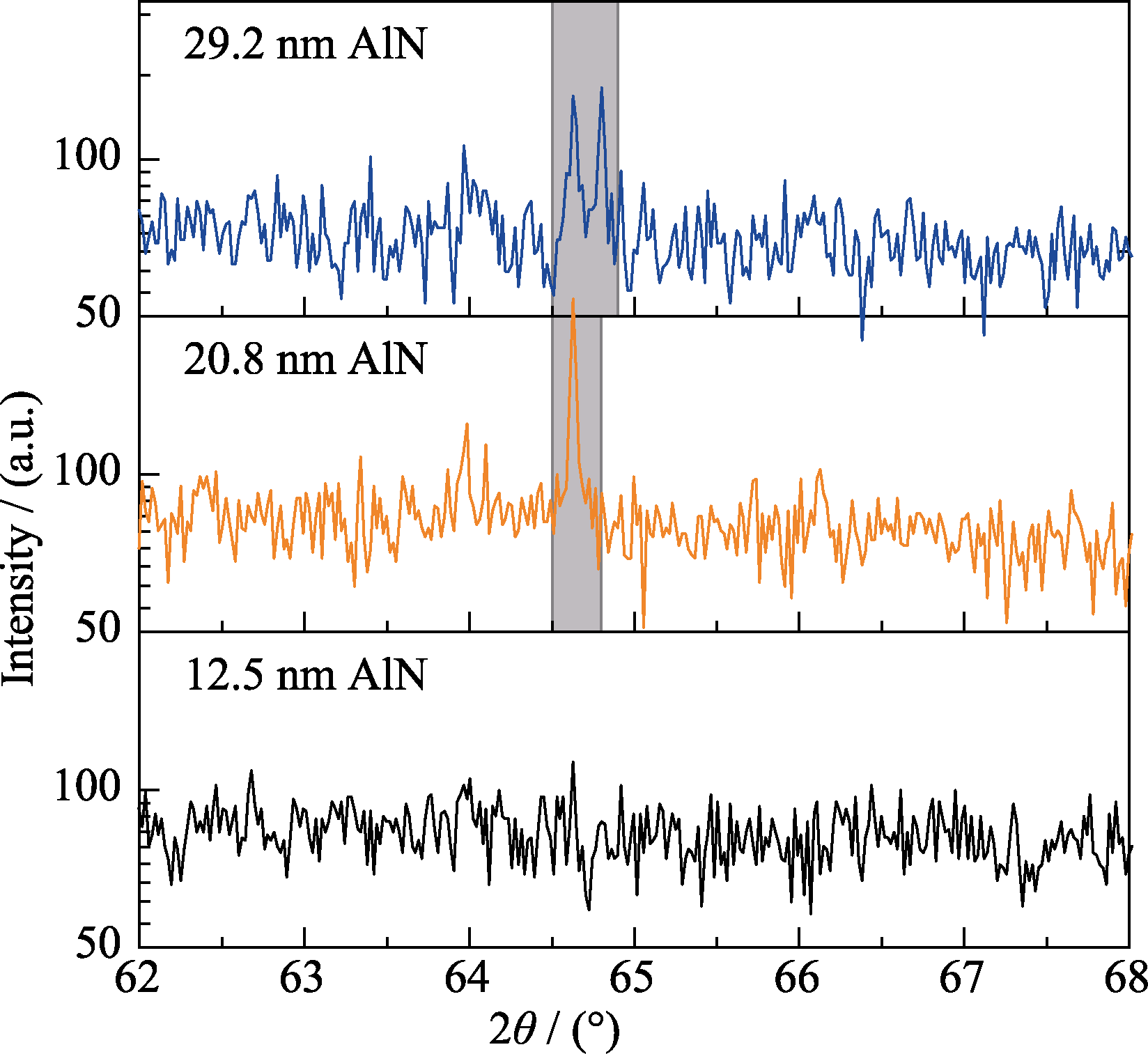
Fig. 4 XRD patterns of AlN films
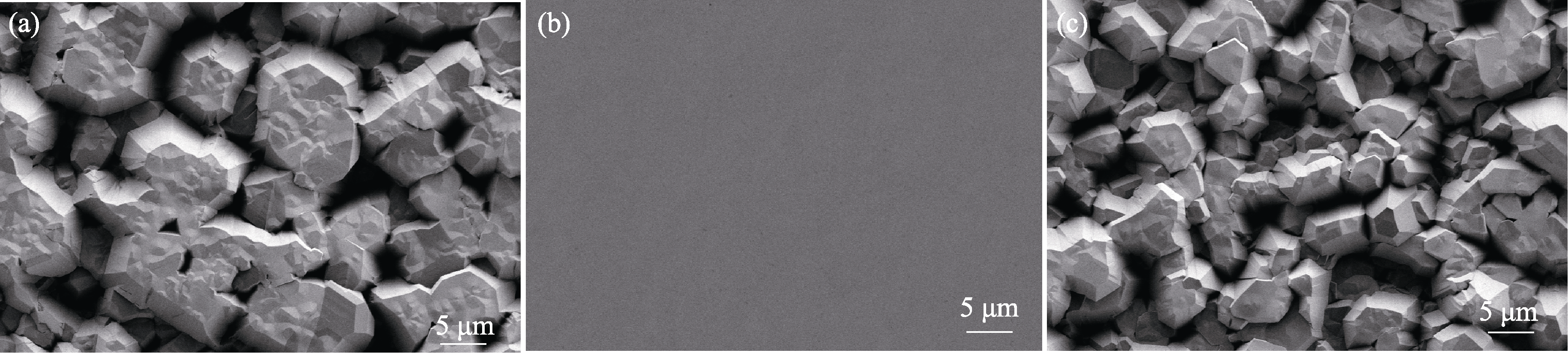
Fig. 5 SEM images of GaN (a) Sample a; (b) Sample b; (c) Sample c
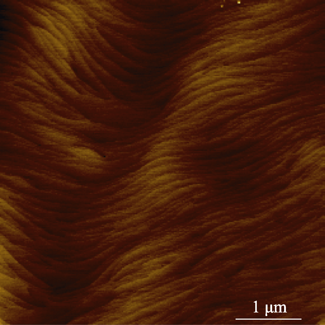
Fig. 6 AFM image of sample b

Fig. 7 Raman spectra of epitaxial GaN on AlN nucleation layers with different thicknesses
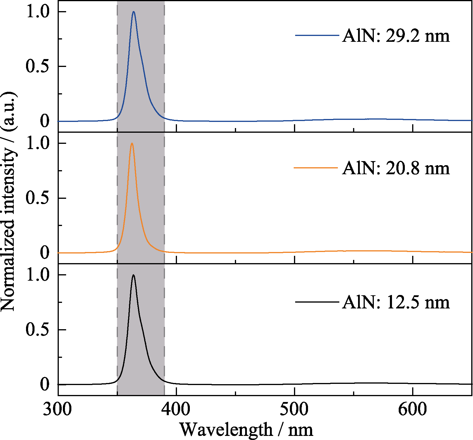
Fig. 8 PL spectra of GaN with different thicknesses of AlN nucleation layers
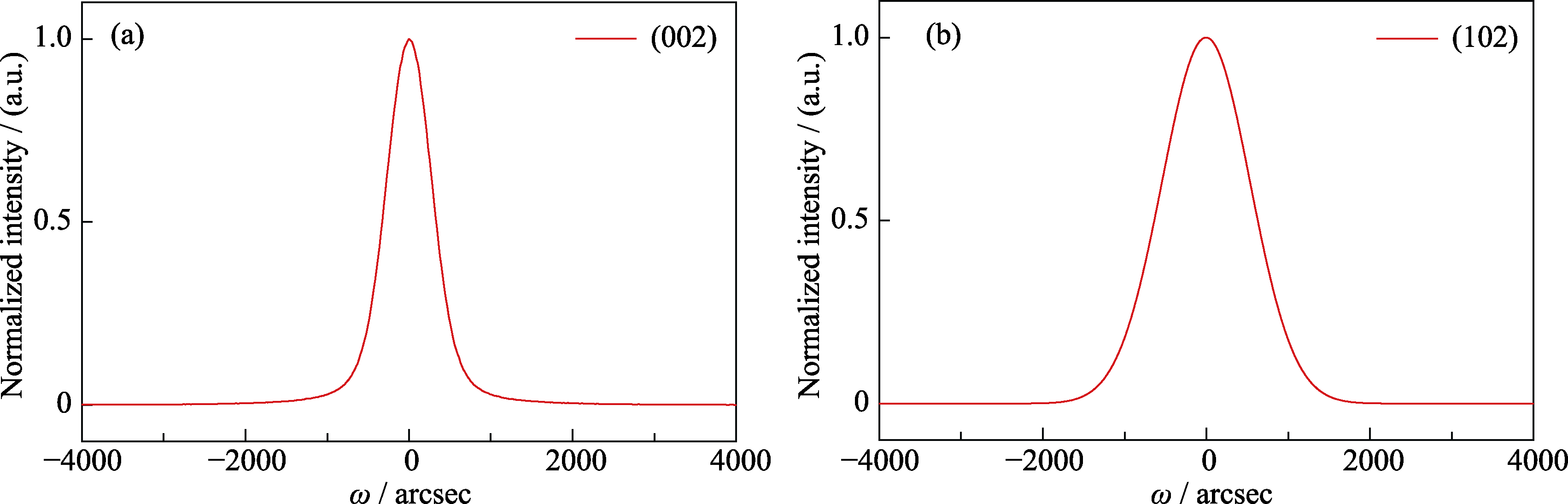
Fig. 9 Rocking curves of sample b on different crystal planes (a) (002); (b) (102)

Fig. 10 Rocking curves of (002) crystal plane for sample a (a) and sample c (b)
| [1] | FOUTZ B E, O’LEARY S K, SHUR M S, et al. Transient electron transport in wurtzite GaN, InN, and AlN. Journal of Applied Physics, 1999, 85(11): 7727. |
| [2] | SHEN L, COFFIE R, BUTTARI D, et al. High-power polarization- engineered GaN/AlGaN/GaN HEMTs without surface passivation. IEEE Electron Device Letters, 2004, 25(1): 7. |
| [3] | AKASAKI I. Key inventions in the history of nitride-based blue LED and LD. Journal of Crystal Growth, 2007, 300(1): 2. |
| [4] |
TAO H C, XU S R, ZHANG J C, et al. Improved crystal quality and enhanced optical performance of GaN enabled by ion implantation induced high-quality nucleation. Optics Express, 2023, 31(13): 20850.
DOI PMID |
| [5] | DU J J, XU S R, PENG R S, et al. Enhancement of optical characteristic of InGaN/GaN multiple quantum-well structures by self-growing air voids. Science China Technological Sciences, 2021, 64(7): 1583. |
| [6] | NAKAMURA S. InGaN multiquantum-well-structure laser diodes with GaN-AlGaN modulation-doped strained-layer superlattices. IEEE Journal of Selected Topics in Quantum Electronics, 1998, 4(3): 483. |
| [7] |
RIGUTTI L, TCHERNYCHEVA M, DE LUNA BUGALLO A, et al. Ultraviolet photodetector based on GaN/AlN quantum disks in a single nanowire. Nano Letters, 2010, 10(8): 2939.
DOI PMID |
| [8] | WANG S S, GU B, XU Y, et al. Growth methods and its applications in optoelectronic devices of GaN-based semiconductor materials. Chinese Journal of Electron Devices, 2002, 25(1): 1. |
| [9] | AMANO H, SAWAKI N, AKASAKI I, et al. Metalorganic vapor phase epitaxial growth of a high quality GaN film using an AlN buffer layer. Applied Physics Letters, 1986, 48(5): 353. |
| [10] | YEN C H, LAI W C, YANG Y Y, et al. GaN-based light-emitting diode with sputtered AlN nucleation layer. IEEE Photonics Technology Letters, 2012, 24(4): 294. |
| [11] | WANG L, WANG L, REN F, et al. GaN grown on AlN/sapphire templates. Acta Physica Sinica, 2010, 59(11): 8021. |
| [12] | ZHANG X Y, PENG D C, HAN J, et al. Effect of substrate temperature on properties of AlN buffer layer grown by remote plasma ALD. Surfaces and Interfaces, 2023, 36: 102589. |
| [13] | FARES C, REN F, TADJER M J, et al. Band offset determination for amorphous Al2O3 deposited on bulk AlN and atomic-layer epitaxial AlN on sapphire. Applied Physics Letters, 2020, 117(18): 182103. |
| [14] | BOSUND M, SAJAVAARA T, LAITINEN M, et al. Properties of AlN grown by plasma enhanced atomic layer deposition. Applied Surface Science, 2011, 257(17): 7827. |
| [15] | SHIH H Y, LEE W H, KAO W C, et al. Low-temperature atomic layer epitaxy of AlN ultrathin films by layer-by-layer, in-situ atomic layer annealing. Science Reports, 2017, 7: 39717. |
| [16] | KOEHLER A D, NEPAL N, ANDERSON T J, et al. Atomic layer epitaxy AlN for enhanced AlGaN/GaN HEMT passivation. IEEE Electron Device Letters, 2013, 34(9): 1115. |
| [17] |
CHEN D, WANG Z, HU F C, et al. Improved electro-optical and photoelectric performance of GaN-based micro-LEDs with an atomic layer deposited AlN passivation layer. Optics Express, 2021, 29(22): 36559.
DOI PMID |
| [18] | LIU C, LIU S, HUANG S, et al. Plasma-enhanced atomic layer deposition of AlN epitaxial thin film for AlN/GaN heterostructure TFTs. IEEE Electron Device Letters, 2013, 34(9): 1106. |
| [19] | NEPAL N, QADRI S B, HITE J K, et al. Epitaxial growth of AlN films via plasma-assisted atomic layer epitaxy. Applied Physics Letters, 2013, 103(8): 082110. |
| [20] | FENG J H, TANG L D, LIU B W, et al. Low-temperature growth of AlN thin films by plasma-enhanced atomic layer deposition. Acta Physica Sinica, 2013, 62(11): 117302. |
| [21] | ELERS K E, RITALA M, LESKELÄ M, et al. Atomic layer epitaxy growth of AIN thin films. Le Journal de Physique IV, 1995, 5(2): 1021. |
| [22] | VAN BUI H, WIGGERS F B, GUPTA A, et al. Initial growth, refractive index, and crystallinity of thermal and plasma-enhanced atomic layer deposition AlN films. Journal of Vacuum Science & Technology A: Vacuum, Surfaces, and Films, 2015, 33(1): 01A111. |
| [23] | HAGEDORN S, KNAUER A, WEYERS M, et al. AlN and AlN/Al2O3 seed layers from atomic layer deposition for epitaxial growth of AlN on sapphire. Journal of Vacuum Science & Technology A: Vacuum, Surfaces, and Films, 2019, 37(2): 020914. |
| [24] | MANASEVIT H M. Single-crystal gallium arsenide on insulating substrates. Applied Physics Letters, 1968, 12(4): 156. |
| [25] | SADEGHPOUR S, CEYSSENS F, PUERS R. Crystalline growth of AlN thin films by atomic layer deposition. Journal of Physics: Conference Series, 2016, 757(1): 012003. |
| [26] | KIM S, OH J, KANG J, et al. Two-step growth of high quality GaN using V/III ratio variation in the initial growth stage. Journal of Crystal Growth, 2004, 262(1/4): 7. |
| [27] | CHEN Z B, ZHANG J C, XU S R, et al. Influence of stacking faults on the quality of GaN films grown on sapphire substrate using a sputtered AlN nucleation layer. Materials Research Bulletin, 2017, 89: 193. |
| [28] | GAO Y, XU S R, PENG R S, et al. Comparative research of GaN growth mechanisms on patterned sapphire substrates with sputtered AlON nucleation layers. Materials, 2020, 13(18): 3933. |
| [29] | MELNIK Y V, VASSILEVSKI K V, NIKITINA I P, et al. Physical properties of bulk GaN crystals grown by HVPE. MRS Internet Journal of Nitride Semiconductor Research, 1997, 2(39): 1. |
| [30] | KOZAWA T, KACHI T, KANO H, et al. Thermal stress in GaN epitaxial layers grown on sapphire substrates. Journal of Applied Physics, 1995, 77(9): 4389. |
| [31] | HUSHUR A, MANGHNANI M H, NARAYAN J. Raman studies of GaN/sapphire thin film heterostructures. Journal of Applied Physics, 2009, 106(5): 054317. |
| [32] | BAN K, YAMAMOTO J I, TAKEDA K, et al. Internal quantum efficiency of whole-composition-range AlGaN multiquantum wells. Applied Physics Express, 2011, 4(5): 052101. |
| [1] | FENG Hengyang, WEI Tianran, QIU Pengfei, SHI Xun. Ultra-large Macroscopic Plastic Deformation and Metalworking in Inorganic Semiconductors [J]. Journal of Inorganic Materials, 2026, 41(6): 681-688. |
| [2] | WANG Jinwen, YANG Zhen, ZHOU Huan, XIA Dan, YANG Lei. Biomedical Applications of Injectable Inorganic Biomaterials [J]. Journal of Inorganic Materials, 2026, 41(6): 751-763. |
| [3] | CHEN Xiaochen, WANG Yang, YANG Bin, WANG Min, A Bohan, WANG Man, ZHANG Lingxia. Ligand-hydroxylated UiO-66 for Enhanced Photothermally Catalytic VOCs Oxidation [J]. Journal of Inorganic Materials, 2026, 41(5): 663-672. |
| [4] | WANG Meng, CAO Leilei, GOU Wangyan, CHENG Yayi, ZHAN Qi, YUAN Menglei. Tandem Catalysis of CuNi Bimetallic MOFs Boosting Nitrate Reduction for Ammonia Production [J]. Journal of Inorganic Materials, 2026, 41(5): 628-636. |
| [5] | WANG Haoyu, KE Xue, GUAN Shiwei, QIAN Shi, LIU Xuanyong. Fe Doped Ti-MOFs for Enhanced Antibacterial Sonodynamic Therapy of Periodontitis [J]. Journal of Inorganic Materials, 2026, 41(4): 527-535. |
| [6] | ZHU Kaihuang, YANG Shijie, LI Xinge, SONG Guanqing, SHI Gansheng, WANG Yan, REN Xiaomeng, LU Yao, XU Xinhong, SUN Jing. Graphene Oxide Modified UiO-66 Based Metal Organic Framework Gel: Preparation and Efficient Toluene Adsorption Performance [J]. Journal of Inorganic Materials, 2026, 41(4): 519-526. |
| [7] | LI Zexi, LU Wenjie, WANG Chao, ZHANG Lu, LI Shuti, GAO Fangliang. Two-dimensional GaN: Preparation Based on Liquid Metal Gallium and Photoelectric Properties [J]. Journal of Inorganic Materials, 2026, 41(3): 377-384. |
| [8] | YAN Gongqin, WANG Chen, LAN Chunbo, HONG Yuxin, YE Weichao, FU Xianghui. Al-doped P2-type Na0.8Ni0.33Mn0.67-xAlxO2 as Cathode for Sodium-ion Batteries: Synthesis and Electrochemical Properties [J]. Journal of Inorganic Materials, 2025, 40(9): 1005-1012. |
| [9] | LIU Jiangping, GUAN Xin, TANG Zhenjie, ZHU Wenjie, LUO Yongming. Research Progress on Catalytic Oxidation of Nitrogen-containing Volatile Organic Compounds [J]. Journal of Inorganic Materials, 2025, 40(9): 933-943. |
| [10] | XIAO Xiaolin, WANG Yuxiang, GU Peiyang, ZHU Zhenrong, SUN Yong. Advances in Regulation of Damaged Skin Regeneration by Two-dimensional Inorganic Materials [J]. Journal of Inorganic Materials, 2025, 40(8): 860-870. |
| [11] | ZHANG Hongjian, ZHAO Ziyi, WU Chengtie. Inorganic Biomaterials on Regulating Neural Cell Function and Innervated Tissue Regeneration: A Review [J]. Journal of Inorganic Materials, 2025, 40(8): 849-859. |
| [12] | MA Wenping, HAN Yahui, WU Chengtie, LÜ Hongxu. Application of Inorganic Bioactive Materials in Organoid Research [J]. Journal of Inorganic Materials, 2025, 40(8): 888-900. |
| [13] | LUO Xiaomin, QIAO Zhilong, LIU Ying, YANG Chen, CHANG Jiang. Inorganic Bioactive Materials Regulating Myocardial Regeneration [J]. Journal of Inorganic Materials, 2025, 40(8): 871-887. |
| [14] | ZHU Wenjie, TANG Lu, LU Jichang, LIU Jiangping, LUO Yongming. Research Progress on Catalytic Oxidation of Volatile Organic Compounds by Perovskite Oxides [J]. Journal of Inorganic Materials, 2025, 40(7): 735-746. |
| [15] | JIANG Zongyu, HUANG Honghua, QING Jiang, WANG Hongning, YAO Chao, CHEN Ruoyu. Aluminum Ion Doped MIL-101(Cr): Preparation and VOCs Adsorption Performance [J]. Journal of Inorganic Materials, 2025, 40(7): 747-753. |
| Viewed | ||||||
|
Full text |
|
|||||
|
Abstract |
|
|||||