Journal of Inorganic Materials ›› 2020, Vol. 35 ›› Issue (10): 1177-1182.DOI: 10.15541/jim20190615
Special Issue: 结构陶瓷论文精选(2020)
• RESEARCH LETTERS • Previous Articles
SUN Futong1,2( ),FENG Aihu2,CHEN Bingbing2,YU Yun2(),YANG Hong1()
Received:2019-12-05
Revised:2020-01-26
Published:2020-10-20
Online:2020-03-06
About author:SUN Futong (1992-), male, Master candidate. E-mail: sunfutong@student.sic.ac.cn。
CLC Number:
SUN Futong, FENG Aihu, CHEN Bingbing, YU Yun, YANG Hong. Effect of Copper Pretreatment on Growth of Graphene Films by Chemical Vapor Deposition[J]. Journal of Inorganic Materials, 2020, 35(10): 1177-1182.
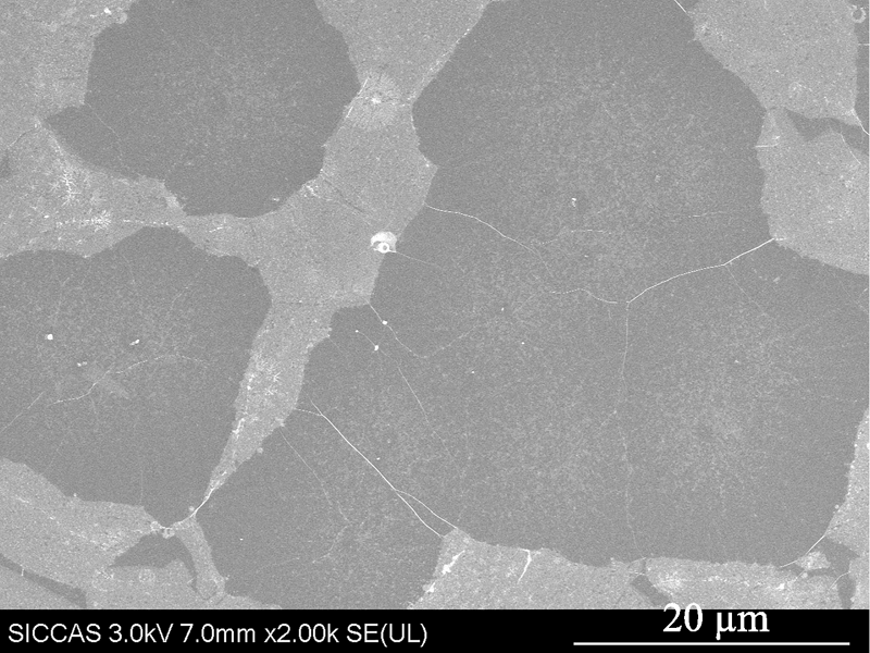
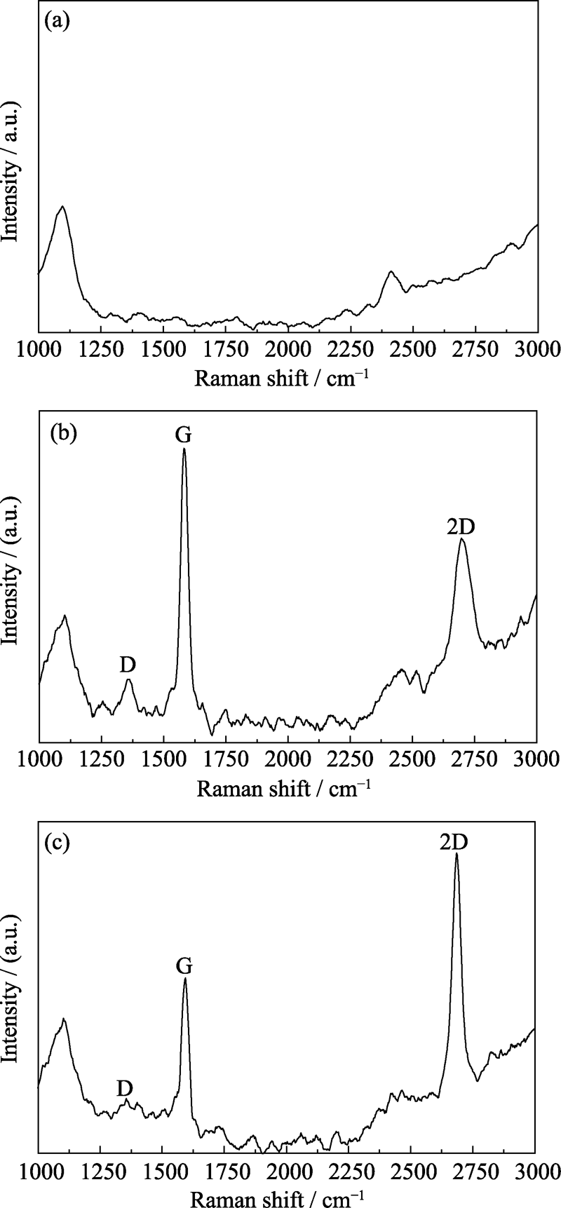
| Area | D band/cm-1 | G band/cm-1 | 2D band/cm-1 | ID/IG | I2D/IG |
|---|---|---|---|---|---|
| Gray area | 1354 | 1581 | 2697 | 0.57 | 0.83 |
| Dark gray area | 1354 | 1592 | 2684 | 0.26 | 1.29 |
| Area | D band/cm-1 | G band/cm-1 | 2D band/cm-1 | ID/IG | I2D/IG |
|---|---|---|---|---|---|
| Gray area | 1354 | 1581 | 2697 | 0.57 | 0.83 |
| Dark gray area | 1354 | 1592 | 2684 | 0.26 | 1.29 |
| [1] |
NOVOSELOV K S, GEIM A K, MOROZOV S V , et al. Electric field effect in atomically thin carbon films. Science, 2004,306(5696):666-669.
DOI URL PMID |
| [2] |
TAN L F, ZENG M Q, WU Q, et al. Direct growth of ultrafast transparent single-layer graphene defoggers. Small, 2015,11(15):1840-1846.
DOI URL PMID |
| [3] |
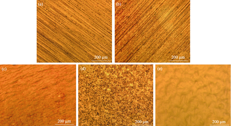
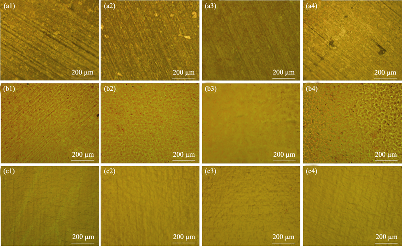
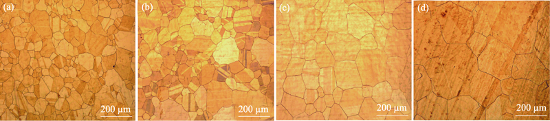
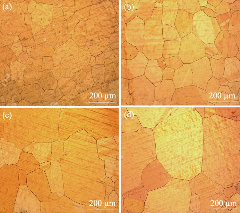
KAPLAS T, KARVONEN L, AHMADI S , et al. Optical characterization of directly deposited graphene on a dielectric substrate. Optics Express, 2016,24(3):2965-2970.
DOI URL PMID |
| [4] |
LI X S, CAI W W, AN J H , et al. Large-area synthesis of high-quality and uniform graphene films on copper foils. Science, 2009,324(5932):1312-1314.
DOI URL PMID |
| [5] | GALASHEV A E . Computer simulation of the thermal stability of nickel films on two-layer graphene. High Temperature, 2014,52(5):633-639. |
| [6] | ZENG J, JI X X, MA Y H , et al. 3D graphene fibers grown by thermal chemical vapor deposition. Advanced Materials, 2018,30(12):1705380. |
| [7] | LIM G, KIHM K D, KIM H G , et al. Enhanced thermoelectric conversion efficiency of cvd graphene with reduced grain sizes. Nanomaterials, 2018,8(7):557. |
| [8] |
XIONG Z, WANG X Y, LEE K H K, et al. Thermal transport in supported graphene nanomesh. ACS Applied Materials & Interfaces, 2018,10(11):9211-9215.
DOI URL PMID |
| [9] |
BALANDIN A A, GHOSH S, BAO W , et al. Superior thermal conductivity of single-layer graphene. Nano Lett, 2008,8(3):902-907.
DOI URL PMID |
| [10] |
REINA A, JIA X, HO J , et al. Large area, few-layer graphene films on arbitrary substrates by chemical vapor deposition. Nano Lett, 2008,9(1):30-35.
DOI URL PMID |
| [11] | ZHANG N, ZHAO X K, FU X B , et al. Preparation and characterization of polyamide-6/reduced graphene oxide composite microspheres. ChemistrySelect, 2019,4(38):11294-11301. |
| [12] | MAHAMAI N, PROM-ANAN T, SARAKONSRI T . Preparation and characterization of platinum alloy catalysts supported on n-doped reduced graphene oxide for anode in direct ethanol fuel cell (DEFC). Materials Today-Proceedings, 2019,17(4):1561-1568. |
| [13] | TIAN J, GUO L, YIN X L , et al. The liquid-phase preparation of graphene by shear exfoliation with graphite oxide as a dispersant. Materials Chemistry and Physics, 2019,223:1-8. |
| [14] | ZHANG D D, FU L, LIAO L , et al. Preparation, characterization, and application of electrochemically functional graphene nanocomposites by one-step liquid-phase exfoliation of natural flake graphite with methylene blue. Nano Research, 2012,5(12):875-887. |
| [15] | MA T, ARIGA H, TAKAKUSAGI S , et al. Smooth epitaxial copper film on sapphire surface suitable for high quality graphene growth. Thin Solid Films, 2018,646:12-16. |
| [16] | MATTEVI C, KIM H, CHHOWALLA M . A review of chemical vapour deposition of graphene on copper. Journal of Materials Chemistry, 2011,21(10):3324-3334. |
| [17] | FANG L P, YUAN W, WANG B , et al. Growth of graphene on Cu foils by microwave plasma chemical vapor deposition: the effect of in-situ hydrogen plasma post-treatment. Applied Surface Science, 2016,383:28-32. |
| [18] | MENDOZA C D, CALDAS P G, FREIRE F L , et al. Growth of single-layer graphene on Ge (100) by chemical vapor deposition. Applied Surface Science, 2018,447:816-821. |
| [19] | WANG H, WANG G Z, BAO P F , et al. Controllable synthesis of submillimeter single-crystal monolayer graphene domains on copper foils by suppressing nucleation. Journal of the American Chemical Society, 2012,134(44):18476-18476. |
| [20] | ZHAO X, GOU L . Comparative analysis of graphene grown on copper and nickel sheet by microwave plasma chemical vapor deposition. Vacuum, 2018,153:48-52. |
| [21] |
GOLI P, NING H, LI X S , et al. Thermal properties of graphene- copper-graphene heterogeneous films. Nano Letters, 2014,14(3):1497-1503.
DOI URL PMID |
| [22] | XU Z . Heat transport in low-dimensional materials: a review and perspective. Theoretical and Applied Mechanics Letters, 2016,6(3):113-121. |
| [23] | YARIFARD M, DAVOODI J, RAFII-TABAR H . Computation of the thermal resistance in graphene sheets with a rectangular hole. Computational Materials Science, 2017,126:29-34. |
| [24] |
LEE W, KIHM K D, KIM H G , et al. In-plane thermal conductivity of polycrystalline chemical vapor deposition graphene with controlled grain sizes. Nano Letters, 2017,17(4):2361-2366.
DOI URL PMID |
| [25] |
THIELE S, REINA A, HEALEY P , et al. Engineering polycrystalline Ni films to improve thickness uniformity of the chemical- vapor-deposition-grown graphene films. Nanotechnology, 2010,21(1):015601.
DOI URL PMID |
| [26] |
HU Y, XIE X, SUN C , et al. Assembling reduced graphene oxide hydrogel with controlled porous structures using cationic and anionic surfactants. Nanotechnology, 2019,30(50):505602.
DOI URL PMID |
| [27] |
KIM S M, HSU A, LEE Y H , et al. The effect of copper precleaning on graphene synthesis. Nanotechnology, 2013,24(36):365602.
URL PMID |
| [28] | HU X D, ZHANG M, XUE Z Y , et al. The effect of copper pretreatment on graphene synthesis by ion implantation into Ni/Cu substrate. Semiconductor Science and Technology, 2018,33(7):074001. |
| [29] |
JEONG H, HWANG W T, SONG Y , et al. Highly uniform monolayer graphene synthesis via a facile pretreatment of copper catalyst substrates using an ammonium persulfate solution. RSC Advances, 2019,9(36):20871-20878.
DOI URL PMID |
|
LI F, LU L Y, GAO D , et al. Rapid synthesis of three-dimensional sulfur-doped porous graphene via solid-state microwave irradiation for protein removal in plasma sample pretreatment. Talanta, 2018,185:528-536.
DOI URL PMID |
| [1] | SUN Li, XU Yongshan, GAO Yihua. Photonic-detection and Bionic-synapse of Graphene/Bi2O2Se/Graphene Bi-heterojunction Device [J]. Journal of Inorganic Materials, 2026, 41(6): 795-804. |
| [2] | WANG Jiahui, LIU Jingjing, QIU Yi, WANG Yongxia, CUI Xiangzhi. Bifunctional Oxygen Electrocatalytic Performance of Atomically Dispersed Fe Anchored on N-doped Graphene [J]. Journal of Inorganic Materials, 2026, 41(6): 814-822. |
| [3] | QIN Ying, YAO Zhuo, ZHENG Lijun, BAO Shuo, LI Peng, GUO Shiqi. Sulfur-doped Graphene/Conductive Polymer Composites: Preparation and Performance as Electrode of Flexible Supercapacitor [J]. Journal of Inorganic Materials, 2026, 41(5): 604-610. |
| [4] | CHENG Aopeng, WANG Yuewen, XU Wentao, LIU Quanwei, ZHANG Haitao, ZHOU Youfu. Fabrication of Graphene-reinforced Alumina Ceramic Composites via Adsorption-precipitation Self-assembly Combined with Spark Plasma Sintering [J]. Journal of Inorganic Materials, 2026, 41(4): 536-544. |
| [5] | ZHU Kaihuang, YANG Shijie, LI Xinge, SONG Guanqing, SHI Gansheng, WANG Yan, REN Xiaomeng, LU Yao, XU Xinhong, SUN Jing. Graphene Oxide Modified UiO-66 Based Metal Organic Framework Gel: Preparation and Efficient Toluene Adsorption Performance [J]. Journal of Inorganic Materials, 2026, 41(4): 519-526. |
| [6] | FAN Yuzhu, WANG Yuan, WANG Linyan, XIANG Meiling, YAN Yuting, LI Benhui, LI Min, WEN Zhidong, WANG Haichao, CHEN Yongfu, QIU Huidong, ZHAO Bo, ZHOU Chengyu. Graphene Oxide-based Adsorbents for Pb(II) Removing in Water: Progresses on Synthesis, Performance and Mechanism [J]. Journal of Inorganic Materials, 2026, 41(1): 12-26. |
| [7] | YANG Mingkai, HUANG Zeai, ZHOU Yunxiao, LIU Tong, ZHANG Kuikui, TAN Hao, LIU Mengying, ZHAN Junjie, CHEN Guoxing, ZHOU Ying. Co-production of Few-layer Graphene and Hydrogen from Methane Pyrolysis Based on Cu and Metal Oxide-KCl Molten Medium [J]. Journal of Inorganic Materials, 2025, 40(5): 473-480. |
| [8] | GAO Chenguang, SUN Xiaoliang, CHEN Jun, LI Daxin, CHEN Qingqing, JIA Dechang, ZHOU Yu. SiBCN-rGO Ceramic Fibers Based on Wet Spinning Technology: Microstructure, Mechanical and Microwave-absorbing Properties [J]. Journal of Inorganic Materials, 2025, 40(3): 290-296. |
| [9] | WANG Yue, WANG Xin, YU Xianli. Room-temperature Ferromagnetic All-carbon Films Based on Reduced Graphene Oxide [J]. Journal of Inorganic Materials, 2025, 40(3): 305-313. |
| [10] | LI Honglan, ZHANG Junmiao, SONG Erhong, YANG Xinglin. Mo/S Co-doped Graphene for Ammonia Synthesis: a Density Functional Theory Study [J]. Journal of Inorganic Materials, 2024, 39(5): 561-568. |
| [11] | SUN Chuan, HE Pengfei, HU Zhenfeng, WANG Rong, XING Yue, ZHANG Zhibin, LI Jinglong, WAN Chunlei, LIANG Xiubing. SiC-based Ceramic Materials Incorporating GNPs Array: Preparation and Mechanical Characterization [J]. Journal of Inorganic Materials, 2024, 39(3): 267-273. |
| [12] | BAO Ke, LI Xijun. Chemical Vapor Deposition of Vanadium Dioxide for Thermochromic Smart Window Applications [J]. Journal of Inorganic Materials, 2024, 39(3): 233-258. |
| [13] | WANG Yanli, QIAN Xinyi, SHEN Chunyin, ZHAN Liang. Graphene Based Mesoporous Manganese-Cerium Oxides Catalysts: Preparation and Low-temperature Catalytic Reduction of NO [J]. Journal of Inorganic Materials, 2024, 39(1): 81-89. |
| [14] | YANG Pingjun, LI Tiehu, LI Hao, DANG Alei. Effect of Graphene on Graphitization, Electrical and Mechanical Properties of Epoxy Resin Carbon Foam [J]. Journal of Inorganic Materials, 2024, 39(1): 107-112. |
| [15] | DONG Yiman, TAN Zhan’ao. Research Progress of Recombination Layers in Two-terminal Tandem Solar Cells Based on Wide Bandgap Perovskite [J]. Journal of Inorganic Materials, 2023, 38(9): 1031-1043. |
| Viewed | ||||||
|
Full text |
|
|||||
|
Abstract |
|
|||||