Journal of Inorganic Materials ›› 2018, Vol. 33 ›› Issue (11): 1225-1231.DOI: 10.15541/jim20180045
• Orginal Article • Previous Articles Next Articles
ZHANG Cong, KANG Chao-Yang, ZONG Hai-Tao, LI Ming, LIANG Shan-Shan, CAO Guo-Hua
Received:2018-01-29
Revised:2018-05-29
Published:2018-11-16
Online:2018-10-20
About author:ZHANG Cong. E-mail: 18839187763@163.com
Supported by:CLC Number:
ZHANG Cong, KANG Chao-Yang, ZONG Hai-Tao, LI Ming, LIANG Shan-Shan, CAO Guo-Hua. Stress Induced Modulation of the Structure and Photoelectric Property of Vanadium Oxide Films on Sapphire Substrate[J]. Journal of Inorganic Materials, 2018, 33(11): 1225-1231.
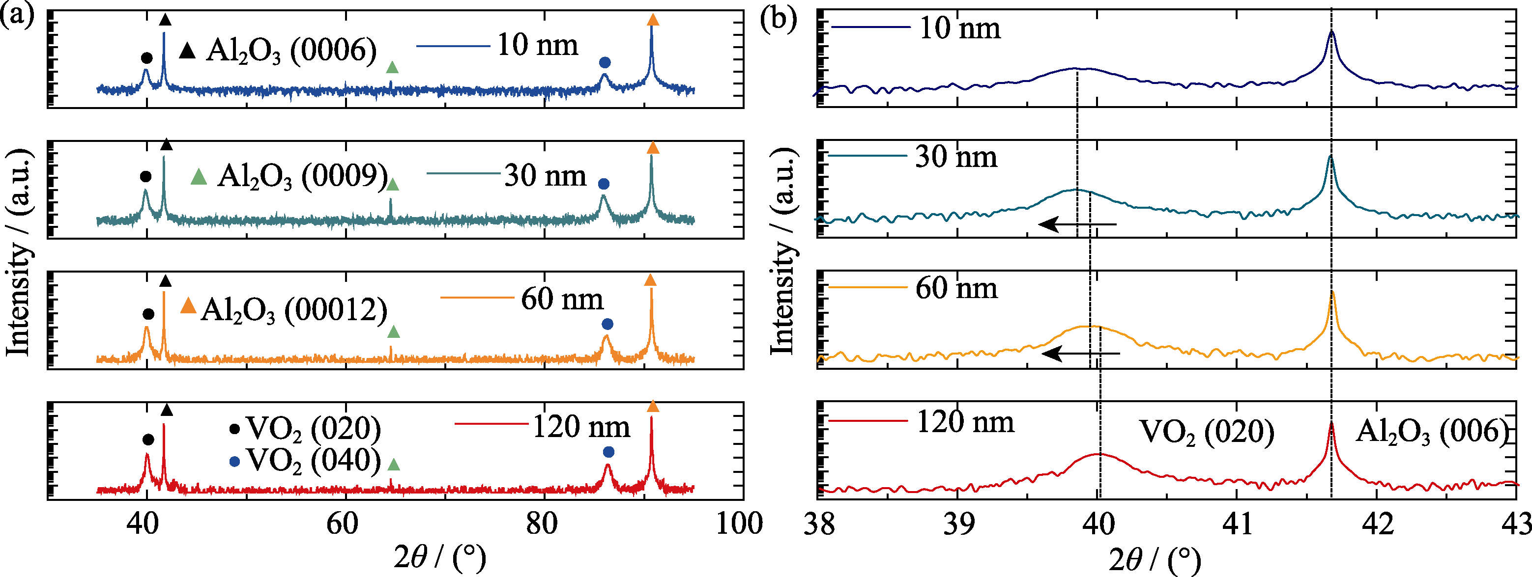
Fig. 1 (a) XRD patterns and (b) amplified XRD patterns in the range of 38°-43° of the VO2 films with different thicknesses deposited on sapphire substrates
| Thickness /nm | VO2 (020) peaks position/(°) | Film stress /MPa | Grain size /nm |
|---|---|---|---|
| 10 | 39.75 | 402 | 13.42 |
| 30 | 39.79 | 67 | 14.90 |
| 60 | 39.98 | -144 | 16.27 |
| 120 | 40.02 | -161 | 21.15 |
Table 1 VO2 (020) peaks position, film strain and the grain sizes of the VO2 films with different thicknesses deposited on sapphire substrates
| Thickness /nm | VO2 (020) peaks position/(°) | Film stress /MPa | Grain size /nm |
|---|---|---|---|
| 10 | 39.75 | 402 | 13.42 |
| 30 | 39.79 | 67 | 14.90 |
| 60 | 39.98 | -144 | 16.27 |
| 120 | 40.02 | -161 | 21.15 |
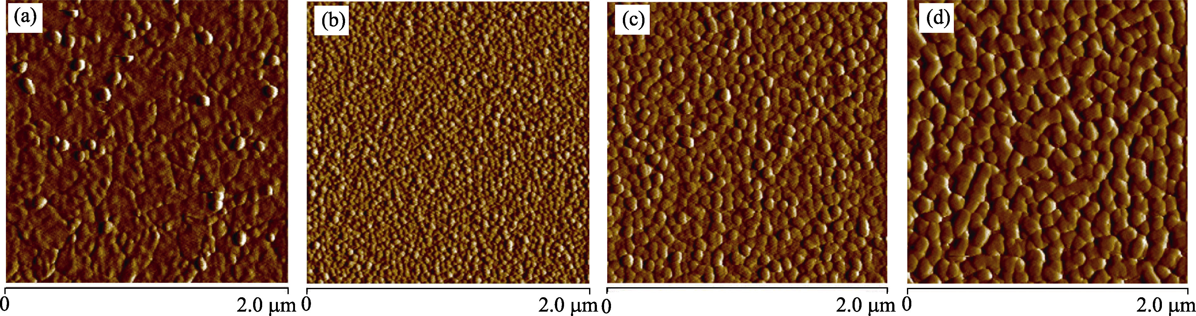
Fig. 2 AFM morphologies of VO2 films with different thicknesses deposited on sapphire substrates ^(a) 10 nm; (b) 30 nm; (c) 60 nm; (d) 120 nm
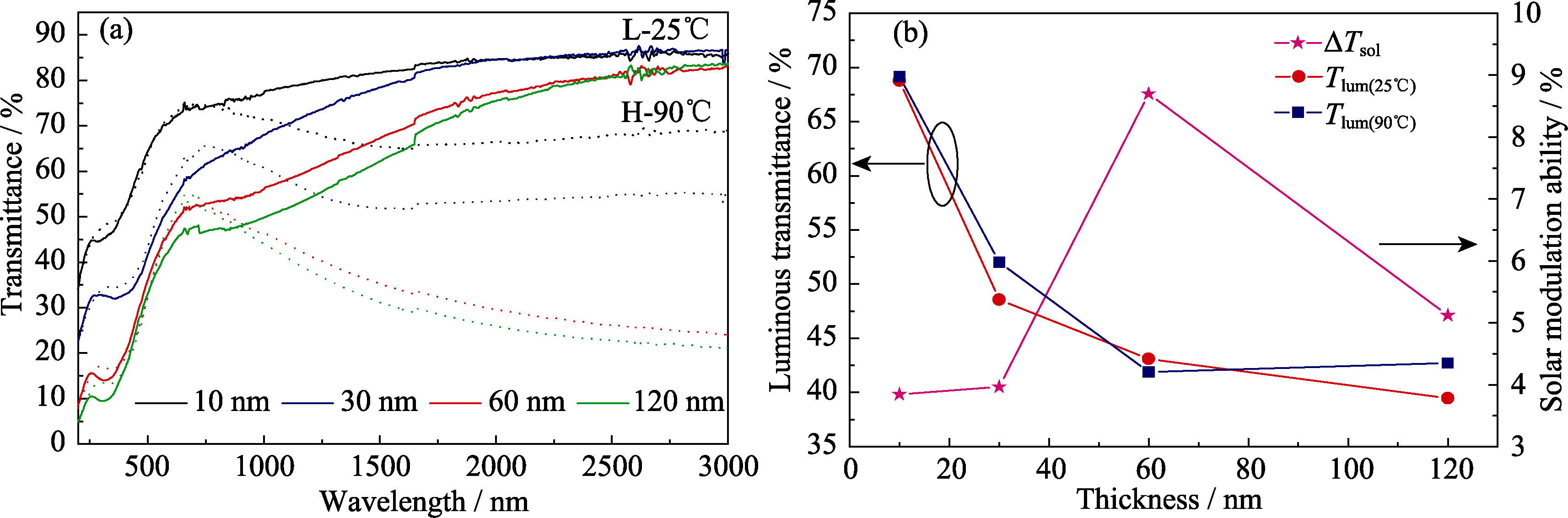
Fig. 3 (a) Transmittance spectra at 25℃ and 90℃ for VO2 films with different thicknesses deposited on sapphire substrates and (b) corresponding variation curves of Tlum(25℃), Tlum(90℃) and ∆Tsol with thickness

Fig. 4 Thermal hysteresis loops of optical transmittance at 2500 nm for VO2 films with different thicknesses deposited on sapphire substrates, with insets showing the corresponding differential curves
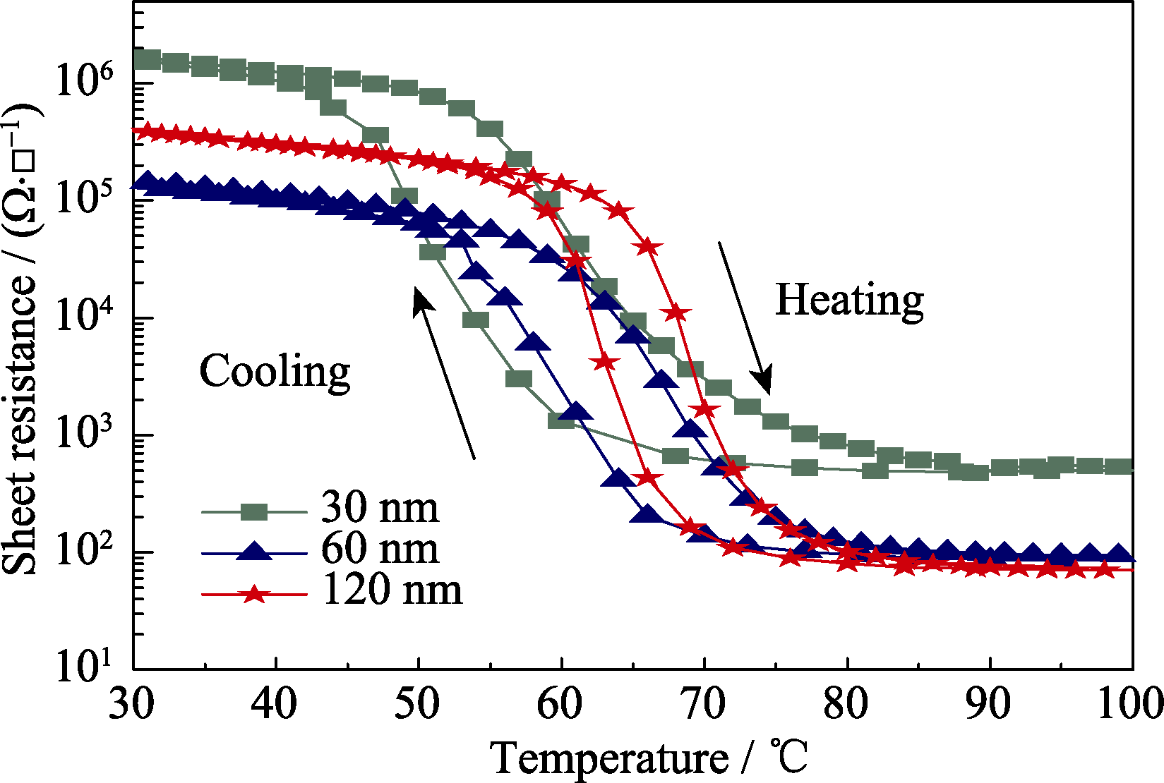
Fig. 5 Thermal hysteresis loops of sheet resistance for VO2 films with different thicknesses deposited on sapphire substrates
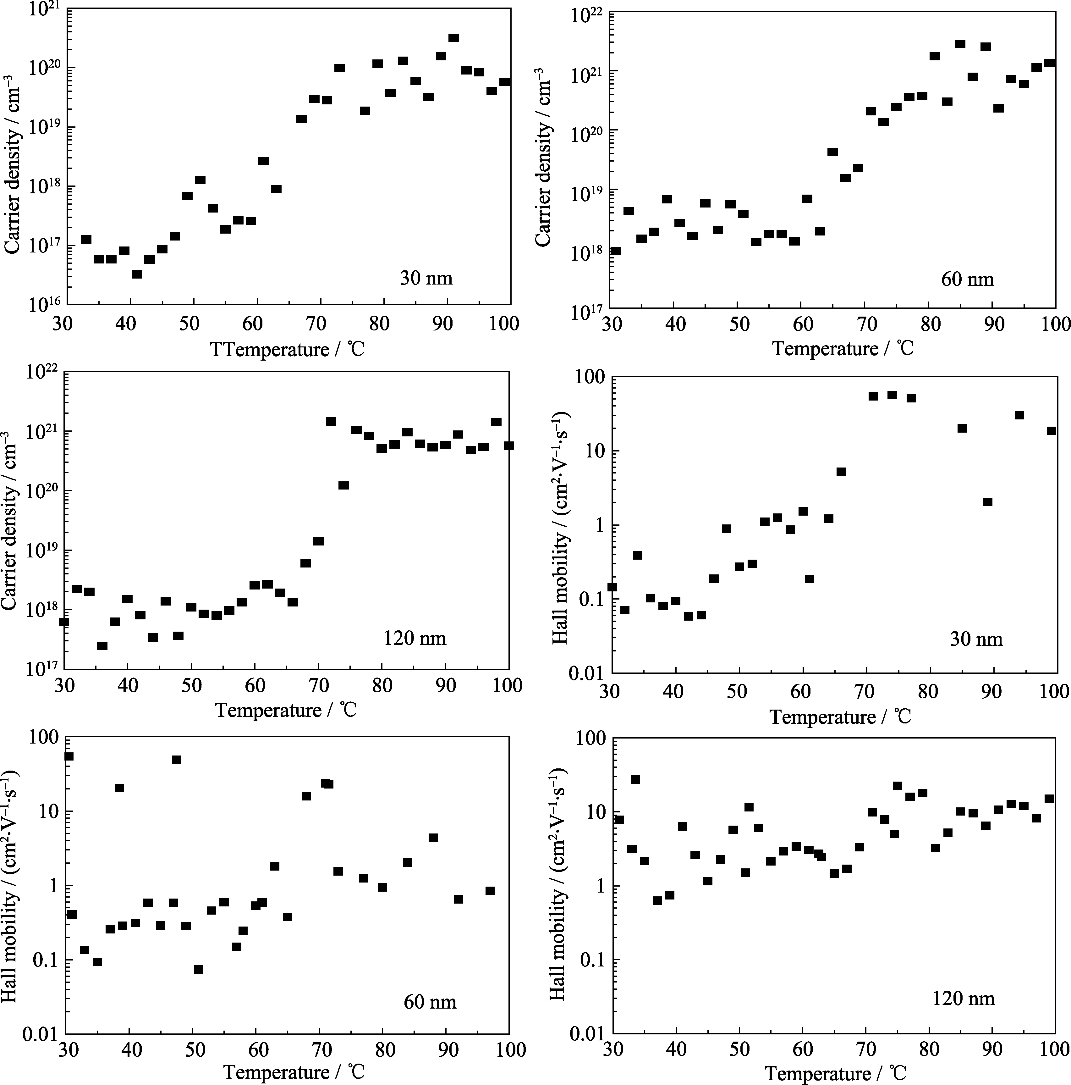
Fig. 6 Temperature dependent carrier density and mobility curves of VO2 films with different thicknesses deposited on sapphire substrates
| [1] | MORIN F J.Oxides which show a metal-to-insulator transition at the neel temperature.Phys. Rev. Lett., 1959, 3(1): 34-36. |
| [2] | GOODENOUGH J B.The two components of the crystallographic transition in VO2.J. Solid State Chem., 1971, 3(4): 490-500. |
| [3] | SUN H J, WANG M H, BIAN J M, et al.Terahertz and metal-insulator transition properties of VO2 film grown on sapphire substrate with MBE.J. Inorg. Mater., 2017, 32(4): 437-442. |
| [4] | GAO Y F, LUO H J, ZHANG Z T, et al.Nanoceramic VO2 thermochromic smart glass: a review on progress in solution processing.Nano Energy, 2012, 1(2): 221-246. |
| [5] | HU B, DING Y, CHEN W, et al.External-strain induced insulating phase rransition in VO2 nanobeam and its application as flexible strain sensor.Adv. Mater., 2010, 22(45): 5134-5139. |
| [6] | ALIEV V S, BORTNIKOV S G,BADMAEVA I A. Anomalous large electrical capacitance of planar microstructures with vanadium dioxide films near the insulator-metal phase transition. Appl. Phys. Lett., 2014, 104(13): 132906-1-4. |
| [7] | LI W J, JI S D, QIAN K, et al.Preparation and characterization of VO2-BaSO4 composite films with enhanced optical properties in thermochromic field.Ceram. Int., 2015, 41(3): 5049-5056. |
| [8] | ZHANG Y F, ZHANG J C, ZHANG X Z, et al.Influence of different additives on the synthesis of VO2 polymorphs.Ceram. Int., 2013, 39(7): 8363-8376. |
| [9] | NAG J, HAGLUND R F.Synthesis of vanadium dioxide thin films and nanoparticles.J. Phys. Condens. Matter, 2008, 20(26): 264016-1-14. |
| [10] | TAKAMI H, KANKI T, UEDA S, et al. Filling-controlled Mott transition in W-doped VO2. Phys. Rev. B, 2012, 85(20): 205111-1-4 . |
| [11] | MLYUKA N R, NIKLASSON G A, GRANQVIST C G. Mg doping of thermochromic VO2 films enhances the optical transmittance and decreases the metal-insulator transition temperature. Appl. Phys. Lett., 2009, 95(17): 171909-1-3. |
| [12] | SHEN N, CHEN S, CHEN Z, et al.The synthesis and performance of Zr-doped and W-Zr-codoped VO2 nanoparticles and derived flexible foils.J. Mater. Chem. A, 2014, 2(36): 15087-15093. |
| [13] | GRANQVIST C G.Transparent conductors as solar energy materials: a panoramic review.Sol. Energ. Mat. Sol. C, 2007, 91(17): 1529-1598. |
| [14] | ZHANG S X, CHOU J Y, LAUHON L J.Direct correlation of structural domain formation with the metal insulator transition in a VO2 nanobeam.Nano Lett., 2009, 9(12): 4527-4532. |
| [15] | LAZAROVITS B, KIM K, HAULE K, et al. Effects of strain on the electronic structure of VO2. Phys. Rev. B, 2010, 81(11): 115117-1-9. |
| [16] | MURAOKA Y, HIROI Z.Metal-insulator transition of VO2 thin films grown on TiO2 (001) and (110) substrates.Appl. Phys. Lett., 2002, 80(4): 583-585. |
| [17] | HU K, YANG Y J, HONG B, et al.Thickness-dependent anisotropy of metal-insulator transition in (110)-VO2/TiO2 epitaxial thin films.J. Alloys Compd., 2017, 699: 575-580. |
| [18] | MARTENS K, AETUKURI N, JEONG J, et al. Improved metal-insulator-transition characteristics of ultrathin VO2 epitaxial films by optimized surface preparation of rutile TiO2 substrates. Appl. Phys. Lett., 2014, 104(8): 081918-1-4. |
| [19] | AETUKURI N B, GRAY A X, DROUARD M, et al.Control of the metal-insulator transition in vanadium dioxide by modifying orbital occupancy.Nat. Phys., 2013, 9(10): 661-666. |
| [20] | FAN L L, CHEN S, LUO Z L, et al.Strain dynamics of ultrathin VO2 film grown on TiO2 (001) and the associated phase transition modulation.Nano Lett., 2014, 14(7): 4036-4043. |
| [21] | YANG T H, AGGARWAL R, GUPTA A, et al. Semiconductor- metal transition characteristics of VO2 thin films grown on c- and r-sapphire substrates.J. Appl. Phys., 2010, 107(15): 053514-1-6. |
| [22] | BIAN J M, WANG M H, SUN H J, et al.Thickness-modulated metal-insulator transition of VO2 film grown on sapphire substrate by MBE.J. Mater. Sci., 2016, 51(13): 6149-6155. |
| [23] | YANG M M, YANG Y J, HONG B, et al.Surface-growth- mode-induced strain effects on the metal-insulator transition in epitaxial vanadium dioxide thin films.RSC Adv., 2015, 5(98): 80122-80128. |
| [24] | OHRING M, Materials Science of Thin Films, 2nd ed. Pittsburgh: Academic press, 2001. |
| [25] | NAGASHIMA K, YANAGIDA T, TANAKA H, et al. Stress relaxation effect on transport properties of strained vanadium dioxide epitaxial thin films.Phys. Rev. B, 2006, 74(17): 172106-1-4. |
| [26] | CHEN C, CAO C X, LUO H J, et al.VO2-based thermochromic smart window: from energy savings to generation.Chin. Sci. Bull., 2016, 61(15): 1661-1678. |
| [27] | YAO T, ZHANG X D, SUN Z H, et al. Understanding the nature of the kinetic process in a VO2 metal-insulator transition. Phys. Rev. Lett., 2010, 105(22): 226405-1-4. |
| [28] | RUZMETOV D, HEIMAN D, CLAFLIN B B, et al. Hall carrier density and magnetoresistance measurements in thin-film vanadium dioxide across the metal-insulator transition. Phys. Rev. B, 2009, 79(15): 153107-1-4. |
| [1] | QU Boxuan, TAN Ji, CHEN Shuhan, LIU Xuanyong. Enhanced ROS Scavenging Property of Polyoxometalates by Manganese Doping for Cytoprotection [J]. Journal of Inorganic Materials, 2026, 41(6): 839-846. |
| [2] | TIAN Hongwang, LUO Longfei, HU Chenglong, YAN Meng, PANG Shengyang, LI Jian, TANG Sufang. Facile Fabrication of Ceramic-resin Coatings on C/CA Composites for Oxidation Protection at Medium Temperatures [J]. Journal of Inorganic Materials, 2026, 41(3): 401-408. |
| [3] | LIU Mingyang, WANG Chun, CHENG Pengfei, MA Xuehan, GAO Xiangyun, YOU Bojie, ZHAO Lufeng, CHENG Laifei, ZHANG Yi. 2D SiC/SiC Manufactured by Chemical Vapor Infiltration: Narrow Band Random Vibration Fatigue Damage and Performance Degradation [J]. Journal of Inorganic Materials, 2026, 41(3): 349-358. |
| [4] | LI Chengming, ZHOU Chuang, LIU Peng, ZHENG Liping, LAI Yongji, CHEN Liangxian, LIU Jinlong, WEI Junjun. Stress in CVD Diamond Films: Generation, Suppression, Application, and Measurement [J]. Journal of Inorganic Materials, 2025, 40(11): 1188-1200. |
| [5] | WANG Xu, LI Xiang, KOU Huamin, FANG Wei, WU Qinghui, SU Liangbi. Effect of Doping with Different Concentrations of Y3+ Ions on the Properties of CaF2 Crystals [J]. Journal of Inorganic Materials, 2024, 39(9): 1029-1034. |
| [6] | GUAN Haoyang, ZHANG Li, JING Kaikai, SHI Weigang, WANG Jing, LI Mei, LIU Yongsheng, ZHANG Chengyu. Interfacial Mechanical Properties of the Domestic 3rd Generation 2.5D SiCf/SiC Composite [J]. Journal of Inorganic Materials, 2024, 39(3): 259-266. |
| [7] | XUE Dingxi, YI Bingyao, LI Guojun, MA Shuai, LIU Keqin. Numerical Simulation of Thermal Stress in Solid Oxide Fuel Cells with Functional Gradient Anode [J]. Journal of Inorganic Materials, 2024, 39(11): 1189-1196. |
| [8] | SHI Rui, LIU Wei, LI Lin, LI Huan, ZHANG Zhijun, RAO Guanghui, ZHAO Jingtai. Preparation and Properties of BaSrGa4O8: Tb3+ Mechanoluminescent Materials [J]. Journal of Inorganic Materials, 2024, 39(10): 1107-1113. |
| [9] | LI Haiyan, KUANG Fenghua, WU Haolong, LIU Xiaogen, BAO Yiwang, WAN Detian. Temperature Dependence of Residual Tensile Stresses and Its Influences on Crack Propagation Behaviour [J]. Journal of Inorganic Materials, 2023, 38(11): 1265-1270. |
| [10] | CHEN Ying, LUAN Weiling, CHEN Haofeng, ZHU Xuanchen. Multi-scale Failure Behavior of Cathode in Lithium-ion Batteries Based on Stress Field [J]. Journal of Inorganic Materials, 2022, 37(8): 918-924. |
| [11] | SHI Jixiang, ZHAI Dong, ZHU Min, ZHU Yufang. Preparation and Characterization of Bioactive Glass-Manganese Dioxide Composite Scaffolds [J]. Journal of Inorganic Materials, 2022, 37(4): 427-435. |
| [12] | LI Haiyan, HAO Hongjian, TIAN Yuan, WANG Changan, BAO Yiwang, WAN Detian. Effects of Residual Stresses on Strength and Crack Resistance in ZrO2 Ceramics with Alumina Coating [J]. Journal of Inorganic Materials, 2022, 37(4): 467-472. |
| [13] | HAO Hongjian, LI Haiyan, WAN Detian, BAO Yiwang, LI Yueming. Enhanced Flexural Strength and Thermal Shock Resistance of Alumina Ceramics by Mullite/Alumina Pre-stressed Coating [J]. Journal of Inorganic Materials, 2022, 37(12): 1295-1301. |
| [14] | BAO Yiwang,SUN Yi,KUANG Fenghua,LI Yueming,WAN Detian. Development and Prospects of High Strength Pre-stressed Ceramics [J]. Journal of Inorganic Materials, 2020, 35(4): 399-406. |
| [15] | WANG Yanan, LI Hua, WANG Zhengkun, LI Qingfeng, LIAN Chen, HE Xin. Progress on Failure Mechanism of Lithium Ion Battery Caused by Diffusion Induced Stress [J]. Journal of Inorganic Materials, 2020, 35(10): 1071-1087. |
| Viewed | ||||||
|
Full text |
|
|||||
|
Abstract |
|
|||||