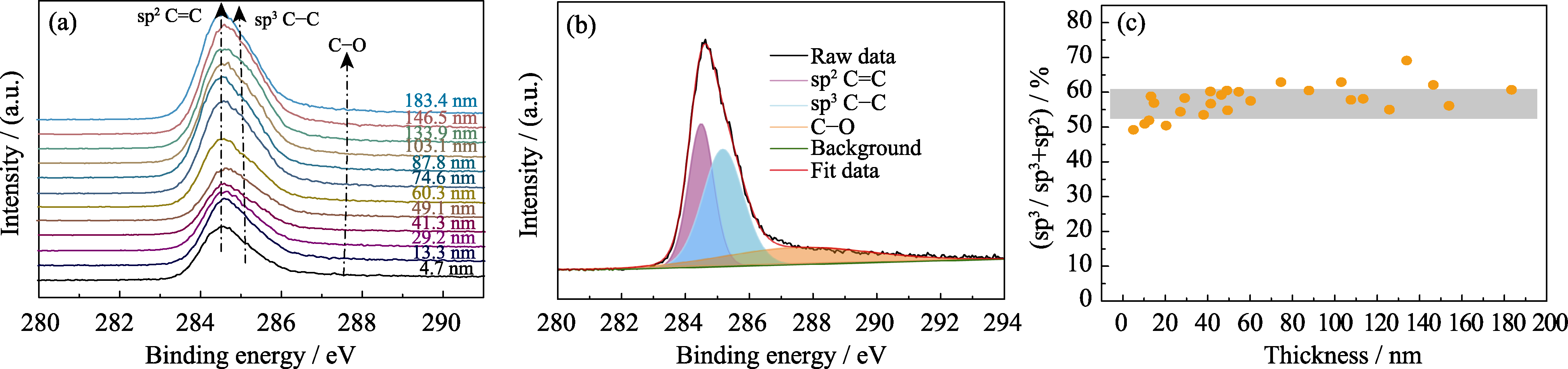
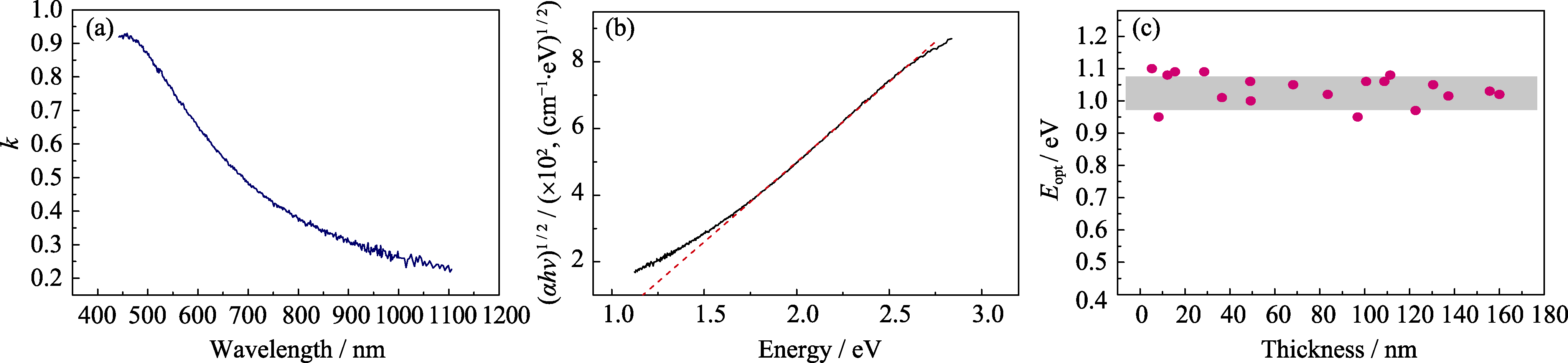
| [1] |
ROBERTSON J.Diamond-like amorphous carbon.Materials Science and Engineering R, 2002, 37(4/5/6): 129-281.
|
| [2] |
ERDEMIR A, FENSKE G R, TERRY J, et al. Effect of source gas and deposition method on friction and wear performance of diamond-like carbon films. Surface and Coatings Technology, 1997, 94-95(1): 525-530.
|
| [3] |
WANG M, JIANG X, STRIZKER B, et al.Adhesion of hydrogenated amorphous carbon films on silicon substrates and its enhancement.Thin Solid Films, 1991, 197(1/2): 57-66.
|
| [4] |
ENKE K.Some new results on the fabrication of and the mechanical, electrical and optical properties of I-carbon layers.Thin Solid Films, 1981, 80(1/2/3): 227-234.
|
| [5] |
PALOMAKI T, WESTER N, CARO M A, et al.Electron transport determines the electrochemical properties of tetrahedral amorphous carbon (ta-C) thin films.Electrochimica Acta, 2017, 225: 1-10.
|
| [6] |
MCCANN R, ROY S S, PAPAKONSTANTINOU P, et al.The effect of thickness and arc current on the structural properties of FCVA synthesised ta-C and ta-C: N films.Diamond and related materials, 2005, 14(3): 983-988.
|
| [7] |
SHEEJA D, TAY B K, LEONG K W, et al.Effect of film thickness on the stress and adhesion of diamond-like carbon coatings.Diamond and Related Materials, 2002, 11(9): 1643-1647.
|
| [8] |
ZAVALEYEV V, WALKOWICZ J, KUZNETSOVA T, et al.The dependence of the structure and mechanical properties of thin ta-C coatings deposited using electromagnetic venetian blind plasma filter on their thickness.Thin Solid Films, 2017, 638: 153-158.
|
| [9] |
LI X W, XU S P, KE P L, et al.Thickness dependence of properties and structure of ultrathin tetrahedral amorphous carbon films: a molecular dynamics simulation.Surface & Coatings Technology, 2014, 258: 938-942.
|
| [10] |
MIYAKE S, KUROSAKA W, OSHIMOTO K.Nanometre scale mechanical properties of extremely thin diamond-like carbon films.Tribology - Materials, Surfaces & Interfaces, 2013, 3(4): 158-164.
|
| [11] |
SUNDARARAJAN S, BHUSHAN B.Development of a continuous microscratch technique in an atomic force microscope and its application to study scratch resistance of ultrathin hard amorphous carbon coatings.Journal of Materials Research, 2001, 16(2): 437-445.
|
| [12] |
MA X G, KOMVOPOULOS K, WAN D, et al.Effects of film thickness and contact load on nanotribological properties of sputtered amorphous carbon thin films.Wear, 2003, 254(10): 1010-1018.
|
| [13] |
LI H B, SUN L L, WU G S, et al.Simulation of magnetic field distribution in doubly-bent filter cathode of vacuum arc film growth setup.Chinese Journal of Vacuum Science and Technology, 2008, 29(3): 614-620.
|
| [14] |
CAI J, YANG W, DAI W, et al.Effect of substrate bias on structure and properties of Ta-C films.China Surface Engineering, 2011, 24(6): 62-67.
|
| [15] |
CAI J, YANG W, KE P L, et al.Influence of Ar flow rate on microstructures and tribological properties of tetrahedral amorphous carbon films.Chinese Journal of Vacuum Science and Technology, 2012, 32(8): 740-745.
|
| [16] |
XU S P, LI X W, HUANG M D, et al. Stress reduction dependent on incident angles of carbon ions in ultrathin tetrahedral amorphous carbon films. Applied Physics Letters, 2014,104(14): 141908-1-4.
|
| [17] |
GUO T, ZUO X, GUO P, et al.Effect of etching process on growth and properties of tetrahedral amorphous carbon film.Surface Technology, 2017, 46(4): 143-149.
|
| [18] |
ZHAO J C.A perspective on the materials genome initiative.Chinese Journal of Nature, 2014, 36(2): 89-104.
|
| [19] |
WANG HAI-ZHOU, WANG HONG, DING HONG, et al.Progress in high-throughput materials synthesis and characterization.Science & Technology Review, 2015, 33(10): 31-49.
|
| [20] |
EVANS J W.Factors mediating smoothness in epitaxial thin-film growth.Physical Review B, 1991, 43(5): 3897-3905.
|
| [21] |
ZHONG M, ZHANG C H, LUO J B.Effect of substrate morphology on the roughness evolution of ultrathin DLC films.Applied Surface Science, 2008, 254(21): 6742-6748.
|
| [22] |
FERRARI A C, ROBERTSON J.Raman spectroscopy of amorphous, nanostructured, diamond-like carbon, and nanodiamond.Philosophical Transactions, 2004, 362(1824): 2477-2512.
|
| [23] |
TAUC J, GRIGOROV R, VANCU A.Optical properties and electronic structure of amorphous germ anium.Phys. Status Solidi, 1966, 15(2): 627-637.
|
| [24] |
薛群基, 王立平. 类金刚石碳基薄膜材料. 北京: 科学出版社, 2012, 585.
|