无机材料学报 ›› 2018, Vol. 33 ›› Issue (6): 587-595.DOI: 10.15541/jim20170527 CSTR: 32189.14.10.15541/jim20170527
• • 下一篇
李汉超1,2,3, 刘盼盼1, 孙丽丽1, 柯培玲1, 崔平1,2, 汪爱英1
收稿日期:2017-11-09
修回日期:2017-12-25
出版日期:2018-06-20
网络出版日期:2018-05-24
作者简介:李汉超(1993-), 男, 博士研究生. E-mail: lihanchao@nimte.ac.cn
基金资助:LI Han-Chao1,2,3, LIU Pan-Pan1, SUN Li-Li1, KE Pei-Ling1, CUI Ping1,2, WANG Ai-Ying1
Received:2017-11-09
Revised:2017-12-25
Published:2018-06-20
Online:2018-05-24
About author:LI Han-Chao. E-mail: lihanchao@nimte.ac.cn
Supported by:摘要:
石墨烯自2004年被首次发现以来, 以其独特、优异的结构和特性引起了广泛关注。目前, 石墨烯的制备已取得了众多进展, 但在大尺寸、高质量、宏量石墨烯可控制备上仍存在挑战, 对制备技术仍需要进行更广泛地探索。非晶碳与石墨烯互为碳的同素异形体, 也可作为制备石墨烯的前驱体, 近些年利用非晶碳制备石墨烯的新颖方法引起了研究学者的兴趣。本文系统论述了利用非晶碳作为固体碳源, 通过金属催化制备大尺寸高质量石墨烯的技术优势, 并着重从金属种类、退火温度、碳源及金属含量比例等方面对石墨烯生成质量的影响进行了阐述。最后, 总结了该方法生长石墨烯的机理, 并对未来的发展方向进行了展望。
中图分类号:
李汉超, 刘盼盼, 孙丽丽, 柯培玲, 崔平, 汪爱英. 金属催化非晶碳转化制备石墨烯方法的研究进展[J]. 无机材料学报, 2018, 33(6): 587-595.
LI Han-Chao, LIU Pan-Pan, SUN Li-Li, KE Pei-Ling, CUI Ping, WANG Ai-Ying. Recent Development of the Transformation from Amorphous Carbon to Graphene Method via Metal Catalyst[J]. Journal of Inorganic Materials, 2018, 33(6): 587-595.
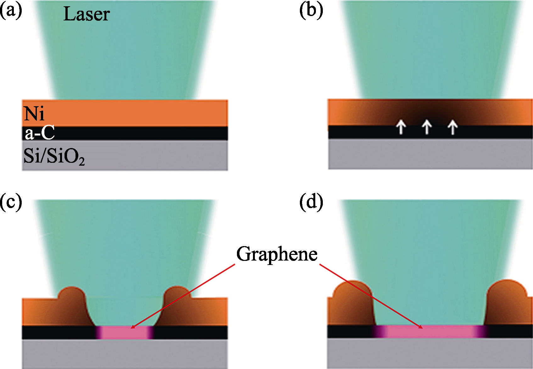
图1 激光照射下石墨烯形成原理图[30]
Fig. 1 Schematic of graphene synthesis mechanism[30](a) Local annealing of the Ni layer by laser irradiation; (b) Dissolution of a-C in the Ni layer; (c) Aggregation and retraction of the Ni layer; (d) Direct graphene synthesis on a SiO2 surface
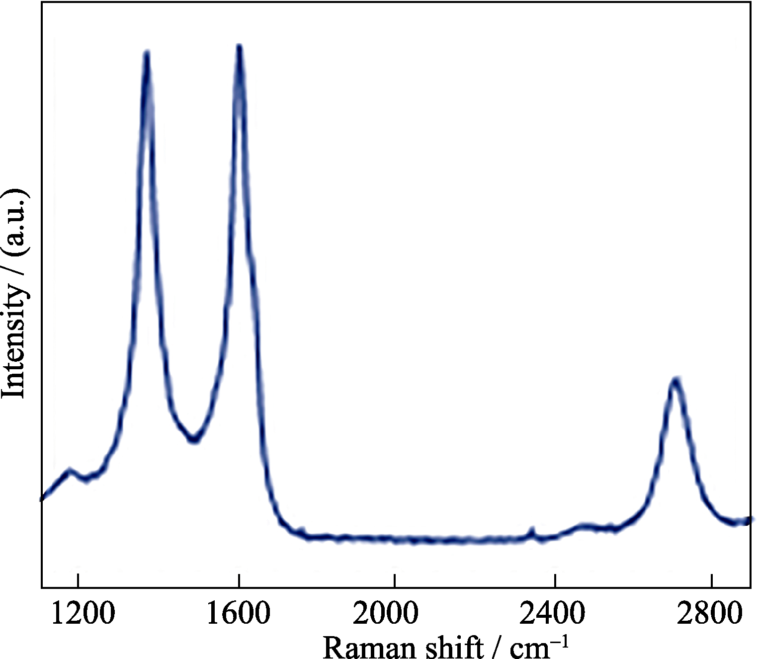
图2 基底200℃、氢气气氛下激光辐照样品的拉曼光谱图[30]
Fig. 2 Raman spectrum for a sample irradiated with a laser in H2 atmosphere at a substrate temperature of 200℃[30]
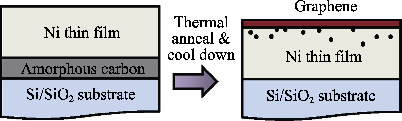
图3 热退火方法金属催化非晶碳转化石墨烯示意图[31]
Fig. 3 Process schematic for the metal-catalyzed crystallization of a-C to graphene by thermal annealing[31]
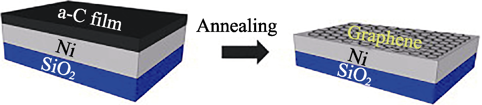
图4 石墨烯生长方法示意图[32]
Fig. 4 Schematic illumination of the graphene growth method[32]
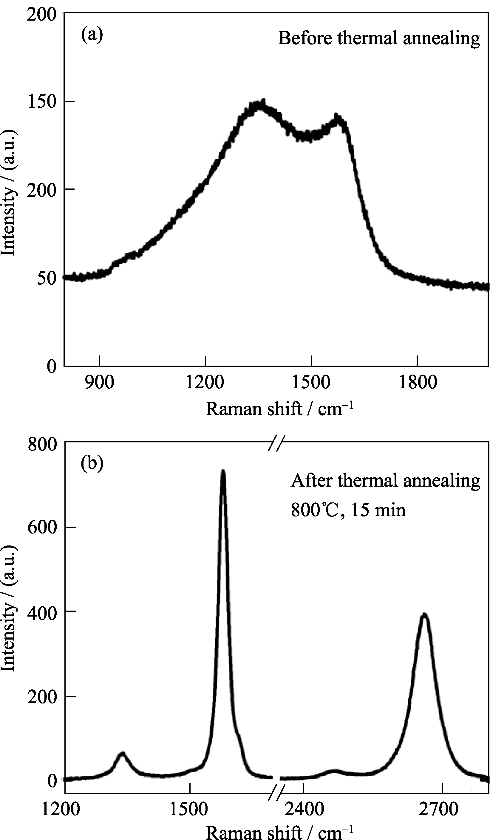
图5 (a) a-C(40 nm)和(b)Ni催化结晶后得到的石墨烯(Ni厚度~300 nm)的Raman光谱图, 激光发射波长632.8 nm[31]
Fig. 5 Raman spectra of (a) a-C (40 nm) and (b) the resulting graphene layer after Ni-catalyzed crystallization (Ni thickness ~300 nm) with excitation laser wavelength 632.8 nm[31]
| a-C method | T/℃ | Annealing time/min | Gas | Catalyst | Pressure/Pa | Graphene morphology | Raman | Ref. | |
|---|---|---|---|---|---|---|---|---|---|
| ID/IG | I2D/IG | ||||||||
| EBE | 650-950 | 15 | Ar | Ni, Co | 226 | Single, double layer | 0.09 | - | [31] |
| FVAD | 600-1000 | 5 | - | Ni | - | Few layer | - | - | [32] |
| PAPD | 700-1000 | 5 | N2 | Co, Ni | - | Multilayer | 0.59 | 1 | [35] |
| LA | 1000 | 30 | - | Ga | 1.33×10⁻² | Few layer | - | - | [36] |
| FIB-CVD | 900-1100 | 30, 60 | - | Ga | - | Three, four layer | - | 0.84 | [37] |
| PLD | 800 | 5 | Ar | Co | 0.1 | Single, double layer | 2.5 | 0.67-1.43 | [39] |
| MS | 750-800 | 5-10 | - | Co, Ni | 3.0×10⁻⁴ | Single, double layer | - | 1.43 | [40] |
| DCMS | 1100 | 2 | Ar | Ni | 0.266 | Single, double layer | - | 2.5 | [46] |
| PAPD | 900 | 5 | N2 | Ni | - | Multilayer | - | - | [42] |
| DCMS | 900 | 30 | - | Ni | 2.66×10⁻⁴ | Single, double layer | 0.03 | 4.8 | [52] |
表1 退火热处理非晶碳转化石墨烯的实验参数及结果
Table 1 Parameters and results of thermal annealing for the experiment of transformation of a-C to graphene
| a-C method | T/℃ | Annealing time/min | Gas | Catalyst | Pressure/Pa | Graphene morphology | Raman | Ref. | |
|---|---|---|---|---|---|---|---|---|---|
| ID/IG | I2D/IG | ||||||||
| EBE | 650-950 | 15 | Ar | Ni, Co | 226 | Single, double layer | 0.09 | - | [31] |
| FVAD | 600-1000 | 5 | - | Ni | - | Few layer | - | - | [32] |
| PAPD | 700-1000 | 5 | N2 | Co, Ni | - | Multilayer | 0.59 | 1 | [35] |
| LA | 1000 | 30 | - | Ga | 1.33×10⁻² | Few layer | - | - | [36] |
| FIB-CVD | 900-1100 | 30, 60 | - | Ga | - | Three, four layer | - | 0.84 | [37] |
| PLD | 800 | 5 | Ar | Co | 0.1 | Single, double layer | 2.5 | 0.67-1.43 | [39] |
| MS | 750-800 | 5-10 | - | Co, Ni | 3.0×10⁻⁴ | Single, double layer | - | 1.43 | [40] |
| DCMS | 1100 | 2 | Ar | Ni | 0.266 | Single, double layer | - | 2.5 | [46] |
| PAPD | 900 | 5 | N2 | Ni | - | Multilayer | - | - | [42] |
| DCMS | 900 | 30 | - | Ni | 2.66×10⁻⁴ | Single, double layer | 0.03 | 4.8 | [52] |
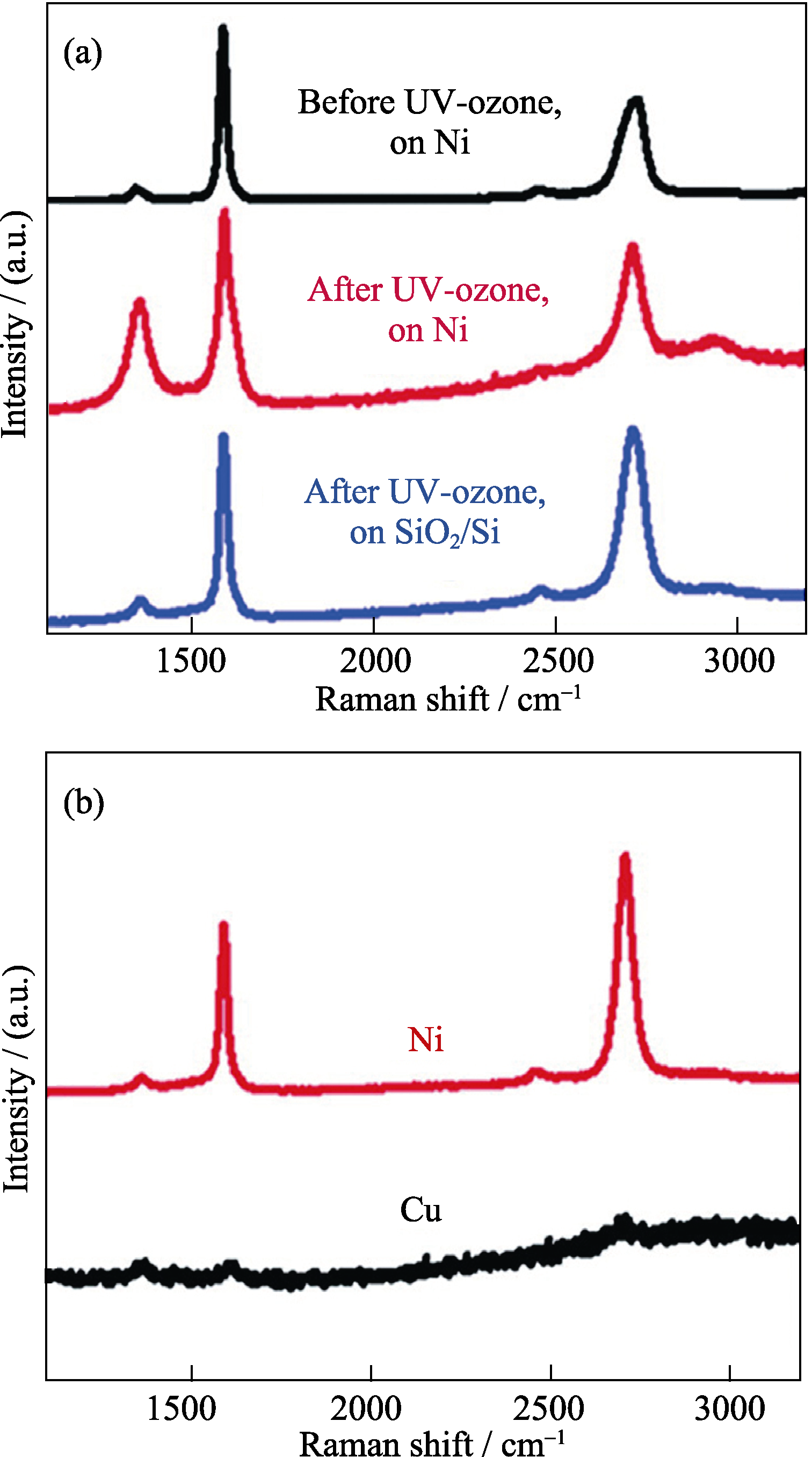
图6 不同生长条件下拉曼分析结果[33]
Fig. 6 Raman spectroscopic analysis of graphene from different growth conditions[33](a) Raman spectra of graphene on the top of the nickel layer before and after UV-ozone exposure, and graphene on the substrate after UV-ozone exposure and nickel removal; (b) Raman spectra of PMMA-derived graphene by different metal catalysts
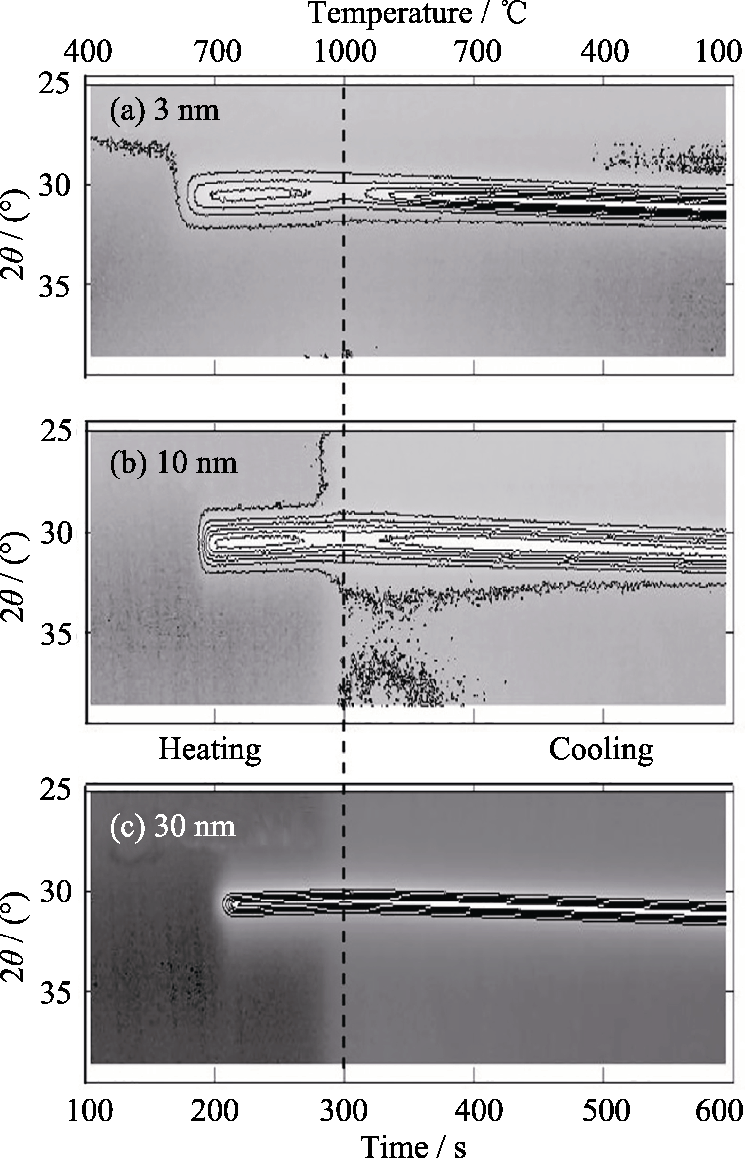
图7 不同厚度Si/SiO2/a-C/Ni(100 nm)样品在He气氛下加热至1000℃及冷却过程中原位XRD的(002)石墨峰强等高线图, 变温速率为3℃/s, 厚度(a) 3 nm、(b) 10 nm和(c) 30 nm。不同厚度a-C样品的等高线间隔不同[41]
Fig. 7 Contour maps of in situ XRD results showing the 002 graphite peak in Si/SiO2/a-C/Ni (100 nm) samples heated to and cooled from 1000℃ in He at a ramp rate of 3℃/s for a-C thicknesses of (a) 3 nm, (b) 10 nm, and (c) 30 nm. The contour lines have a linear intensity spacing that is different for each a-C thickness[41]
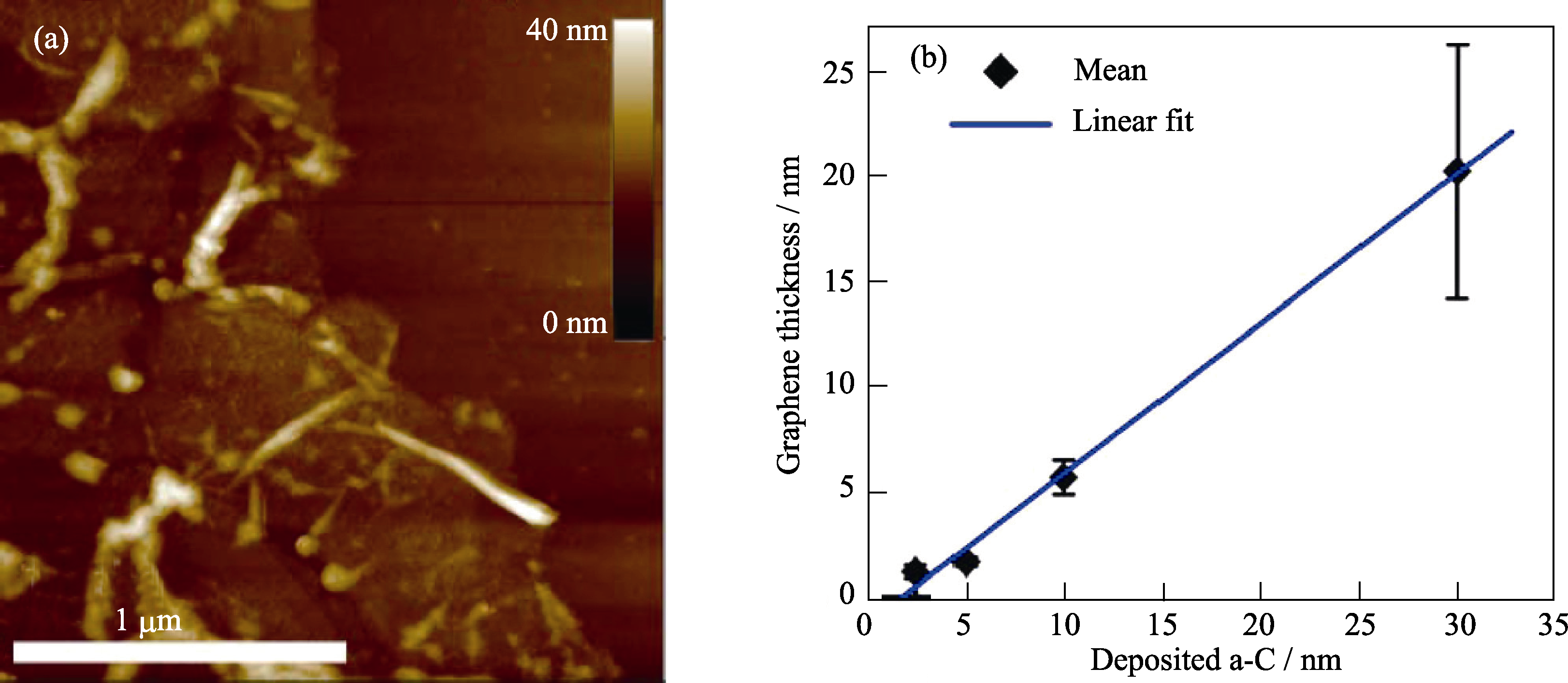
图8 (a)转移到Si/SiO2后的石墨烯AFM照片和(b)石墨烯厚度与原始a-C厚度的关系[31]
Fig. 8 (a) AFM image of a transferred graphene sheet on Si/SiO2 substrate; (b) Graphene (and graphite) thickness vs initial a-C thickness[31] Samples were annealed at 800?℃ for 15 min with a 300 nm Ni catalyst layer
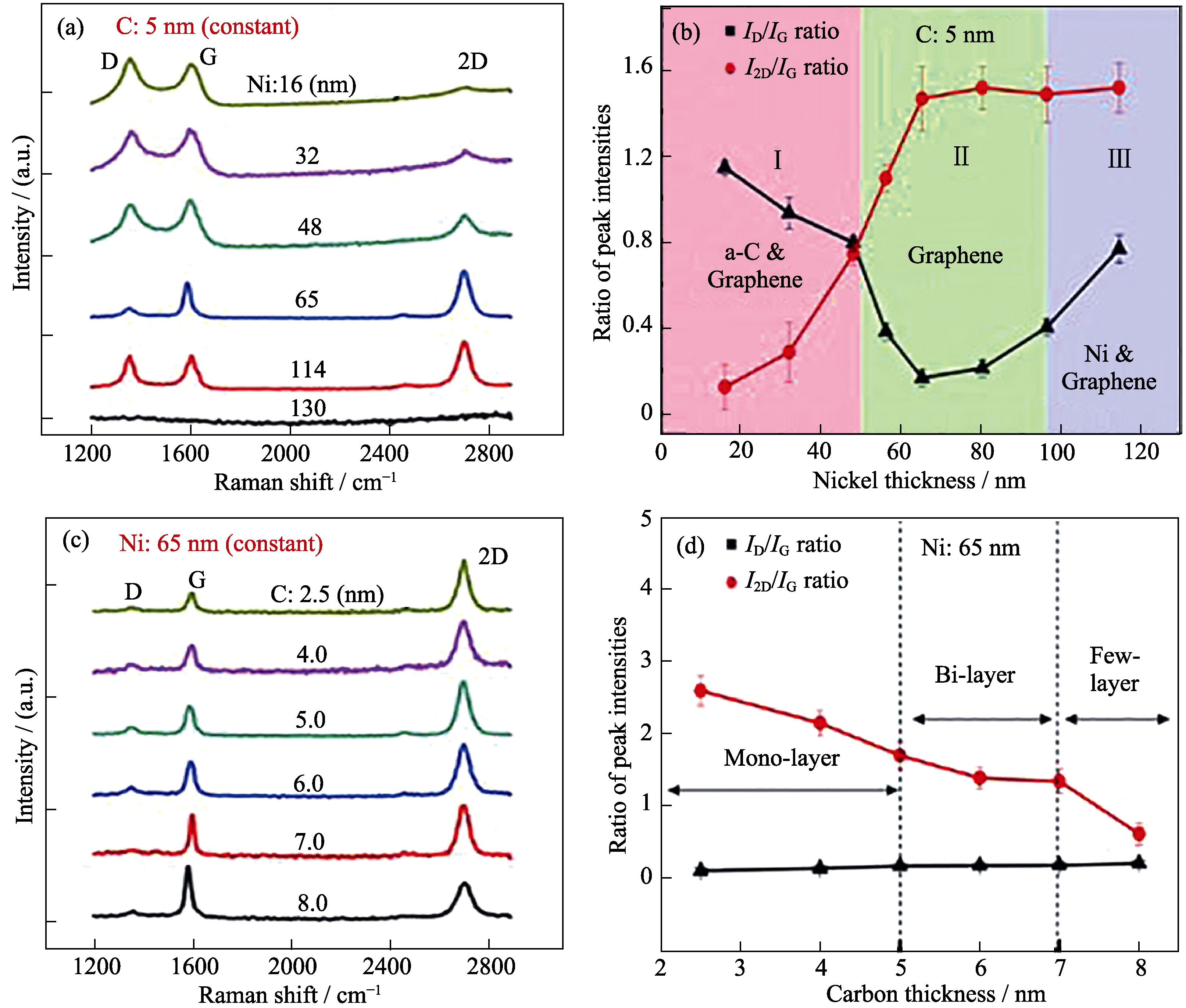
图9 a-C和Ni厚度对石墨烯生长的影响[46]
Fig. 9 Influence of Ni and C film thicknesses on graphene growth[46](a) Raman spectra of RTP graphene grown with a 5 nm C film covered with a Ni film of different thicknesses; (b) ID/IG and I2D/IG Raman peak ratios of the RTP graphene as functions of Ni film thickness; (c) Raman spectra of RTP graphene grown with a 65 nm Ni film on top of a C film with different thicknesses; (d) ID/IG and I2D/IG Raman peak ratios of the RTP graphene as functions of C film thickness
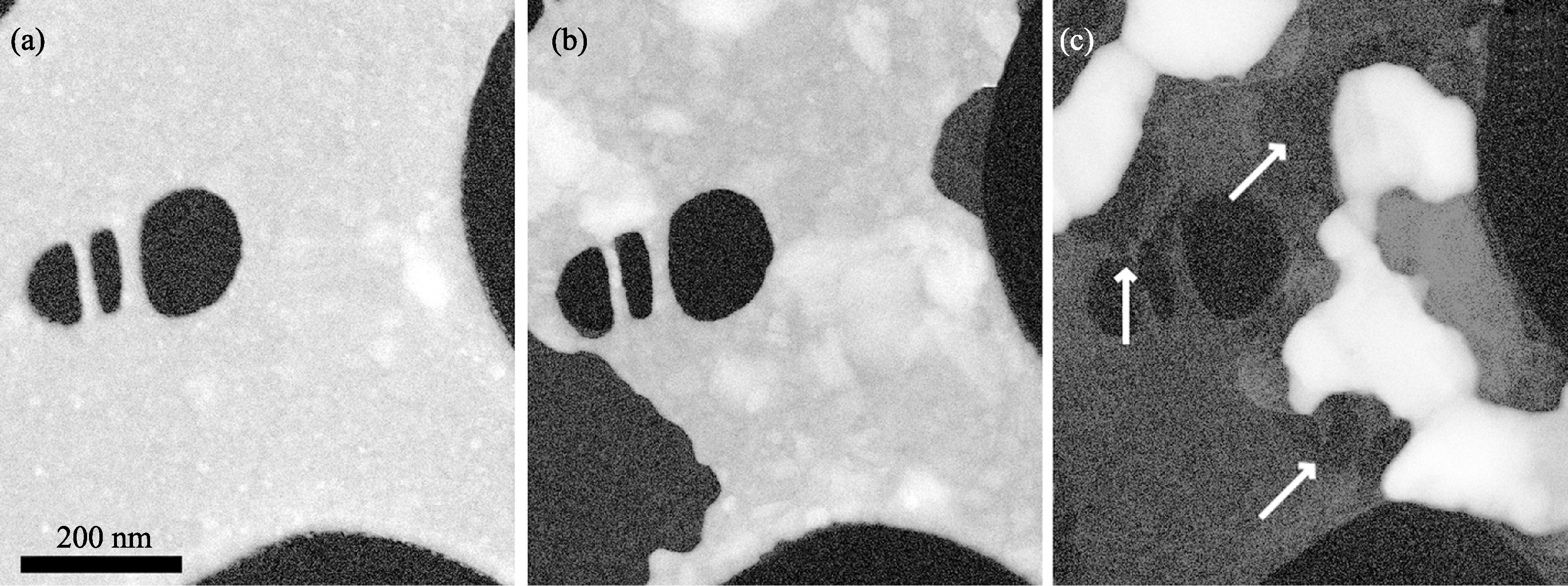
图10 非晶碳上Ni的暗场STEM照片[25]
Fig. 10 Plan-view scanning transmission electron microscopy (STEM) dark-field images of Ni crystals on an amorphous carbon film at 400℃ (a), 600℃ (b) and 720℃ (c) [25](a) At 400℃, the coherent polycrystalline Ni film (bright) covers the C substrate entirely; holes in the C film appear black; (b) At 600℃, ripening of the metal crystals starts and uncovers areas of the amorphous carbon film (light gray contrast); (c) At 720℃, ripening continues and graphene areas appear (dark, marked with arrows)
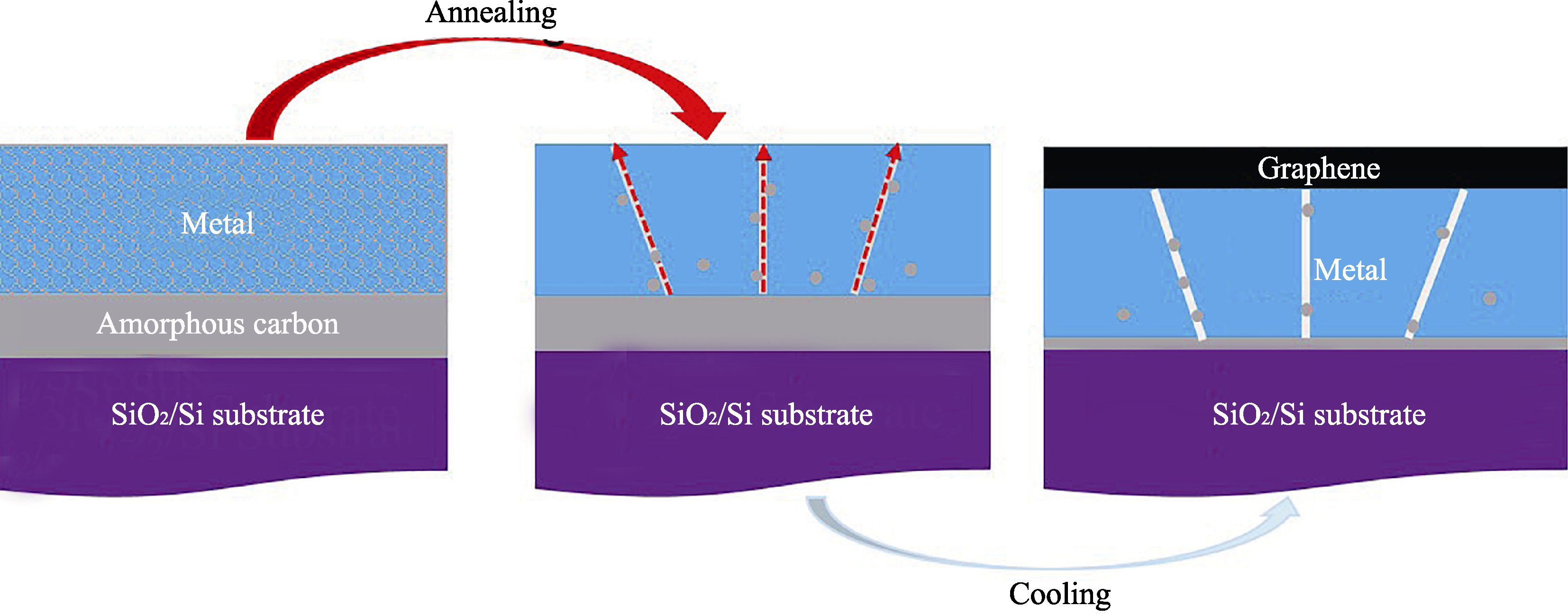
图11 溶解析出形成石墨烯的示意图
Fig. 11 Schematic illustration of graphene formation via C dissolution-precipitation
| [1] | BUNDY F P, HAll H T, STRONG H M,et al. Man-made diamonds. Nature, 1955, 176(4471): 51-55. |
| [2] | AISENBERG S, CHABOT R.Ion-beam deposition of thin films of diamondlike carbon. Journal of Applied Physics, 1971, 42(7): 2953-2958. |
| [3] | KROTO H W, HEATH J R, O'Brien S C,et al. C60: bucminsterfuleene. Nature, 1985, 318(6042): 162-163. |
| [4] | LIJIMA SUMIO.Helical microtubules of graphitic carbon.Nature, 1991, 354(6348): 56-58. |
| [5] | NOVOSELOV K S, GEIM A K, MOROZOV S V,et al. Electric field effect in atomically thin carbon films. Science, 2004, 306(5696): 666-669. |
| [6] | LI G, LI Y, LIU H,et al. Architecture of graphdiyne nanoscale films. Chemical Communications, 2010, 46(19): 3256-3258. |
| [7] | LEE C, WEI X, KYSAR J W,et al. Measurement of the elastic properties and intrinsic strength of monolayer graphene. Science, 2008, 321(5887): 385-388. |
| [8] | NAIR R R, BLAKE P, GRIGORENKO A N,et al. Fine structure constant defines visual transparency of graphene. Science, 2008, 320(5881): 1308. |
| [9] | BALANDIN A A, GHOSH S, BAO W,et al. Superior thermal conductivity of single layer graphene. Nano Letters, 2008, 8(3): 902-907. |
| [10] | MOROZOV S V, NOVOSELOV K S, KATSNELSON M I,et al. Giant intrisic carrier mobilities in graphene and its bilayer. Physical Review Letters, 2008, 100(1): 016602. |
| [11] | OHNO Y, MAEHASHI K, YAMASHIRO Y,et al. Electrolyte- gated graphene field-effect transistors for detecting pH and protein adsorption. Nano Letters, 2009, 9(9): 3318-3322. |
| [12] | YADAV P, BANERJEE A, UNNI S,et al. A 3D hexaporous carbon assembled from single-layer graphene as high performance supercapacitor. ChemSusChem, 2012, 5(11): 2159-2164. |
| [13] | LI S S, TU K H, LIN C C,et al. Solution-processable graphene oxide as an efficient hole transport layer in polymer solar cells. ACS Nano, 2010, 4(6): 3169-3174. |
| [14] | LIN Y M, DIMITRAKOPOULOS C, JENKINS K A,et al. 100-GHz transistors from wafer scale epitaxial graphene. Science, 2010, 327(5966): 662. |
| [15] | EMTSEV K V, BOSTWICK A, HORN K,et al. Towards wafer- size graphene layers by atmospheric pressure graphitization of silicon carbide. Nature Materials, 2009, 8(3): 203-207. |
| [16] | WARNER J H, SCHAFFEL F, RUMMELI M, et al. Graphene: Fundamentals and Emergent Applications. Boston: Newnes, 2012: 204-213. |
| [17] | PARK S, RUOFF R S.Chemical methods for the production of graphenes.Nature Nanotechnology, 2009, 4(4): 217-224. |
| [18] | STANKOVICH S, DIKIN D A, PINER R D,et al. Synthesis of graphene-based nanosheets via chemical reduction of exfoliated graphite oxide. Carbon, 2007, 45(7): 1558-1565. |
| [19] | LI X, CAI W, AN J,et al. Large-area synthesis of high-quality and uniform graphene films on copper foils. Science, 2009, 324(5932): 1312-1314. |
| [20] | 任文才, 高力波, 马来鹏, 等. 石墨烯的化学气相沉积法制备. 新型碳材料, 2011, 26(01): 71-80. |
| [21] | 马来鹏, 任文才, 董再励, 等. 铜表面化学气相沉积石墨烯的研究进展: 生长行为与控制制备. 科学通报, 2012, 57(23): 2158-2163. |
| [22] | KANG J, SHIN D, BAE S,et al. Graphene transfer: key for applications. Nanoscale, 2012, 4(18): 5527-5537. |
| [23] | SUN Z, YAN Z, YAO J,et al. Growth of graphene from solid carbon sources. Nature, 2010, 468(7323): 549-552. |
| [24] | YAN Z, PENG Z, SUN Z,et al. Growth of bilayer graphene on insulating substrates. ACS Nano, 2011, 5(10): 8187-8192. |
| [25] | RODRIGUEZ-MANZO J A, PHAM-HUU C, BANHART F. Graphene growth by a metal catalyzed solid-state transformation of amorphous carbon.ACS Nano, 2011, 5(2): 1529-1534. |
| [26] | 王茂章, 杨全红, 成会明. 碳的结构及其同素异性体. 炭素技术, 2001(1): 23-28. |
| [27] | BAI L, ZHANG G, LU Z,et al. Tribological mechanism of hydrogenated amorphous carbon film against pairs: a physical description. Journal of Applied Physics, 2011, 110(3): 033521. |
| [28] | ROBERTSON J.Diamond-like amorphous carbon.Materials Science and Engineering: R: Reports, 2002, 37(4): 129-281. |
| [29] | DONNET C, ERDEMIR A.Historical developments and new trends in tribological and solid lubricant coatings.Surface and Coatings Technology, 2004, 180: 76-84. |
| [30] | KOSHIDA K, GUMI K, OHNO Y,et al. Position-controlled direct graphene synthesis on silicon oxide surfaces using laser irradiation. Applied Physics Express, 2013, 6(10): 105101. |
| [31] | ZHENG M, TAKEI K, HSIA B,et al. Metal-catalyzed crystallization of amorphous carbon to graphene. Applied Physics Letters, 2010, 96(6): 063110. |
| [32] | SEO J H, LEE H W, KIM J K,et al. Few layer graphene synthesized by filtered vacuum arc system using solid carbon source. Current Applied Physics, 2012, 12: 131-133. |
| [33] | PENG Z W, YAN Z, SUN Z Z,et al. Direct growth of bilayer graphene on SiO2 substrates by carbon diffusion through nickel. ACS Nano, 2011, 5(10): 8241-8247. |
| [34] | LI X, CAI W, COLOMBO L,et al. Evolution of graphene growth on Ni and Cu by carbon isotope labeling. Nano Letters, 2009, 9(12): 4268-4272. |
| [35] | MIYOSHI M, MIZUNO M, BANNO K,et al. Study on transfer- free graphene synthesis process utilizing spontaneous agglomeration of catalytic Ni and Co metals. Materials Research Express, 2015, 2(1): 015602. |
| [36] | FUJITA J, UEKI R, MIYAZAWA Y,et al. Graphitization at interface between amorphous carbon and liquid gallium for fabricating large area graphene sheets. Journal of Vacuum Science & Technology B, 2009, 27(6): 3063-3066. |
| [37] | HATAKEYAMA T, KOMETANI R, WARISAWA S, et al. Selective graphene growth from DLC thin film patterned by focused- ion-beam chemical vapor deposition. Journal of Vacuum Science & Technology B. 2011, 29(6): 06FG04. |
| [38] | WANG J, CHEN L F, WU N,et al. Uniform graphene on liquid metal by chemical vapour deposition at reduced temperature. Carbon, 2016, 96: 799-804. |
| [39] | HIRANO R, MATSUBARA K, KALITA G,et al. Synthesis of transfer-free graphene on an insulating substrate using a solid phase reaction. Nanoscale, 2012, 4(24): 7791-7796. |
| [40] | OROFEO C M, AGO H, HU B,et al. Synthesis of large area, homogeneous, single layer graphene films by annealing amorphous carbon on Co and Ni. Nano Research, 2011, 4(6): 531-540. |
| [41] | SAENGER K L, TSANG J C, BOL A A,et al. In situ X-ray diffraction study of graphitic carbon formed during heating and cooling of amorphous-C/Ni bilayers. Applied Physics Letters, 2010, 96(15): 153105. |
| [42] | BANNO K, MIZUNO M, FUJITA K,et al. Transfer-free graphene synthesis on insulating substrates via agglomeration phenomena of catalytic nickel films. Applied Physics Letters, 2013, 103(8): 082112. |
| [43] | CHU J H, KWAK J, KWON T Y,et al. Facile synthesis of few- layer graphene with a controllable thickness using rapid thermal annealing. ACS Applied Materials & Interfaces, 2012, 4(3): 1777-1782. |
| [44] | WENISCH R, HÜBNER R, MUNNIK F,et al. Nickel-enhanced graphitic ordering of carbon ad-atoms during physical vapor deposition. Carbon, 2016, 100: 656-663. |
| [45] | ANTON R.On the reaction kinetics of Ni with amorphous carbon.Carbon, 2008, 46(4): 656-662. |
| [46] | XIONG W, ZHOU Y S, JIANG L J,et al. Single-step formation of graphene on dielectric surfaces. Advanced Materials, 2013, 25(4): 630-634. |
| [47] | LENG Y, XIE L, LIAO F,et al. Kinetic and thermodynamics studies on the decompositions of Ni3C in different atmospheres. Thermochimica Acta, 2008, 473(1): 14-18. |
| [48] | KOVÁCS G J, BERTÓTI I, RADNÓCZI G. X-ray photoelectron spectroscopic study of magnetron sputtered carbon-nickel composite films.Thin Solid Films, 2008, 516(21): 7942-7946. |
| [49] | ASAKA K, SAITO Y.Spontaneous graphenization of amorphous carbon on clean surfaces of nanometer-sized nickel particles at room temperature.Carbon, 2016, 103: 352-355. |
| [50] | KWAK J, CHU J H, CHOI J K,et al. Near room-temperature synthesis of transfer-free graphene films. Nature Communications, 2012, 3: 645. |
| [51] | 刘盼盼, 李汉超, 杨林等. 退火温度对金属催化四面体非晶碳转变石墨过程的影响. 材料研究学报, 2018. DOI:10.11901/1005.3093.2017.107. |
| [52] | NGUYEN B S, LIN J F, PERNG D C.Non-vacuum growth of graphene films using solid carbon source.Applied Physics Letters, 2015, 106(22): 221604. |
| [53] | CHEN Y Z, MEDINA H, LIN H C,et al. Large-scale and patternable graphene: direct transformation of amorphous carbon film into graphene/graphite on insulators via Cu mediation engineering and its application to all-carbon based devices. Nanoscale, 2015, 7(5): 1678-1687. |
| [54] | SCHNEIDER J J.Transforming amorphous into crystalline carbon: observing how graphene grows.ChemCatChem, 2011, 3(7): 1119-1120. |
| [55] | 张朝华, 付磊, 张艳锋, 等. 石墨烯催化生长中的偏析现象及其调控方法. 化学学报, 2013, 71(03): 308-322. |
| [1] | 孙丽, 徐永善, 高义华. 石墨烯/Bi2O2Se/石墨烯双异质结器件的光探测和仿生突触研究[J]. 无机材料学报, 2026, 41(6): 795-804. |
| [2] | 汪加辉, 刘晶晶, 邱毅, 王永霞, 崔香枝. 原子级铁锚定氮掺杂石墨烯的双功能氧电催化性能[J]. 无机材料学报, 2026, 41(6): 814-822. |
| [3] | 秦英, 姚焯, 郑丽君, 包硕, 李鹏, 郭诗淇. 柔性超级电容器硫掺杂石墨烯/导电聚合物复合电极材料的制备及性能研究[J]. 无机材料学报, 2026, 41(5): 604-610. |
| [4] | 程澳芃, 王跃文, 许文涛, 刘全伟, 张海涛, 周有福. 吸附-沉淀自组装结合放电等离子烧结法制备石墨烯增强氧化铝复合陶瓷[J]. 无机材料学报, 2026, 41(4): 536-544. |
| [5] | 朱开煌, 杨世杰, 李欣格, 宋贯卿, 史淦升, 王焱, 任小孟, 陆遥, 徐新宏, 孙静. 基于UiO-66骨架的氧化石墨烯改性金属有机框架凝胶的制备及其对甲苯的高效吸附性能[J]. 无机材料学报, 2026, 41(4): 519-526. |
| [6] | 范雨竹, 王媛, 王林燕, 向美玲, 鄢雨婷, 黎本慧, 李敏, 文志东, 王海超, 陈永福, 邱会东, 赵波, 周成裕. 氧化石墨烯基吸附材料去除水体中Pb(II): 制备、性能及机理[J]. 无机材料学报, 2026, 41(1): 12-26. |
| [7] | 杨茗凯, 黄泽皑, 周芸霄, 刘彤, 张魁魁, 谭浩, 刘梦颖, 詹俊杰, 陈国星, 周莹. 基于Cu与金属氧化物-KCl熔融介质的甲烷热解制备少层石墨烯与氢气联产研究[J]. 无机材料学报, 2025, 40(5): 473-480. |
| [8] | 高晨光, 孙晓亮, 陈君, 李达鑫, 陈庆庆, 贾德昌, 周玉. 基于湿法纺丝技术的SiBCN-rGO陶瓷纤维的组织结构、力学和吸波性能[J]. 无机材料学报, 2025, 40(3): 290-296. |
| [9] | 王悦, 王欣, 于显利. 室温铁磁性还原氧化石墨烯基全碳膜[J]. 无机材料学报, 2025, 40(3): 305-313. |
| [10] | 李红兰, 张俊苗, 宋二红, 杨兴林. Mo/S共掺杂的石墨烯用于合成氨: 密度泛函理论研究[J]. 无机材料学报, 2024, 39(5): 561-568. |
| [11] | 孙川, 何鹏飞, 胡振峰, 王荣, 邢悦, 张志彬, 李竞龙, 万春磊, 梁秀兵. 含有石墨烯阵列的SiC基陶瓷材料的制备与力学性能[J]. 无机材料学报, 2024, 39(3): 267-273. |
| [12] | 王艳莉, 钱心怡, 沈春银, 詹亮. 石墨烯基介孔锰铈氧化物催化剂: 制备和低温催化还原NO[J]. 无机材料学报, 2024, 39(1): 81-89. |
| [13] | 杨平军, 李铁虎, 李昊, 党阿磊. 石墨烯对环氧树脂泡沫炭石墨化、电导率和力学性能的影响[J]. 无机材料学报, 2024, 39(1): 107-112. |
| [14] | 董怡曼, 谭占鳌. 宽带隙钙钛矿基二端叠层太阳电池复合层的研究进展[J]. 无机材料学报, 2023, 38(9): 1031-1043. |
| [15] | 陈赛赛, 庞雅莉, 王娇娜, 龚䶮, 王锐, 栾筱婉, 李昕. 绿-黄可逆电热致变色织物的制备及其性能[J]. 无机材料学报, 2022, 37(9): 954-960. |
| 阅读次数 | ||||||
|
全文 |
|
|||||
|
摘要 |
|
|||||