

人工视觉系统通常包括用于获取数据的数字图像传感器、用于储存视觉信息的存储单元以及执行图像处理任务的处理单元[4⇓-6]。当前人工视觉系统通过硅基互补金属氧化物半导体(Complementary Metal-oxide Semiconductor, CMOS)图像传感器可以连续不断地实时监测图像, 但是这个过程会产生大量冗余数据, 并占据大量存储空间。此外, 现有的视觉系统处理器不能直接处理光信号, 需要用传感器阵列将光信号转化为电信号, 并将其传递给处理器进行下一步的信号处理, 而信号传递过程会降低处理效率并增加能耗[7-8]。综上所述, 我们迫切需要开发能够集成感知、存储以及处理功能的光电子芯片, 以实现更为高效的人工视觉系统。
人类的视觉系统能够在复杂的环境中对各种物体实现信息感知[9-10]。外界的视觉信息通过视网膜转变为电信号, 再经过视神经传输到大脑, 最终由视觉皮层中的神经网络处理数据形成视觉。在视网膜上, 具有不同功能的神经元相互连接, 形成具有层次的生物学结构。视网膜的主要功能是感知并预处理视觉信息, 进而提取视觉信息的关键特征[11], 这大大提高了人脑的信息处理效率[12]。因此, 在非结构化图像分类以及识别方面, 人类视觉系统的成像以及识别效率远高于人工视觉系统。因此, 类视网膜芯片成为下一代视觉芯片的发展方向, 以期解决传统芯片所面临的挑战[13-14]。到目前为止, 研究人员提出多种技术方案模拟视网膜功能, 将图像传感单元和处理单元集成到每一个像素中, 以实现视网膜功能[15]。光电人工突触器件作为新型视觉芯片的硬件基础[16], 已经成为相关研究热点。这些器件的工作原理包括氧空位的电离和中和、光生载流子的捕获和释放、光致相变以及光与铁电材料相互作用等。本综述将从光电突触器件的工作机理的角度回顾其研究进展。
1 氧空位的电离和解离
图1
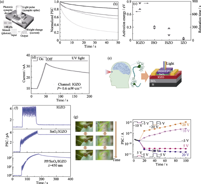
图1
关于氧空位电离和解离机理的研究工作
Fig. 1
Research based on the operation mechanism of ionization and dissociation of oxygen vacancy
(a) Device structure, optical microscope image of an IGZO-based photonic neuromorphic device; (b) Current decaying characteristics of IGZO, ISO, ISZO, and IZO films (from top to bottom) after pulsed UV exposure; (c) Relationship between the activation energy and the relaxation time constant for various amorphous oxide semiconductors; (d) Typical photoinduced current generation and decaying characteristics of IGZO semiconductor upon UV-light exposure[21]; (e) Artificial neuromorphic system for eyesight simulation based on SnOx/IGZO; (f) Current variation and decay of IGZO, SnOx/IGZO devices after 450 nm-light pulse stimulus; (g) Schematic process of the selective memory for the moth and dragonfly image with the time (left panel), and the selective amnesia and memory processes achieved by utilizing 9 positive and negative VGS pulses[20]
Yu等[20]对光激发的氧空位相关的缺陷态密度、光生载流子弛豫的活化能做了进一步研究, 并深入分析了光生载流子与光电突触行为的内在联系。Yu等将宽带隙半导体SnOx覆盖到IGZO上, 并基于此构建了三端薄膜晶体管与p-n结耦合的光电神经形态器件, 进而模拟了光电突触行为(图1(e))。SnOx覆盖后的IGZO器件表现出更为显著的持续光电导特性(图1(f))。值得一提的是, 该光电突触器件的性能取决于光生载流子的产生以及弛豫, 而光生载流子一方面由通道缺陷态的电子捕获和释放决定, 另一方面也受源漏电压和栅极电压的影响, 因此结合两种调控方式可以模拟更复杂的“选择性失忆和记忆行为”(图1(g))。此外, 该器件表现出超低功耗以及全透光性, 这可能对下一代透明光电神经形态器件的研究和应用有重要意义。
2 光生载流子的捕获和释放
氧化物半导体内部存在大量诸如悬空键以及局部扭曲之类的缺陷, 这些缺陷往往充当俘获载流子的陷阱。当氧化物半导体被能量大于禁带宽度的光子激发时, 光生载流子就会被缺陷俘获, 而俘获的光生载流子需要一定时间释放。光生载流子的俘获和释放会导致半导体电导的弛豫性变化, 而这一变化可以用来模拟生物突触中的后突触电流的衰变。而当俘获的光生载流子未完全释放时, 再次对半导体进行激励, 则将占据更低能量的陷阱, 这会导致衰减时间更长, 甚至是非易失性的, 这种物理效应可以用来模拟生物突触长程可塑性。
有机铅卤化物钙钛矿以其出色的光电特性常被用于制备太阳能电池。Yin等[22]将有机铅卤化物钙钛矿(MAPbI3)与硅纳米膜结合形成异质结构, 并将该结构用于制备三端光电突触器件(图2(a))。由于MAPbI3优异的光吸收特性, 基于该异质结构的三端光电突触器件对光激励具有不错的光电响应。Yin等基于该器件的优良特性, 模拟了兴奋突触后电流(EPSC)、双脉冲促进(PPF)等生物突触功能(图2(b, c))。此外, 硅纳米薄膜与MAPbI3形成的p-n结也可以对兴奋突触后电流进行调制, 该调制可以用于模拟生物在不同情况下的视觉学习以及记忆过程(图2(d, e))。除了有机卤化物钙钛矿以外, 无机卤化物钙钛矿材料也被用于光电突触器件。以无机钙钛矿CsPbBr3为例, 它具有窄激子结合能、出色的光吸收特性、高稳定性、高载流子迁移率和长载流子寿命等特点, 使无机钙钛矿CsPbBr3量子点成为光子闪存的潜在候选材料[23-24]。Wang等[25]展示了一种基于CsPbBr3量子点的光电突触器件(图2(f)),并五苯与CsPbBr3量子点的能带排布导致光生空穴从CsPbBr3量子点扩散到并五苯, 而当移除光激励后, 被捕获的载流子电荷依旧可以被势阱保留很长时间(图2(g))。基于此, Wang等实现了短程可塑性、长程可塑性等一系列突触功能(图2(i))。此外, 该器件在相同功率、不同波长的光激励下, 表现出不同的瞬态特性(图2(h))。Wang等利用其差异性, 通过调整波长, 对器件的电导状态进行了编码, 且具有不错的保持特性。
图2
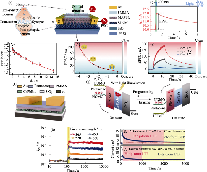
图2
基于光生载流子的捕获和释放机理的研究工作
Fig. 2
Research based on operation mechanism of trapping/detrapping of photogenerated carriers
(a) Schematic of emulating a biological synapse by using a synaptic transistor based on the hybrid structure of Si NM and MAPbI3; (b) EPSC of a synaptic transistor triggered by an optical spike; (c) Dependence of the PPF index (defined as A2/A1) on Δt; (d) Dependence of the maximum EPSC triggered by 30 optical spikes on the backgate voltage; (e) EPSC triggered by 30 optical spikes at various backgate voltages[22]; (f) Schematic illustration of the CsPbBr3 quantum dots-based synapse devices; (g) Schematic energy diagram of the device during light programming operation and during electrical erasing operation under dark condition; (h) Transient characteristic of the synaptic device after light programming operation with fixed light intensity and wavelength varied from 365 to 660 nm; (i) Long-term potentiation (bottom panel) and long-term depressing (top panel) of the CsPbBr3 quantum dots-based synapse devices under different light illumination[25]
3 光致相变
相变器件具有制备技术成熟、集成方便等优点, 非常有利于神经形态器件的高密度集成。光致相变特性可以将相变存储器的这些优点拓展到光电突触器件上来, 对于未来光电突触器件的发展有重要的意义。Ríos等[26]报道了一种基于相变的非易失性多级存储器(图3(a)), 该工作以Ge2Sb2Te5(GST)为光吸收层, 并通过改变GST上所施加的能量使其在结晶相与非晶相之间转变(图3(b))。由于GST与波导传输的光会有倏逝耦合现象, GST的不同结晶状态会导致光传输量发生改变。需要指出的是, 由于晶体状态GST的光吸收率大于非晶态的GST, 因此Ríos等将GST处于晶体状态时的光通过率定义为“0”, 而GST处于非晶态时的光通过率定义为“1”(图3(b))。通过以上方法, 将GST作为信息存储元件, 进而对传输的光量进行编码(图3(c))。该器件的写入和读取过程都是通过相变材料的倏逝耦合来实现, 所以不受衍射极限影响。此外, 该器件读写过程通过使用纳秒光脉冲在波导内实现, 这为快速全光光子突触器件的设计提供了重要思路。
图3
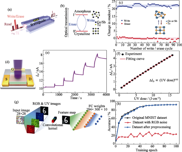
图3
基于光致相变机理的研究工作
Fig. 3
Research based on the operation mechanism of the light-induced phase change
(a) Schematic of the all-optical memory device based on GST; (b) Optical transmission data of the waveguide are encoded by switching between crystalline and amorphous phases GST; (c) Multiple repetitions of the same switching cycle[26]; (d) Schematic illustration of the neuromorphic devices based on VO2 film; (e) ID response to UV irradiation at different durations; (f) Relationship between ΔID and incident UV dose; (g) Realization of neuromorphic preprocessing function to achieve image noise reduction utilizing the sensor array, with the system being spatially divided into a convolution kernel array part for visual information preprocessing and an ANN part for image recognition; (h) Recognition accuracy with and without neuromorphic preprocessing[27]; Colorful figures are available on website
二氧化钒从低温单斜相向高温金红石相的转变过程中展现出数量级的电阻状态和红外光透过率的大幅变化, 这种近室温相变特性使二氧化钒在新型电子和光学器件方面得到广泛应用。Li等[27]提出了一种基于光控制二氧化钒相变的新型神经形态器件(图3(d)), 并利用该器件实现了紫外光感知和多级存储功能(图3(e))。该研究发现, 二氧化钒薄膜单斜晶相的比例会随着紫外辐射计量的增加而降低, 进而实现具有传感和非易失性多级存储特性的光电突触器件(图3(f))。Li等还构建了光电人工神经网络并演示了手写数字图像集的识别(图3(g, h))。基于光致相变的神经形态器件虽然有诸多优势, 但也面临种种挑战。由于温度在相变器件的电阻变化中往往起着非常重要的作用, 因此热管理的作用不可忽视, 尤其对于大规模集成电路。此外, 非晶态的稳定性也需要引起足够重视, 譬如由非晶态到晶体相转变的动力学特性会导致非晶态电阻漂移[28]。
4 光与铁电相互作用
铁电体是具有自发铁电极化的一类材料, 已被广泛应用于非易失性存储器[29]、高介电常数电介质[30]、电光调制器[31]、热释电传感器[32]、压电致动器[33]。铁电材料与电场、应力场、光场等相互作用是铁电材料的研究热点, 也是其器件应用的基础。通过精细的铁电畴调控工程, 铁电材料也可应用于神经形态计算。一般可以通过脉冲电场来调控铁电材料的多级电阻状态[34-35], 其神经形态应用研究主要集中在电子人工突触方面[36⇓⇓-39]。虽然铁电极化反转一般通过施加电场来实现, 但最近越来越多的研究表明机械应力、化学掺杂以及光诱导均可以成为铁电极化调控的手段[40⇓-42], 而这些调控手段也为制备基于铁电材料的多自由度器件提供了新的可能。相比较而言, 光诱导作为一种非接触的调控手段, 一直备受关注, 近几年的研究也表明光诱导可以作为铁电畴调控的有效手段[43]。与电场调控相比, 光诱导可以大大降低对电路设计的要求, 提高切换速 度[44]。目前, 铁电材料在光电突触器件的应用主要利用光致铁电极化反转特性[45]、可反转铁电光伏特性[46-47]等。
目前, 光调控铁电极化反转的研究主要分为两类。一类基于热调控机理, 铁电材料在高功率光照射下, 局部温度会升高到居里温度附近, 进而导致铁电材料局部翻转极化状态[48], 然而这种类型的光致极化切换往往是破坏性的[49]。另一类基于电荷调控机理, 光可以通过能带与能带之间的跃迁产生非平衡载流子, 导致铁电极化失稳甚至发生反转, 这种转变往往无损且可逆。Long等[44]利用铁电薄膜内部本身存在的压印电场以及光伏响应, 在光照下实现了铁电极化翻转(图4(a)), 并发现铁电异质结电阻状态的变化(图4(b))。Li等[43]在多层二硫化钼与铁电薄膜的异质结中发现了光致铁电极化反转现象(图4(c, d))。与铁电薄膜直接光吸收导致的铁电极化反转相比, 二维材料/铁电异质结可以大大降低所需的激光能量, 激光功率密度降低至1 mW/cm2量级[45,50-51]。Luo等[45]利用二维材料/铁电异质结的光致极化反转特性, 制备了基于二维材料的铁电场效应晶体管, 并实现了铁电晶体管的多级电阻状态, 初步研究了其光电突触特性(图4(e, f))。
图4
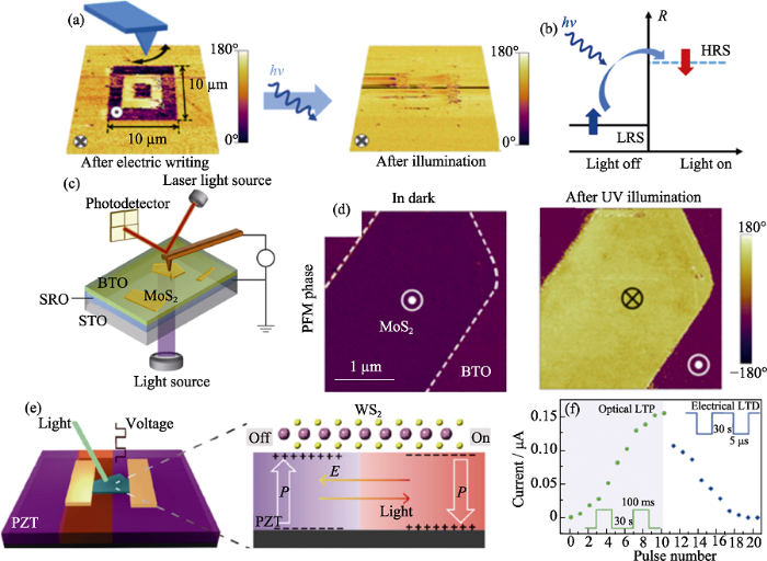
图4
基于光与铁电材料相互作用的研究工作
Fig. 4
Research based on the interaction between light and ferroelectric materials
(a) PFM phase-maps (30 μm×30 μm) of BaTiO3 film, with PDOWN and PUP regions being written by applying voltage to the tip of −8 or +8 V, respectively, but after illumination (blue laser, 10 min) PUP domains being switched back; (b) Low-resistance state (LRS) to high-resistance state (HRS) switching promoted by optically induced polarization reversal[44]; (c) Sketch of the experiment geometry; (d) PFM phase images acquired in the dark before and after UV illumination, showing the MoS2 flake boundary by the dashed lines[43]; (e) Schematic configuration of the device and the mechanism behind the optically and electrically tunable channel conductance; (f) Long-term optical potentiation and electrical depression in the WS2/ PZT optoelectronic synapses[45]
Du等[50]研究了MoS2/BaTiO3铁电晶体管的光致铁电翻转特性, 通过微加工方法制备了光电突触阵列。在单个突触器件中, 单层二硫化钼作为沟道材料, 铁电薄膜材料BaTiO3作为栅极电介质(图5(a))。研究发现二硫化钼和BaTiO3存在共生相互作用, 即一方面BaTiO3的铁电极化方向对单层二硫化钼的电导有显著的调制作用(开关比107)(图5(c));另一方面二维材料的光吸收会导致界面的正电荷积累, 进而促使极化方向从向上翻转为向下。基于MoS2/BaTiO3异质结的光致铁电翻转特性, 覆盖二硫化钼的BaTiO3薄膜在光激励下会从铁电极化向上翻转为铁电极化向下, 而反转过程中的多畴共存现象为器件多级电导态的实现提供了可能(图5(b)), 并可以应用于神经形态计算。Du等还发现对于不同波长的光, 该器件的铁电极化反转速率和程度会有所不同。通过器件对于不同波长光响应的差异, 该团队实现了对图像中蓝色信息的高效提取。此外, 他们还演示了对手写数字图像的降噪与识别, 通过这种神经形态预处理可以将图像识别率由降噪前的15%提高到降噪之后的91%(图5(e, f))。
图5
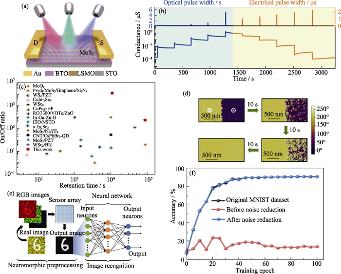
图5
基于光与铁电材料相互作用的研究工作[50]
Fig. 5
Research based on the interaction between light and ferroelectric materials[50]
(a) Schematic illustration of optoelectronic synapses based on MoS2/ BaTiO3; (b) Non-volatile multi-level conductance switching under optical excitation and electrical excitation; (c) Summary of the On/Off ratio and retention time for various optoelectronic synapses reported previously; (d) PFM phase diagrams of the MoS2/ BaTiO3 heterostructure as a function of the light exposure time; (e) Preprocess of the image noise reduction utilizing the sensor array; (f) Comparisons of the recognition accuracy of the pre-prepared images
5 结束语
本文总结并讨论了光电人工突触的最新研究进展, 并对其工作机理进行了分类讨论。光电人工突触工作机理大致可分为四类, 包括氧空位的电离和解离、光生载流子的捕获和释放、光致相变以及光与铁电材料的相互作用。需要说明的是, 基于上述工作机理的器件各有利弊, 都值得进一步深入研究。对氧空位的电离和解离机制来说, 虽然光照会使氧化物半导体中的氧空位电离, 但是温度也会影响氧空位的迁移,进而影响突触性能, 因此, 热管理是其面临的重要挑战。而对于光致相变机制来说, 虽然相变材料具有优异的存储能力, 并被认为是光电突触器件的有力候选者, 但是非晶态向结晶相转变的动力学特性会导致非晶态电阻漂移问题。对于光生载流子的捕获和释放机制来说, 可以通过能带结构设计来优化突触器件性能, 与前两种机理相比, 设计的混合结构具有其组成材料的优点, 在协同效应作用下可以产生更高的光学灵敏度和更低的功耗, 但由于光生载流子的复合, 其保持特性往往较差。而对于铁电材料来说, 其切换速度超快以及调控能力出色, 但是氧空位对其器件性能有重要影响, 不但会产生漏电, 而且氧空位移动和集聚还会破坏铁电材料局部结构, 进而影响其铁电性。
尽管光电人工突触器件面临很多挑战, 但是其具有电子突触器件所不具备的优势, 即宽带宽、小电阻-电容延迟、低功耗以及全局调节等优点, 并且人工光电突触器件集光电传感和突触功能于一体, 因此在神经形态计算、视觉信息处理等方面展现出巨大优势, 且在人工智能、虚拟现实交互以及物联网领域具有潜在的应用前景。
参考文献
Skin-integrated wireless haptic interfaces for virtual and augmented reality
Artificial sensory memory
Fully photon modulated heterostructure for neuromorphic computing
Digital cameras with designs inspired by the arthropod eye.
Biologically inspired artificial compound eyes

This work presents the fabrication of biologically inspired artificial compound eyes. The artificial ommatidium, like that of an insect's compound eyes, consists of a refractive polymer microlens, a light-guiding polymer cone, and a self-aligned waveguide to collect light with a small angular acceptance. The ommatidia are omnidirectionally arranged along a hemispherical polymer dome such that they provide a wide field of view similar to that of a natural compound eye. The spherical configuration of the microlenses is accomplished by reconfigurable microtemplating, that is, polymer replication using the deformed elastomer membrane with microlens patterns. The formation of polymer waveguides self-aligned with microlenses is also realized by a self-writing process in a photosensitive polymer resin. The angular acceptance is directly measured by three-dimensional optical sectioning with a confocal microscope, and the detailed optical characteristics are studied in comparison with a natural compound eye.
A bioinspired flexible organic artificial afferent nerve
The distributed network of receptors, neurons, and synapses in the somatosensory system efficiently processes complex tactile information. We used flexible organic electronics to mimic the functions of a sensory nerve. Our artificial afferent nerve collects pressure information (1 to 80 kilopascals) from clusters of pressure sensors, converts the pressure information into action potentials (0 to 100 hertz) by using ring oscillators, and integrates the action potentials from multiple ring oscillators with a synaptic transistor. Biomimetic hierarchical structures can detect movement of an object, combine simultaneous pressure inputs, and distinguish braille characters. Furthermore, we connected our artificial afferent nerve to motor nerves to construct a hybrid bioelectronic reflex arc to actuate muscles. Our system has potential applications in neurorobotics and neuroprosthetics.Copyright © 2018 The Authors, some rights reserved; exclusive licensee American Association for the Advancement of Science. No claim to original U.S. Government Works.
Flexible three-dimensional artificial synapse networks with correlated learning and trainable memory capability
Reservoir computing using dynamic memristors for temporal information processing
Reservoir computing systems utilize dynamic reservoirs having short-term memory to project features from the temporal inputs into a high-dimensional feature space. A readout function layer can then effectively analyze the projected features for tasks, such as classification and time-series analysis. The system can efficiently compute complex and temporal data with low-training cost, since only the readout function needs to be trained. Here we experimentally implement a reservoir computing system using a dynamic memristor array. We show that the internal ionic dynamic processes of memristors allow the memristor-based reservoir to directly process information in the temporal domain, and demonstrate that even a small hardware system with only 88 memristors can already be used for tasks, such as handwritten digit recognition. The system is also used to experimentally solve a second-order nonlinear task, and can successfully predict the expected output without knowing the form of the original dynamic transfer function.
Ultrafast machine vision with 2D material neural network image sensors
Short-term plasticity and long-term potentiation mimicked in single inorganic synapses
Memory is believed to occur in the human brain as a result of two types of synaptic plasticity: short-term plasticity (STP) and long-term potentiation (LTP; refs 1-4). In neuromorphic engineering, emulation of known neural behaviour has proven to be difficult to implement in software because of the highly complex interconnected nature of thought processes. Here we report the discovery of a Ag(2)S inorganic synapse, which emulates the synaptic functions of both STP and LTP characteristics through the use of input pulse repetition time. The structure known as an atomic switch, operating at critical voltages, stores information as STP with a spontaneous decay of conductance level in response to intermittent input stimuli, whereas frequent stimulation results in a transition to LTP. The Ag(2)S inorganic synapse has interesting characteristics with analogies to an individual biological synapse, and achieves dynamic memorization in a single device without the need of external preprogramming. A psychological model related to the process of memorizing and forgetting is also demonstrated using the inorganic synapses. Our Ag(2)S element indicates a breakthrough in mimicking synaptic behaviour essential for the further creation of artificial neural systems that emulate characteristics of human memory.
Human eye-inspired soft optoelectronic device using high-density MoS2-graphene curved image sensor array
Optoelectronic resistive random access memory for neuromorphic vision sensors
Neuromorphic visual systems have considerable potential to emulate basic functions of the human visual system even beyond the visible light region. However, the complex circuitry of artificial visual systems based on conventional image sensors, memory and processing units presents serious challenges in terms of device integration and power consumption. Here we show simple two-terminal optoelectronic resistive random access memory (ORRAM) synaptic devices for an efficient neuromorphic visual system that exhibit non-volatile optical resistive switching and light-tunable synaptic behaviours. The ORRAM arrays enable image sensing and memory functions as well as neuromorphic visual pre-processing with an improved processing efficiency and image recognition rate in the subsequent processing tasks. The proof-of-concept device provides the potential to simplify the circuitry of a neuromorphic visual system and contribute to the development of applications in edge computing and the internet of things.
Small footprint transistor architecture for photoswitching logic and in situ memory
Artificial retinas — fast, versatile image processors
Curved neuromorphic image sensor array using a MoS2-organic heterostructure inspired by the human visual recognition system
A ferrite synaptic transistor with topotactic transformation
Electrolyte-gated synaptic transistor with oxygen ions
Gating-induced reversible HxVO2 phase transformations for neuromorphic computing
Optoelectronic neuromorphic thin-film transistors capable of selective attention and with ultra-low power dissipation
Brain-inspired photonic neuromorphic devices using photodynamic amorphous oxide semiconductors and their persistent photoconductivity
Optically stimulated synaptic devices based on the hybrid structure of silicon nanomembrane and perovskite
Optoelectronic synaptic devices have been attracting increasing attention due to their critical role in the development of neuromorphic computing based on optoelectronic integration. Here we start with silicon nanomembrane (Si NM) to fabricate optoelectronic synaptic devices. Organolead halide perovskite (MAPbI) is exploited to form a hybrid structure with Si NM. We demonstrate that synaptic transistors based on the hybrid structure are very sensitive to optical stimulation with low energy consumption. Synaptic functionalities such as excitatory post-synaptic current (EPSC), paired-pulse facilitation, and transition from short-term memory to long-term memory (LTM) are all successfully mimicked by using these optically stimulated synaptic transistors. The backgate-enabled tunability of the EPSC of these devices further leads to the LTM-based mimicking of visual learning and memory processes under different mood states. This work contributes to the development of Si-based optoelectronic synaptic devices for neuromorphic computing.
Quantum dot light-emitting diodes based on inorganic perovskite cesium lead halides (CsPbX3)
Song, Jizhong; Li, Jianhai; Li, Xiaoming; Xu, Leimeng; Dong, Yuhui; Zeng, Haibo Nanjing Univ Sci & Technol, Sch Mat Sci & Engn, Herbert Gleiter Inst Nanosci, Inst Optoelect & Nanomat, Nanjing 210094, Jiangsu, Peoples R China.
Synergies of electrochemical metallization and valance change in all-inorganic perovskite quantum dots for resistive switching
Photonic synapses based on inorganic perovskite quantum dots for neuromorphic computing
Integrated all-photonic non-volatile multi-level memory
Rios, Carlos; Hosseini, Peiman; Bhaskaran, Harish Univ Oxford, Dept Mat, Oxford OX1 3PH, England. Stegmaier, Matthias; Wang, Di; Scherer, Torsten; Pernice, Wolfram H. P. Karlsruhe Inst Technol, Inst Nanotechnol, D-76344 Eggenstein Leopoldshafen, Germany. Wang, Di; Scherer, Torsten Karlsruhe Inst Technol, Karlsruhe Nano Micro Facil, D-76344 Eggenstein Leopoldshafen, Germany. Wright, C. David Univ Exeter, Dept Engn, Exeter EX4 4QF, Devon, England. Pernice, Wolfram H. P. Univ Munster, Inst Phys, D-48149 Munster, Germany.
Photo-induced non-volatile VO2 phase transition for neuromorphic ultraviolet sensors
Emerging memory devices for neuromorphic computing
Ferroelectric memories
In the past year it has become possible to fabricate ferroelectric thin-film memories onto standard silicon integrated circuits that combine very high speed (30-nanosecond read/erase/rewrite operation), 5-volt standard silicon logic levels, very high density (2 by 2 micrometer cell size), complete nonvolatility (no standby power required), and extreme radiation hardness. These ferroelectric random-access memories are expected to replace magnetic core memory, magnetic bubble memory systems, and electrically erasable read-only memory for many applications. The switching kinetics of these films, 100 to 300 nanometers thick, are now well understood, with switching times that fit an activation field dependence that scales applied field and temperature. Earlier problems of fatigue and retention failure are also now understood and have been improved to acceptable levels.
Alternative interpretations for decreasing voltage with increasing charge in ferroelectric capacitors
Large pockels effect in micro-and nanostructured barium titanate integrated on silicon
Surface pyroelectricity in cubic SrTiO3
Monolithically integrated microelectromechanical systems for on-chip strain engineering of quantum dots
Elastic strain fields based on single crystal piezoelectric elements represent an effective way for engineering the quantum dot (QD) emission with unrivaled precision and technological relevance. However, pioneering researches in this direction were mainly based on bulk piezoelectric substrates, which prevent the development of chip-scale devices. Here, we present a monolithically integrated Microelectromechanical systems (MEMS) device with great potential for on-chip quantum photonic applications. High-quality epitaxial PMN-PT thin films have been grown on SrTiO3 buffered Si and show excellent piezoelectric responses. Dense arrays of MEMS with small footprints are then fabricated based on these films, forming an on-chip strain tuning platform. After transferring the QD-containing nanomembranes onto these MEMS, the nonclassical emissions (e.g., single photons) from single QDs can be engineered by the strain fields. We envision that the strain tunable QD sources on the individually addressable and monolithically integrated MEMS pave the way toward complex quantum photonic applications on chip.
Reproducible ultrathin ferroelectric domain switching for high-performance neuromorphic computing
Large-scale Hf0.5Zr0.5O2 membranes with robust ferroelectricity
Learning through ferroelectric domain dynamics in solid-state synapses
Reproducible ultrathin ferroelectric domain switching for high-performance neuromorphic computing
Epitaxial ferroelectric Hf0.5Zr0.5O2 thin films and their implementations in memristors for brain-inspired computing
Reversible chemical switching of a ferroelectric film
Mechanical writing of ferroelectric polarization
Ferroelectric materials are characterized by a permanent electric dipole that can be reversed through the application of an external voltage, but a strong intrinsic coupling between polarization and deformation also causes all ferroelectrics to be piezoelectric, leading to applications in sensors and high-displacement actuators. A less explored property is flexoelectricity, the coupling between polarization and a strain gradient. We demonstrate that the stress gradient generated by the tip of an atomic force microscope can mechanically switch the polarization in the nanoscale volume of a ferroelectric film. Pure mechanical force can therefore be used as a dynamic tool for polarization control and may enable applications in which memory bits are written mechanically and read electrically.
Mechanical switching of ferroelectric domains beyond flexoelectricity
Optical control of polarization in ferroelectric heterostructures
In the ferroelectric devices, polarization control is usually accomplished by application of an electric field. In this paper, we demonstrate optically induced polarization switching in BaTiO3-based ferroelectric heterostructures utilizing a two-dimensional narrow-gap semiconductor MoS2 as a top electrode. This effect is attributed to the redistribution of the photogenerated carriers and screening charges at the MoS2/BaTiO3 interface. Specifically, a two-step process, which involves formation of intra-layer excitons during light absorption followed by their decay into inter-layer excitons, results in the positive charge accumulation at the interface forcing the polarization reversal from the upward to the downward direction. Theoretical modeling of the MoS2 optical absorption spectra with and without the applied electric field provides quantitative support for the proposed mechanism. It is suggested that the discovered effect is of general nature and should be observable in any heterostructure comprising a ferroelectric and a narrow gap semiconductor.
Non-volatile optical switch of resistance in photoferroelectric tunnel junctions
Artificial optoelectronic synapses based on ferroelectric field-effect enabled 2D transition metal dichalcogenide memristive transistors
Ferroelectric photosensor network: an advanced hardware solution to real-time machine vision
Self-driven visible-blind photodetector based on ferroelectric perovskite oxides
Direct writing of ferroelectric domains on the x-and y-faces of lithium niobate using a continuous wave ultraviolet laser
Studies of optical damage in lithium niobate in the presence of thermal gradients
A robust neuromorphic vision sensor with optical control of ferroelectric switching
