), 葛琛2,3()
), GE Chen2,3()
), 葛琛2,3()
), GE Chen2,3()
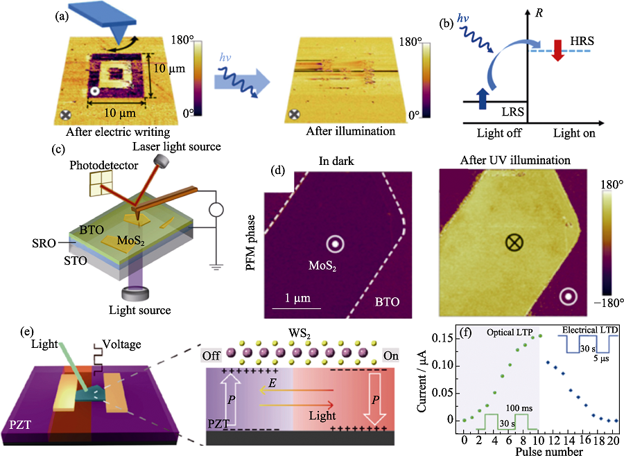
图4. 基于光与铁电材料相互作用的研究工作
Fig. 4. Research based on the interaction between light and ferroelectric materials
(a) PFM phase-maps (30 μm×30 μm) of BaTiO3 film, with PDOWN and PUP regions being written by applying voltage to the tip of −8 or +8 V, respectively, but after illumination (blue laser, 10 min) PUP domains being switched back; (b) Low-resistance state (LRS) to high-resistance state (HRS) switching promoted by optically induced polarization reversal[