Journal of Inorganic Materials ›› 2024, Vol. 39 ›› Issue (9): 1063-1069.DOI: 10.15541/jim20240094
Special Issue: 【信息功能】敏感陶瓷(202512)
Previous Articles Next Articles
YANG Jialin1( ), WANG Liangjun1, RUAN Siyuan1, JIANG Xiulin2,3, YANG Chang1()
Received:2024-03-01
Revised:2024-04-09
Published:2024-09-20
Online:2024-04-19
Contact:
YANG Chang, professor. E-mail: cyang@phy.ecnu.edu.cnAbout author:YANG Jialin (1998-), female, Master candidate. E-mail: 51214700087@stu.ecnu.edu.cn
Supported by:CLC Number:
YANG Jialin, WANG Liangjun, RUAN Siyuan, JIANG Xiulin, YANG Chang. Highly Weak-light Sensitive and Dual-band Switchable Photodetector Based on CuI/Si Unilateral Heterojunction[J]. Journal of Inorganic Materials, 2024, 39(9): 1063-1069.
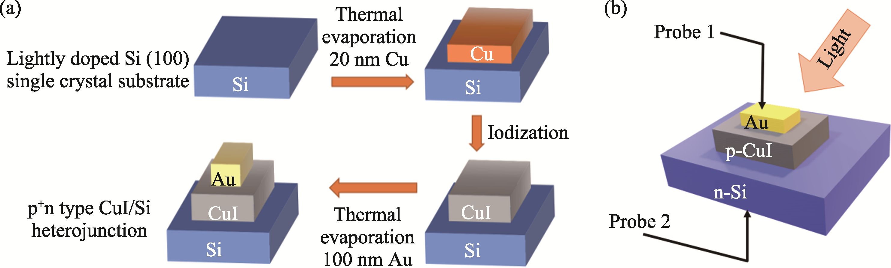
Fig. 1 Fabrication and testing schematic diagram (a) Schematic structure of the fabricated p+n type CuI/Si heterojunction diode; (b) Schematic diagram of the photodiode test
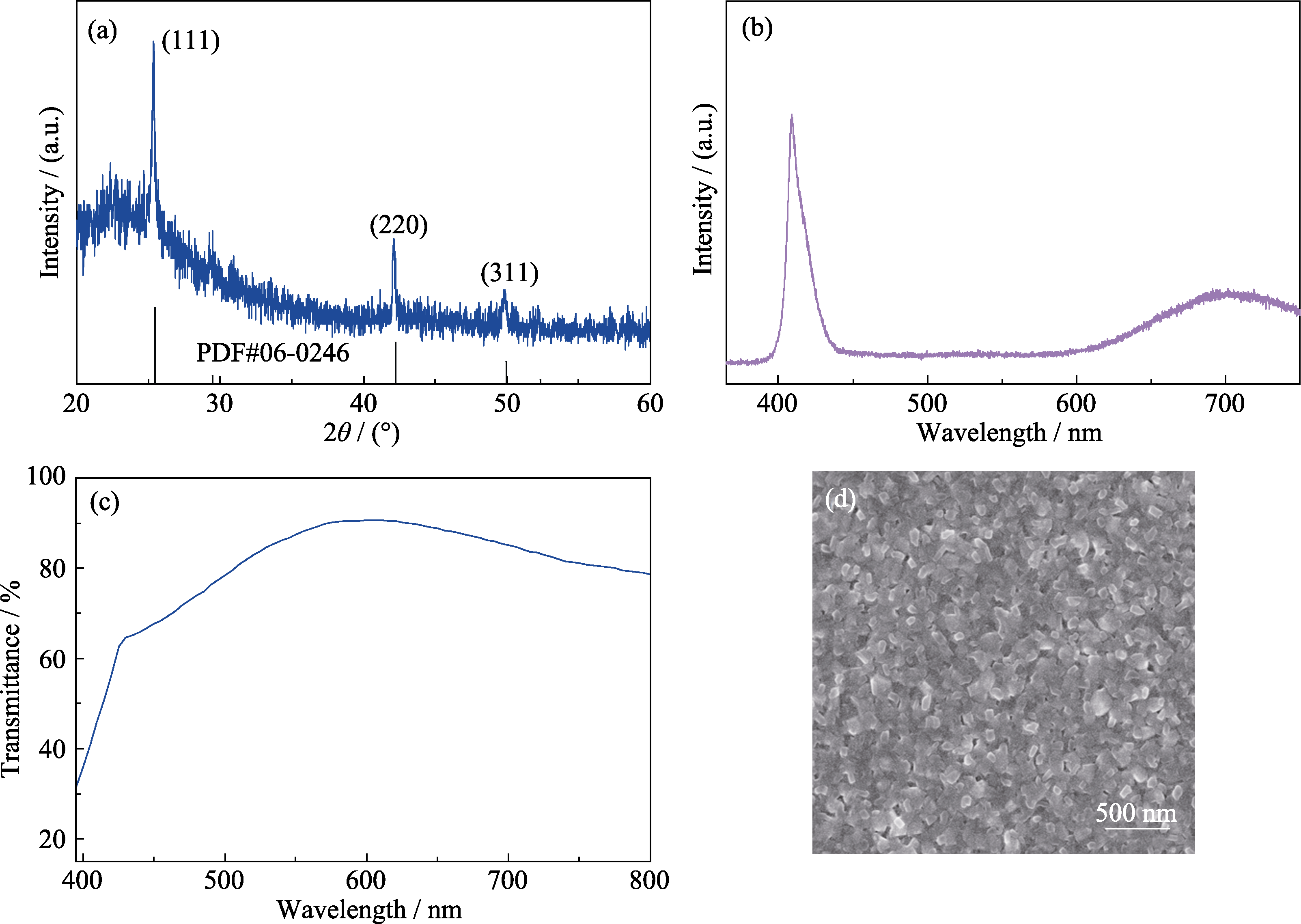
Fig. 2 Structural and electrical characterization of the obtained CuI thin film (a) XRD pattern; (b) PL spectrum; (c) Optical transmittance; (d) SEM image
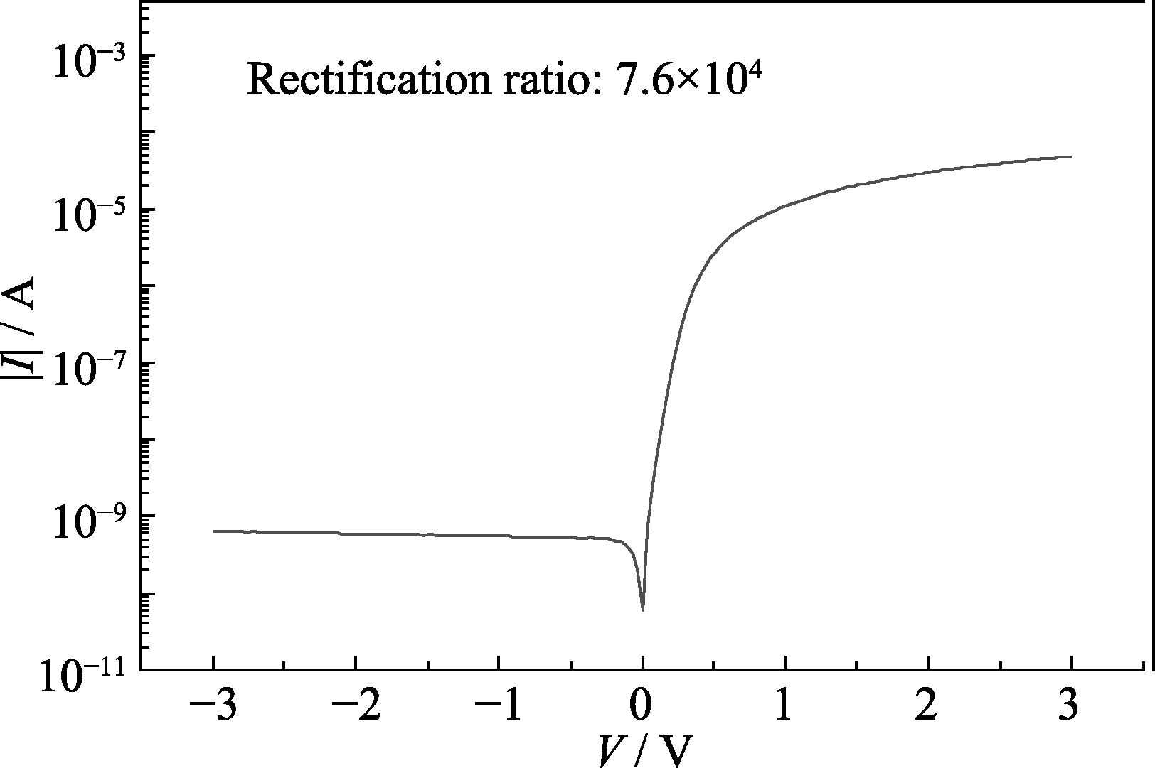
Fig. 3 I-V characteristic curve of the CuI/Si heterojunction
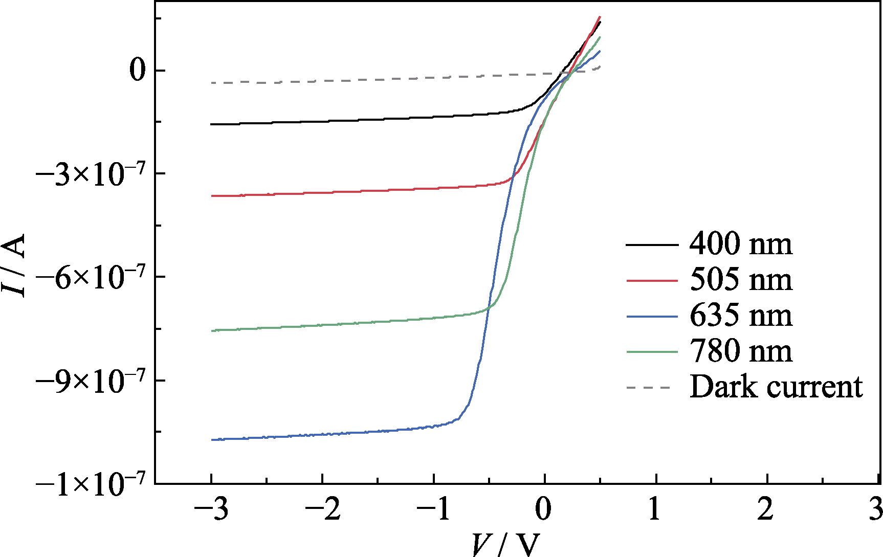
Fig. 4 I-V characteristic curves of the CuI/Si photodiode under different laser light wavelengths with a light power density of 50 μW/cm2 Dark current is plotted in dashed line; Colorful figure is available on website
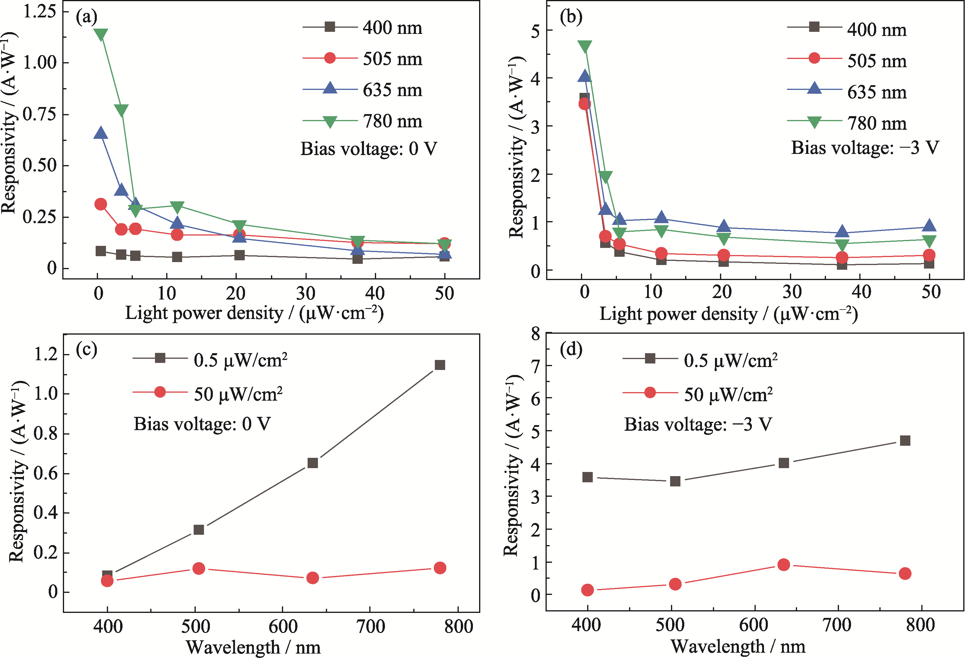
Fig. 5 Responsivity of the CuI/Si photodiode as a function of light power density and responsivity under specific light intensity (a) 0 V bias applied; (b) -3 V bias applied; (c) 0 V bias applied under specific light intensity; (d) -3 V bias applied under specific light intensity
| Wavelength/nm | Bias voltage/V | Responsivity (Weak/strong light)/(A·W-1) | D* (Weak/strong light)/ (×1013, Jones) | EQE (Weak/strong light)/% |
|---|---|---|---|---|
| 400 | 0 | 0.08/0.06 | 0.363/0.241 | 26/17 |
| -3 | 3.58/0.15 | 15.4/0.669 | 1109/48 | |
| 505 | 0 | 0.31/0.14 | 1.35/0.618 | 77/35 |
| -3 | 3.46/0.30 | 14.9/1.31 | 849/74 | |
| 635 | 0 | 0.65/0.13 | 2.82/0.561 | 127/25 |
| -3 | 4.00/0.90 | 17.3/3.88 | 782/175 | |
| 780 | 0 | 1.15/0.20 | 4.94/0.844 | 182/31 |
| -3 | 4.70/0.67 | 20.3/2.92 | 747/107 |
Table 1 Device parameters of the CuI/Si photodiodes
| Wavelength/nm | Bias voltage/V | Responsivity (Weak/strong light)/(A·W-1) | D* (Weak/strong light)/ (×1013, Jones) | EQE (Weak/strong light)/% |
|---|---|---|---|---|
| 400 | 0 | 0.08/0.06 | 0.363/0.241 | 26/17 |
| -3 | 3.58/0.15 | 15.4/0.669 | 1109/48 | |
| 505 | 0 | 0.31/0.14 | 1.35/0.618 | 77/35 |
| -3 | 3.46/0.30 | 14.9/1.31 | 849/74 | |
| 635 | 0 | 0.65/0.13 | 2.82/0.561 | 127/25 |
| -3 | 4.00/0.90 | 17.3/3.88 | 782/175 | |
| 780 | 0 | 1.15/0.20 | 4.94/0.844 | 182/31 |
| -3 | 4.70/0.67 | 20.3/2.92 | 747/107 |
| Diode structure | Wavelength/ nm | Power density/ (μW·cm−2) | Bias voltage/V | D*/Jones | Responsivity/ (A·W-1) | EQE/% | Ref. |
|---|---|---|---|---|---|---|---|
| SnSe/Si | 405 | 10 | -4 | 3.4×10¹¹ | 0.21 | - | [ |
| 405 | 300 | -4 | 3.0×10¹¹ | 0.18 | - | ||
| 650 | 10 | 0 | 1.1×10¹¹ | 0.20 | - | ||
| 650 | 300 | 0 | 1.0×10¹¹ | 0.17 | - | ||
| MoS2/Si | 514 | 3 | -2 | 2.2×10¹¹ | 1.25 | - | [ |
| 514 | 80 | -2 | 8.0×10¹¹ | 0.90 | - | ||
| Graphene-Si | 730 | 10 | -2 | 2.1×10⁸ | 0.35 | - | [ |
| Si/ZnO | 550 | - | -2 | - | 0.37 | - | [ |
| ZnTe-TeO2/Si | 350 | - | 0 | 4.0×10¹² | 0.03 | - | [ |
| 850 | - | 0 | 1.4×10¹³ | 0.08 | - | ||
| CuI/Si | 400 | 0.5 | -3 | 1.54×10¹⁴ | 3.58 | 1109 | This work |
| 400 | 50 | -3 | 6.69×10¹² | 0.15 | 48 | ||
| 780 | 0.5 | 0 | 4.94×10¹³ | 1.15 | 182 | ||
| 780 | 50 | 0 | 8.44×10¹² | 0.20 | 31 |
Table 2 Summarization of photoelectric properties in Si-based photodiodes
| Diode structure | Wavelength/ nm | Power density/ (μW·cm−2) | Bias voltage/V | D*/Jones | Responsivity/ (A·W-1) | EQE/% | Ref. |
|---|---|---|---|---|---|---|---|
| SnSe/Si | 405 | 10 | -4 | 3.4×10¹¹ | 0.21 | - | [ |
| 405 | 300 | -4 | 3.0×10¹¹ | 0.18 | - | ||
| 650 | 10 | 0 | 1.1×10¹¹ | 0.20 | - | ||
| 650 | 300 | 0 | 1.0×10¹¹ | 0.17 | - | ||
| MoS2/Si | 514 | 3 | -2 | 2.2×10¹¹ | 1.25 | - | [ |
| 514 | 80 | -2 | 8.0×10¹¹ | 0.90 | - | ||
| Graphene-Si | 730 | 10 | -2 | 2.1×10⁸ | 0.35 | - | [ |
| Si/ZnO | 550 | - | -2 | - | 0.37 | - | [ |
| ZnTe-TeO2/Si | 350 | - | 0 | 4.0×10¹² | 0.03 | - | [ |
| 850 | - | 0 | 1.4×10¹³ | 0.08 | - | ||
| CuI/Si | 400 | 0.5 | -3 | 1.54×10¹⁴ | 3.58 | 1109 | This work |
| 400 | 50 | -3 | 6.69×10¹² | 0.15 | 48 | ||
| 780 | 0.5 | 0 | 4.94×10¹³ | 1.15 | 182 | ||
| 780 | 50 | 0 | 8.44×10¹² | 0.20 | 31 |
| [1] |
YU X, MARKS T, FACCHETTI A. Metal oxides for optoelectronic applications. Nature Materials, 2016, 15: 383.
DOI PMID |
| [2] | WOODS-ROBINSON R, HAN Y B, ZHANG H Y, et al. Wide band gap chalcogenide semiconductors. Chemical Reviews, 2020, 120(9): 4007. |
| [3] | ZHANG C, NICOLOSI V. Graphene and MXene-based transparent conductive electrodes and supercapacitors. Energy Storage Materials, 2019, 16: 102. |
| [4] |
FANG H, ZHAO Z, WU W, et al. Progress in flexible electrochromic devices. Journal of Inorganic Materials, 2021, 36(2): 140.
DOI |
| [5] | LIU H, LI H, TAO J, et al. Single crystalline transparent conducting F, Al, and Ga Co-doped ZnO thin films with high photoelectrical performance. ACS Applied Materials & Interfaces, 2023, 15(18): 22195. |
| [6] | YUTAKA F, TARO H, YUKIO Y, et al. A transparent metal: Nb-doped anatase TiO2. Applied Physics Letters, 2005, 86(25): 252101. |
| [7] | WILLIS J, SCANLON D. Latest directions in p-type transparent conductor design. Journal of Materials Chemistry C, 2021, 9: 11995. |
| [8] | YANG C, KNEISS M, SCHEIN F L, et al. Room-temperature domain-epitaxy of copper iodide thin films for transparent CuI/ZnO heterojunctions with high rectification ratios larger than 109. Scientific Reports, 2016, 6: 21937. |
| [9] |
LI Z, HE J, LV X, et al. Optoelectronic properties and ultrafast carrier dynamics of copper iodide thin films. Nature Communications, 2022, 13: 6346.
DOI PMID |
| [10] | YANG C, MAX K, MICHAEL L, et al. Room-temperature synthesized copper iodide thin film as degenerate p-type transparent conductor with a boosted figure of merit. Applied Physical Sciences, 2016, 113(46): 12929. |
| [11] | MARIUS G, FRIEDRICH S, MICHAEL L, et al. Cuprous iodide-a p-type transparent semiconductor: history and novel applications. Physica Status Solidi A, 2013, 210(9): 1671. |
| [12] | TANAKA T, KEISHI K, MASATAKA H. Transparent, conductive CuI films prepared by rf-dc coupled magnetron sputtering. Thin Solid Films, 1996, 281: 179. |
| [13] | KIM D, NAKAYAM M, KOJIM O, et al. Thermal-strain-induced splitting of heavy and light-hole exciton energies in CuI thin films grown by vacuum evaporation. Physical Review B, 1999, 60(19): 13879. |
| [14] | ZI M, LI J, ZHANG Z, et al. Effect of deposition temperature on transparent conductive properties of γ-CuI film prepared by vacuum thermal evaporation. Phys. Status Solidi, 2015, 212: 1466. |
| [15] | KANG H, LIU R, CHEN K, et al. Electrodeposition and optical properties of highly oriented γ-CuI thin films. Electrochim Acta, 2010, 55(27): 8121. |
| [16] | YAMADA N, KONDO Y, INO R. Low-temperature fabrication and performance of polycrystalline CuI films as transparent p-type semiconductors. Physica Status Solidi, 2019, 216(5): 1700782. |
| [17] | STORM P, BAR M, BENNDORF G, et al. High mobility, highly transparent, smooth, p-type CuI thin films grown by pulsed laser deposition. APL Materials, 2020, 8(9): 091115. |
| [18] | YANG C, ROSE E, YU W, et al. Controllable growth of copper iodide for high-mobility thin films and self-assembled microcrystals. ACS Applied Electronic Materials, 2020, 2(11): 3627. |
| [19] | GENG F, WU Y, SPLITH D, et al. Amorphous transparent Cu(S,I) thin films with very high hole conductivity. Journal of Physical Chemistry Letters, 2023, 14(26): 6163. |
| [20] | GENG F, WANG L, STRALKA T, et al. (111)-oriented growth and acceptor doping of transparent conductive CuI:S thin films by spin coating and radio frequency-sputtering. Advanced Engineering Materials, 2023, 25(11): 2201666. |
| [21] |
YANG C, SOUCHAY D, KNEISS M, et al. Transparent flexible thermoelectric material based on non-toxic earth-abundant p-type copper iodide thin film. Nature Communications, 2017, 8: 16076.
DOI PMID |
| [22] | CHA J, JUNG D. Air-stable transparent silver iodide-copper iodide heterojunction diode. ACS Applied Materials Interfaces, 2017, 9(50): 43807. |
| [23] | NAOOMI Y, YUUMI K, XIANG C, et al. Visible-blind wide-dynamic-range fast-response self-powered ultraviolet photodetector based on CuI/In-Ga-Zn-O heterojunction. Applied Materials Today, 2019, 15: 153. |
| [24] | AKSHAI S, NANDAKUMAR A, RAMESH R, et al. Self-powered UV photodetectors based on heterojunctions composed of ZnO nanorods coated with thin films of ZnS and CuI. ACS Applied Nano Materials, 2023, 6(10): 8529. |
| [25] | ZHANG Y, LI S, YANG W, et al. Millimeter-sized single-crystal CsPbrB3/CuI heterojunction for high-performance self-powered photodetector. Journal of Physical Chemistry Letters, 2019, 10(10): 2400. |
| [26] | WANG Y, CHUANG C. Solution processed CuI/n-Si junction device annealed with and without iodine steam for ultraviolet photodetector applications. Journal of Materials Science, 2018, 29(21): 18622. |
| [27] | LI W, SHI W. Growth habit and habit variation of γ-CuI crystallites under hydrothermal conditions. Crystal Research & Technology, 2002, 37(10): 1041. |
| [28] | ALIVOV Y, ÖZGÜR Ü, DOĞAN S, et al. Photoresponse of n-ZnO/p-SiC heterojunction diodes grown by plasma-assisted molecular-beam epitaxy. Applied Physics Letters, 2005, 86(24): 241108. |
| [29] | LEE M, SEO S, KIM D, et al. A low-temperature grown oxide diode as a new switch element for high-density, nonvolatile memories. Advanced Materials, 2007, 19(1): 73. |
| [30] | BRÖTZMANN M, VETTER U, HOFSÄSS H. BN/ZnO heterojunction diodes with apparently giant ideality factors. Journal of Applied Physics, 2009, 106(6): 063704. |
| [31] | SCHENK A, KRUMBEIN U. Coupled defect level recombination: theory and application to anomalous diode characteristics. Journal of Applied Physics, 1995, 78(5): 3185. |
| [32] | YASUHISA O, YOSHIAKI M, SHINGO S, et al. Revisiting the role of trap-assisted-tunneling process on current-voltage characteristics in tunnel field-effect transistors. Journal of Applied Physics, 2018, 123(16): 161549. |
| [33] | TALIN A, ALEC, LEONARD F, SWART B, et al. Unusually strong space-charge-limited current in thin wires. Physical Review Letters, 2008, 101: 076802. |
| [34] | YU W, BENNDORF G, JIANG Y, et al. Control of optical absorption and emission of sputtered copper iodide thin films. Physica Status Solidi (RRL)-Rapid Research Letters, 2020, 15(1): 2000431. |
| [35] |
YANG Y, SHAO Y, LI B, et al. Enhanced band-edge luminescence of CuI thin film by Cl-doping. Journal of Inorganic Materials, 2023, 38(6): 687.
DOI |
| [36] | LUO F, ZHOU H, LIU Y, et al. High-performance self-driven SnSe/Si heterojunction photovoltaic photodetector. Chemosensors, 2023, 11: 406. |
| [37] | MUKHERJEE S, MAITI R, KATIYAR A, et al. Novel colloidal MoS2 quantum dot heterojunctions on silicon platforms for multifunctional optoelectronic devices. Scientific Reports, 2016, 6: 29016. |
| [38] | AN X, LIU F, JUNG Y, et al. Tunable graphenesilicon heterojunctions for ultrasensitive photodetection. Nano Letters, 2013, 13(3): 909. |
| [39] | LIM S, UM D, HA M, et al. Broadband omnidirectional light detection in flexible and hierarchical ZnO/Si heterojunction photodiodes. Nano Research, 2017, 10: 22. |
| [40] | SAHATIYA P, REDDY C, BADHULIKA S. Discretely distributed 1D V2O5 nanowires over 2D MoS2 nanoflakes for an enhanced broadband flexible photodetector covering the ultraviolet to near infrared region. Journal of Materials Chemistry C, 2017, 5(48): 12728. |
| [41] | YIN W, YANG J, ZHAO K, et al. High responsivity and external quantum efficiency photodetectors based on solution-processed Ni-doped CuO films. ACS Applied Materials & Interfaces, 2020, 12(10): 11797. |
| [42] | HONG Q, CAO Y, HU J, et al. Self-powered ultrafast broadband photodetector based on p-n heterojunctions of CuO/Si nanowire array. ACS Applied Materials & Interfaces, 2014, 6(23): 20887. |
| [43] | SONG Z, LIU Y, WANG Q, et al. Self-powered photodetectors based on a ZnTe-TeO2 composite/Si heterojunction with ultra- broadband and high responsivity. Journal of Materials Science, 2018, 53: 7562. |
| [1] | HONG Enliu, TU Xinchen, LI Ziqing, FANG Xiaosheng. Two-dimensional Perovskite Single Crystal Nanosheets: Floating Growth and Optoelectronic Performance [J]. Journal of Inorganic Materials, 2026, 41(6): 787-794. |
| [2] | LI Zexi, LU Wenjie, WANG Chao, ZHANG Lu, LI Shuti, GAO Fangliang. Two-dimensional GaN: Preparation Based on Liquid Metal Gallium and Photoelectric Properties [J]. Journal of Inorganic Materials, 2026, 41(3): 377-384. |
| [3] | ZHU Jianhua, YANG Xin, RU Lingjie. 2D/2D Coupled ZnIn2S4/TiO2 Heterojunction and Its Enhanced Photocatalytic Reduction of CO2 [J]. Journal of Inorganic Materials, 2026, 41(2): 177-185. |
| [4] | JIA Xianghua, ZHANG Huixia, LIU Yanfeng, ZUO Guihong. Cu2O/Cu Hollow Spherical Heterojunction Photocatalysts Prepared by Wet Chemical Approach [J]. Journal of Inorganic Materials, 2025, 40(4): 397-404. |
| [5] | YE Maosen, WANG Yao, XU Bing, WANG Kangkang, ZHANG Shengnan, FENG Jianqing. II/Z-type Bi2MoO6/Ag2O/Bi2O3 Heterojunction for Photocatalytic Degradation of Tetracycline under Visible Light Irradiation [J]. Journal of Inorganic Materials, 2024, 39(3): 321-329. |
| [6] | LI La, SHEN Guozhen. 2D MXenes Based Flexible Photodetectors: Progress and Prospects [J]. Journal of Inorganic Materials, 2024, 39(2): 186-194. |
| [7] | CHAO Shaofei, XUE Yanhui, WU Qiong, WU Fufa, MUHAMMAD Sufyan Javed, ZHANG Wei. Efficient Potassium Storage through Ti-O-H-O Electron Fast Track of MXene Heterojunction [J]. Journal of Inorganic Materials, 2024, 39(11): 1212-1220. |
| [8] | ZHANG Shumin, XI Xiaowen, SUN Lei, SUN Ping, WANG Deqiang, WEI Jie. Sonodynamic and Enzyme-like Activities of Niobium-based Coatings: Antimicrobial, Cell Proliferation and Cell Differentiation [J]. Journal of Inorganic Materials, 2024, 39(10): 1125-1134. |
| [9] | HU Ying, LI Ziqing, FANG Xiaosheng. Solution-prepared AgBi2I7 Thin Films and Their Photodetecting Properties [J]. Journal of Inorganic Materials, 2023, 38(9): 1055-1061. |
| [10] | CAI Kai, JIN Zhiwen. Photodetector Based on Two-dimensional Perovskite (PEA)2PbI4 [J]. Journal of Inorganic Materials, 2023, 38(9): 1069-1075. |
| [11] | LI Yuejun, CAO Tieping, SUN Dawei. Bi4O5Br2/CeO2 Composite with S-scheme Heterojunction: Construction and CO2 Reduction Performance [J]. Journal of Inorganic Materials, 2023, 38(8): 963-970. |
| [12] | TUERHONG Munire, ZHAO Honggang, MA Yuhua, QI Xianhui, LI Yuchen, YAN Chenxiang, LI Jiawen, CHEN Ping. Construction and Photocatalytic Activity of Monoclinic Tungsten Oxide/Red Phosphorus Step-scheme Heterojunction [J]. Journal of Inorganic Materials, 2023, 38(6): 701-707. |
| [13] | WU Lin, HU Minglei, WANG Liping, HUANG Shaomeng, ZHOU Xiangyuan. Preparation of TiHAP@g-C3N4 Heterojunction and Photocatalytic Degradation of Methyl Orange [J]. Journal of Inorganic Materials, 2023, 38(5): 503-510. |
| [14] | MA Rundong, GUO Xiong, SHI Kaixuan, AN Shengli, WANG Ruifen, GUO Ruihua. S-type Heterojunction of MOS2/g-C3N4: Construction and Photocatalysis [J]. Journal of Inorganic Materials, 2023, 38(10): 1176-1182. |
| [15] | MA Xinquan, LI Xibao, CHEN Zhi, FENG Zhijun, HUANG Juntong. BiOBr/ZnMoO4 Step-scheme Heterojunction: Construction and Photocatalytic Degradation Properties [J]. Journal of Inorganic Materials, 2023, 38(1): 62-70. |
| Viewed | ||||||
|
Full text |
|
|||||
|
Abstract |
|
|||||