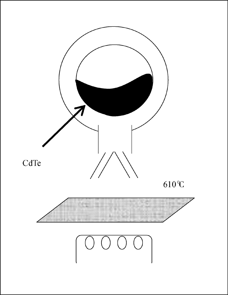
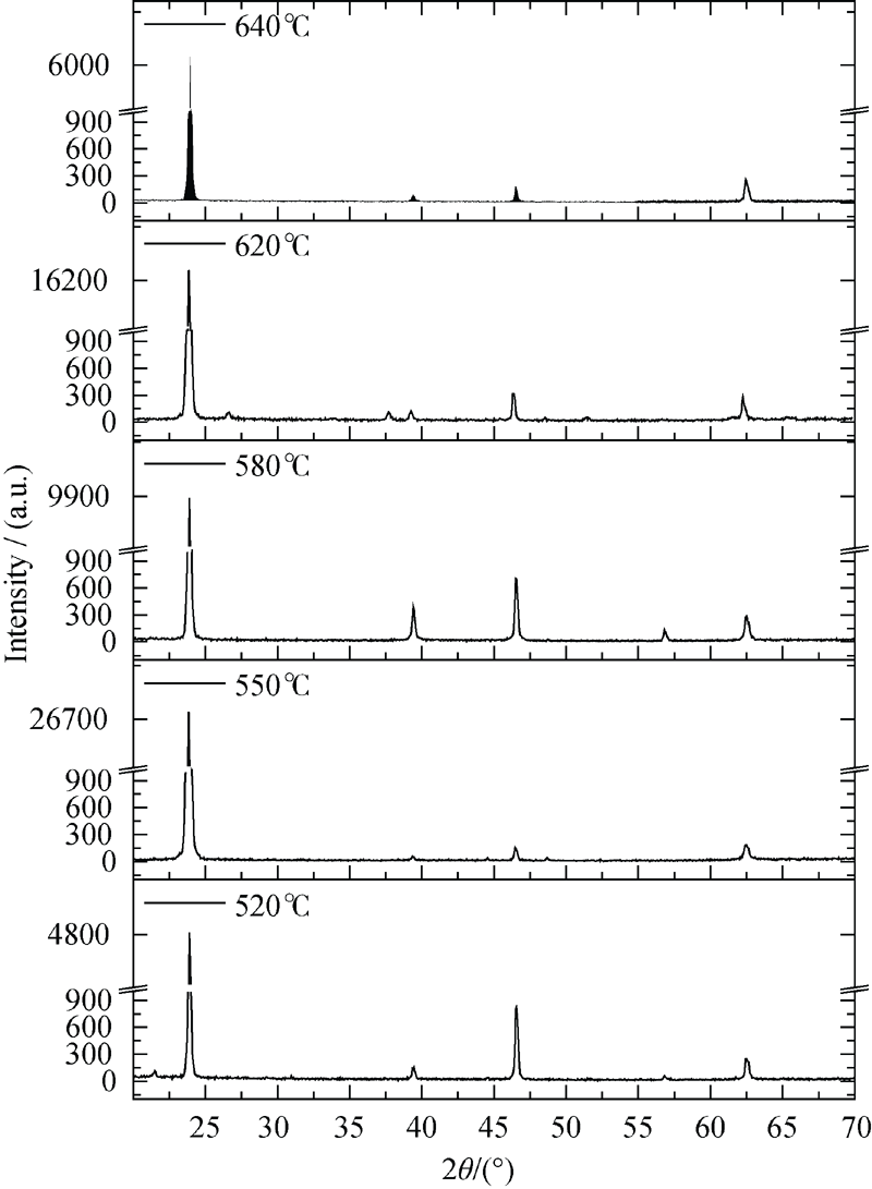
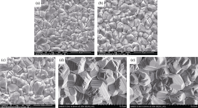
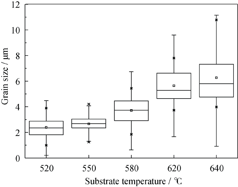
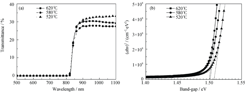
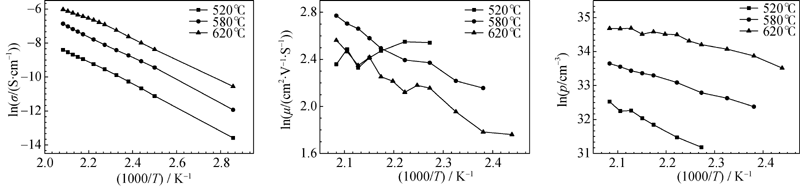
Journal of Inorganic Materials ›› 2016, Vol. 31 ›› Issue (2): 141-147.DOI: 10.15541/jim20150310
• Orginal Article • Previous Articles Next Articles
CAO Sheng, WU Li-Li, FENG Liang-Huan, WANG Wen-Wu, ZHANG Jing-Quan, YU Xiao-Qi, LI Xin-Xin, LI Wei, LI Bing
Received:
2015-07-06
Revised:
2015-08-30
Published:
2016-02-20
Online:
2016-01-15
About author:
CAO Sheng. E-mail: caosheng0819@163.com
Supported by:
CLC Number:
CAO Sheng, WU Li-Li, FENG Liang-Huan, WANG Wen-Wu, ZHANG Jing-Quan, YU Xiao-Qi, LI Xin-Xin, LI Wei, LI Bing. Effect of Substrate Temperature on CdTe Thin Film Property and Solar Cell Performance[J]. Journal of Inorganic Materials, 2016, 31(2): 141-147.
Substrate temperature/℃ | Ci | σ | ||||
---|---|---|---|---|---|---|
(111) | (220) | (311) | (440) | (331) | ||
520 | 2.98 | 0.10 | 0.96 | 0.27 | 0.67 | 1.04 |
550 | 4.79 | 0.01 | 0.05 | 0.01 | 0.13 | 1.89 |
580 | 3.44 | 0.14 | 0.43 | 0.31 | 0.66 | 1.23 |
620 | 4.45 | 0.03 | 0.15 | 0.06 | 0.36 | 1.72 |
640 | 3.96 | 0.06 | 0.22 | 0.11 | 0.65 | 1.49 |
Table 1 Texture coefficient Ci and standard deviation σ of CdTe films for different substrate temperatures
Substrate temperature/℃ | Ci | σ | ||||
---|---|---|---|---|---|---|
(111) | (220) | (311) | (440) | (331) | ||
520 | 2.98 | 0.10 | 0.96 | 0.27 | 0.67 | 1.04 |
550 | 4.79 | 0.01 | 0.05 | 0.01 | 0.13 | 1.89 |
580 | 3.44 | 0.14 | 0.43 | 0.31 | 0.66 | 1.23 |
620 | 4.45 | 0.03 | 0.15 | 0.06 | 0.36 | 1.72 |
640 | 3.96 | 0.06 | 0.22 | 0.11 | 0.65 | 1.49 |
Substrate temperature | Electrical parameters (300 K) | Activation energy | |||||
---|---|---|---|---|---|---|---|
ρ/ (Ω·cm) | Rsh/ (Ω·□-1) | P /cm-3 | μ/ (cm2·V-1·s-1) | Ea /eV | Eap /eV | Eaμ /eV | |
520℃ | 1.76×10⁶ | 3.84×10⁹ | 1.93×10¹⁰ | - | 0.576 | 0.608 | - |
580℃ | 2.94×10⁶ | 6.75×10⁹ | 1.96×10¹² | 1.171 | 0.554 | 0.369 | 0.178 |
620℃ | 5.84×10⁵ | 1.34×10⁹ | 2.36×10¹³ | 0.756 | 0.509 | 0.277 | 0.192 |
Table 2 Electrical parameters of CdTe films deposited at different substrate temperatures
Substrate temperature | Electrical parameters (300 K) | Activation energy | |||||
---|---|---|---|---|---|---|---|
ρ/ (Ω·cm) | Rsh/ (Ω·□-1) | P /cm-3 | μ/ (cm2·V-1·s-1) | Ea /eV | Eap /eV | Eaμ /eV | |
520℃ | 1.76×10⁶ | 3.84×10⁹ | 1.93×10¹⁰ | - | 0.576 | 0.608 | - |
580℃ | 2.94×10⁶ | 6.75×10⁹ | 1.96×10¹² | 1.171 | 0.554 | 0.369 | 0.178 |
620℃ | 5.84×10⁵ | 1.34×10⁹ | 2.36×10¹³ | 0.756 | 0.509 | 0.277 | 0.192 |
[1] | HENRY C H.Limiting efficiencies of ideal single and multiple energy gap terrestrial solar cells.Journal of Applied Physics, 1980, 51(8): 4494-4500. |
[2] | GORJI N E.Electrical and optical characterization of RF-sputtered CdTe thin films.IEEE Transactions on Device and Materials Reliability, 2014, 14(4): 983-988. |
[3] | FEREKIDES C S, MARINSKIY D, VISWANATHAN V, et al.High efficiency CSS CdTe solar cells.Thin Solid Films, 2000, (361/362): 520-526. |
[4] | ROSE D, POWELL R, JAYAMAHA U, et al.R&D of CdTe-absorber Photovoltaic Cells, Modules, and Manufacturing Equipment: Plan and Progress to 100 MW/yr. IEEE, 2000: 428-431. |
[5] | SHARMA R K, SINGH G, RASTOGI A C.Pulsed electrodeposition of CdTe thin films: effect of pulse parameters over structure, stoichiometry and optical absorption.Solar Energy Materials and Solar Cells, 2003, 82(1/2): 201-215. |
[6] | NAKAYAMA N, MATSUMOTO H, NAKANO A, et al.Screen printed thin-film CdS-CdTe solar-cell.Japanese Journal of Applied Physics. 1980, 19(4): 703-712. |
[7] | GREEN M A, EMERY K, HISHIKAWA Y, et al.Solar cell efficiency tables (version 42).Progress in Photovoltaics: Research and Applications, 2013, 21(5): 827-837. |
[8] | GREEN M A, EMERY K, HISHIKAWA Y, et al.Solar cell efficiency tables (Version 45).Progress in Photovoltaics: Research and Applications. 2015, 23(1): 1-9. |
[9] | MCCANDLESS B E, BIRKMIRE R W, BUCHANAN W A.Vapor Transport Deposition of Cadmium Telluride Films.IEEE, 2002: 547-550. |
[10] | KESTNER J M, MCELVAIN S, KELLY S, et al.An experimental and modeling analysis of vapor transport deposition of cadmium telluride.Solar Energy Materials and Solar Cells, 2004, 83(1): 55-65. |
[11] | YANG K, CHA B, HEO D, et al.Vapor transport deposition of large-area polycrystalline CdTe for radiation image sensor application.Physica Status Solidi (c), 2014, 11(7/8): 1341-1344. |
[12] | ZHENG J, LEI Z, ZHANG J, et al.Spectral analysis of the effect of annealing on CdTe polycrystalline film.Spectroscopy and Spectral Analysis, 2010, 30(3): 753-756. |
[13] | MAJOR J D, BOWEN L, TREHARNE R, et al.Assessment of photovoltaic junction position using combined focused ion beam and electron beam-induced current analysis of close space sublimation deposited CdTe solar cells.Progress in Photovoltaics: Research and Applications, 2014, 22(10): 1096-1104. |
[1] | XIAO Zichen, HE Shihao, QIU Chengyuan, DENG Pan, ZHANG Wei, DAI Weideren, GOU Yanzhuo, LI Jinhua, YOU Jun, WANG Xianbao, LIN Liangyou. Nanofiber-modified Electron Transport Layer for Perovskite Solar Cells [J]. Journal of Inorganic Materials, 2024, 39(7): 828-834. |
[2] | CHEN Yu, LIN Puan, CAI Bing, ZHANG Wenhua. Research Progress of Inorganic Hole Transport Materials in Perovskite Solar Cells [J]. Journal of Inorganic Materials, 2023, 38(9): 991-1004. |
[3] | ZHANG Lun, LYU Mei, ZHU Jun. Research Progress of Cs2AgBiBr6 Perovskite Solar Cell [J]. Journal of Inorganic Materials, 2023, 38(9): 1044-1054. |
[4] | HE Xu, REN Sheng-Qiang, LI Chun-Xiu, WU Li-Li, ZHANG Jing-Quan, DU Zheng. Zn1-xMgxO: Band Structure and Simulation as Window Layer for CdTe Solar Cell by SCAPS Software [J]. Journal of Inorganic Materials, 2018, 33(6): 635-640. |
[5] | HUANG Yao-Qin, ZHENG Guo-Yuan, MO Shu-Yi, HE Li-Qiu, WANG Dong-Sheng, LONG Fei. Liquid-assisted Hot-pressed Sintering of Cu(In, Ga)Se2 Targets [J]. Journal of Inorganic Materials, 2016, 31(10): 1141-1146. |
[6] | XIE Shou-Dong, WANG Gang, CHEN Hui-Yuan, LIN Hong, YAN Zhi-Nan, ZHANG Hui. Lycium ruthenicum Murray and Graphene Nanoplates for Dye Sensitized Solar Cell [J]. Journal of Inorganic Materials, 2016, 31(10): 1117-1122. |
[7] | XU Ya-Xin, XIONG Jie, XIA Yu-Dong, ZHANG Fei, XUE Yan, TAO Bo-Wan. [J]. Journal of Inorganic Materials, 2013, 28(5): 491-496. |
[8] | YANG Jia-Yi, GAO Jing-Jing, WANG Wen-Wu, ZENG Guang-Gen, LI Wei, FENG Liang-Huan, ZHANG Jing-Quan, WU Li-Li, LI Bing. Optoelectrical Properties and Back Contact Characteristic of VSe2 Thin Films [J]. Journal of Inorganic Materials, 2013, 28(3): 312-316. |
[9] | YU Fang-Li, BAI YU, QIN Yi, YUE Dong, LUO Cai-Jun, YANG Jian-Feng. Influence of Substrate Temperature on the Morphology, Composition and Growth Rate of SiC Films Deposited by PECVD [J]. Journal of Inorganic Materials, 2013, 28(2): 201-206. |
[10] | CUI Xu-Mei, ZUO Cheng-Yang, LAN De-Jun, WANG Jun. Preparation and Electrical Properties of TiO2/SnO2 Nanocrystalline Films [J]. Journal of Inorganic Materials, 2013, 28(11): 1233-1236. |
[11] | HUANG Shuai, LI Chen-Hui, SUN Yi-Hua, KE Wen-Ming. Influence of the Substrate Temperature on the Properties of Nb-doped TiO2 Films Deposited by DC Magnetron Sputtering [J]. Journal of Inorganic Materials, 2012, 27(1): 64-68. |
[12] | ZHU Jia-Qi,LU Jia,TIAN Gui,TAN Man-Lin,GENG Da. Using Boron Doped Amorphous Diamond Films as Window Layer of Amorphous Silicon Solar Cells [J]. Journal of Inorganic Materials, 2008, 23(5): 1064-1066. |
[13] | WANG Chuan-Bin,TU Rong,GOTO Takashi,SHEN Qiang,ZHANG Lian-Meng. Preparation of b-axis Oriented BaTi2O5 Thin Films by Pulsed Laser Deposition [J]. Journal of Inorganic Materials, 2008, 23(3): 553-556. |
[14] | LIU Jin-Feng,LIU Zhong-Liang,WU Yu-Yu,XU Peng-Shou,TANG Hong-Gao. Effects of Substrate Temperature on Heteroepitaxial Growth of 3C-SiC Thin Films by MBE on Si(111) Substrate [J]. Journal of Inorganic Materials, 2007, 22(4): 720-724. |
[15] | CHEN Zhi-Qiang,FANG Guo-Jia,LI Chun,SHENG Su,ZHAO Xing-Zhong. Fabrication and Properties of Pulsed Laser Deposited Wide Band-gap Zn0.9Mg0.1O:Ga Conducting Films [J]. Journal of Inorganic Materials, 2006, 21(3): 707-712. |
Viewed | ||||||
Full text |
|
|||||
Abstract |
|
|||||