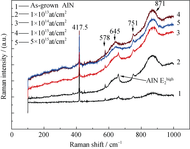
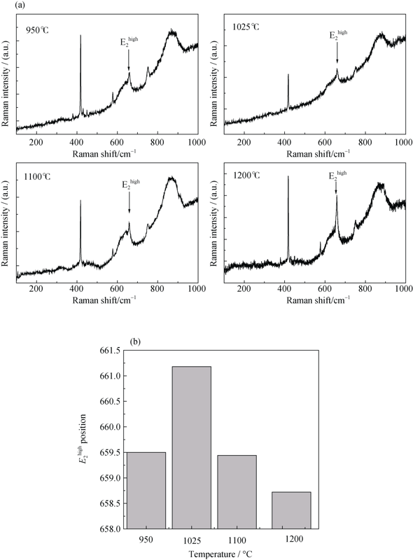
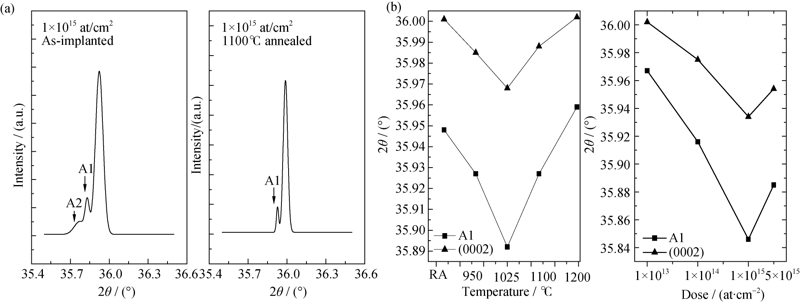
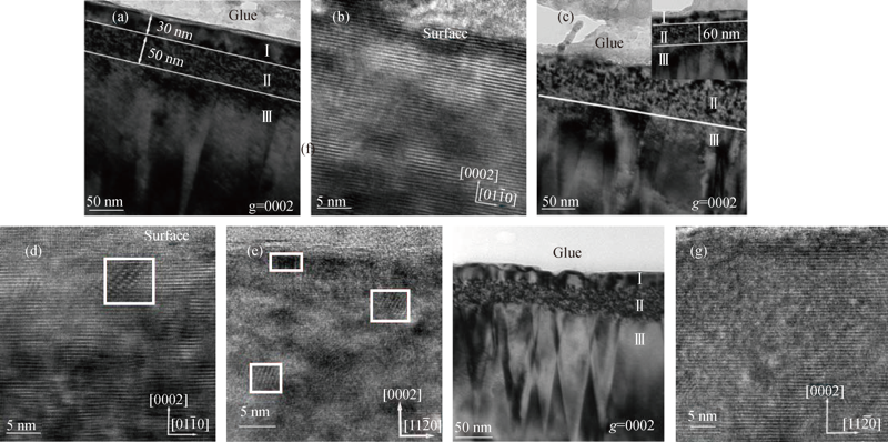
| [1] |
HÖMMERICH U, NYEIN E E, LEE D S, et al. Photoluminescence studies of rare earth (Er, Eu, Tm) in situ doped GaN. Appl. Phys. Lett., 2003, 105(3): 91-96.
|
| [2] |
RUTERANA P, LACROIX B, LORENZ K, et al. A mechanism for damage formation in GaN during rare earth implantation at medium range energy and room temperature. Journal of Applied Physics, 2011, 109(1): 013506.
|
| [3] |
WANG C M, JIANG W, WEBER W J.Defect clustering in GaN irradiated with O+ ions.Journal of Materials Research, 2002, 17(11): 2945-2952.
|
| [4] |
LECLERC S, LACROIX B, DECLEMY A, et al. Mechanisms of damage formation in Eu-implanted AlN. Journal of Applied Physics, 2012, 112(7): 073525.
|
| [5] |
PIERRE RUTERANA, MARIE-PIERRE CHAUVANT, KATHARINA LORENZ. Mechanisms of damage formation during rare earth ion implantation in nitride semiconductors. Japanese Journal of Applied Physics, 2013, 52(11): UNSP 11NH02.
|
| [6] |
SOARES M J, LEITÃO J P, SLIVA,et al. Structural and optical properties of Er implanted AlN thin films: green and infrared photoluminescence at room temperature. Optical Materials, 2011, 33(7): 1055-1058.
|
| [7] |
LORENZ K E, ALVES T, MONTEIRO, et al. Optical doping of AlN by rare earth implantation. Nuclear Instruments and Methods in Physics Research B, 2006, 224(1/2): 307-310.
|
| [8] |
LU F, RIZZI A, CARIUS R.Lattice disorder and photoluminescence of Er-implanted AlN crystalline films.Chinese Physcics Letter, 2002, 19(12): 1844-1847.
|
| [9] |
DAVYDOV V Y, AVERKIEV N S, GONCHARUK, et al. Raman and photoluminescence studies of biaxial strain in GaN epitaxial layers grown on 6H-SiC. Journal of Applied Physics, 1998, 82(10): 5097-5102.
|
| [10] |
KUNERT H W, MACHATINE A G J, HOFFMANN A, et al. Phonons in sapphire Al2O3 substrate for ZnO and GaN. Material Science and Engineering: C, 2007, 27(5-8): 1222-1226.
|
| [11] |
KALLEL T, DAMMAK M, WANG J.Raman characterization and stress analysis of AlN: Er3+ epilayers grown on sapphire and silicon substrates.Materials Science and Engineering B, 2014, 187: 46-52.
|
| [12] |
DADWAL RU, SCHOLZ M, REICHE P, et al. Effect of implantation temperature on the blistering behavior of hydrogen implanted GaN. Appl. Phys. A, 2013, 112(2): 451-456.
|
| [13] |
HUSNAIN G, YAO SHU-DE, ISHAQ AHMAD.Structural and magnetic impact of Cr+-implantation into GaN thin film.Solid State Science, 2012, 14(6): 735-738.
|
| [14] |
KUCHEYEV S O, WILLIAMS J S, JAGADISH C, et al. Damage buildup in GaN under ion bombardment. Phys. Rev. B, 2000, 62(11): 7510-7522.
|
| [15] |
KUCHEYEV S O, WILLIAMS J S, PEARTON S J.Ion implantation into GaN.Materials Science and Engineering, 2011, 33(2/3): 51-107.
|
| [16] |
KATSIKINI M, PINAKIDOU F, VOUROUTZISA N, et al. NEXAFS and AFM characterization of Si implanted GaN. Nuclear Instruments and Methods in Physics Research B, 2003, 200: 120-125.
|
 ), MO Ya-Juan3, WANG Xiao-Dan3, ZENG Xiong-Hui1(