无机材料学报 ›› 2026, Vol. 41 ›› Issue (7): 993-1000.DOI: 10.15541/jim20250420 CSTR: 32189.14.10.15541/jim20250420
黄奎碎( ), 王珂馨, 罗万豪, 李飞, 葛一瑶, 高艺璇(), 陈克新
收稿日期:2025-10-26
修回日期:2026-01-15
出版日期:2026-07-20
网络出版日期:2026-02-06
通讯作者:
高艺璇, 副研究员. E-mail: gaoyixuan@ustb.edu.cn作者简介:黄奎碎(2001-), 女, 硕士研究生. E-mail: m202511244@xs.ustb.edu.cn
基金资助:
HUANG Kuisui(), WANG Kexin, LUO Wanhao, LI Fei, GE Yiyao, GAO Yixuan(), CHEN Kexin
Received:2025-10-26
Revised:2026-01-15
Published:2026-07-20
Online:2026-02-06
Contact:
GAO Yixuan, associate professor. E-mail: gaoyixuan@ustb.edu.cnAbout author:HUANG Kuisui (2001-), female, Master candidate. E-mail: m202511244@xs.ustb.edu.cn
Supported by:摘要:
二维SixCy材料因其独特的结构可调性与优异的物理化学性能成为材料科学领域的研究热点。其中, 二维Si2C6、Si6C12、Si12C20被理论预言是一类新型拓扑绝缘体材料, Si2C6与Si12C20是具有狄拉克锥的半金属材料, 而Si6C12是具有本征大能隙的高阶拓扑绝缘体材料。目前, 应力对二维SixCy (Si2C6、Si6C12、Si12C20)材料电子性质的调控作用尚待研究。本研究采用基于密度泛函理论(Density Functional Theory, DFT)的第一性原理方法探究应变对二维SixCy (Si2C6、Si6C12、Si12C20)材料电子性质的调控规律。计算结果表明, 在双轴拉伸断裂应变附近, Si2C6与Si12C20的狄拉克锥仍保持完整, 但较小的双轴压缩应变或单轴应变会破坏Si2C6与Si12C20狄拉克点处的简并性, 使得Si2C6和Si12C20从拓扑绝缘体转变为平庸的直接带隙半导体。此外, 双轴应变对高阶拓扑绝缘体Si6C12的带隙具有调控作用, 在0~4%的压缩应变下, Si6C12的带隙随着压缩应变的增大而减小; 在0~10%的拉伸应变下, 带隙随着拉伸应变的增大而增大。Si6C12的带隙对应变变化较为敏感, 有望应用在半导体器件中。在断裂应变附近, Si6C12的价带与导带交叉, 体系表现为金属性。在单轴应变下, 拉伸或压缩应变会导致Si6C12在Γ点处的能带发生退简并。此外, 通过经典分子动力学(Molecular Dynamics, MD)模拟探究Si2C6、Si6C12、Si12C20的力学性质, 发现这类材料的断裂强度随着C/Si比值的减小而降低。Si2C6、Si6C12、Si12C20的断裂应变在0.32~0.37之间, 高于单晶石墨烯和无缺陷六方氮化硼, 具有良好的延展性。本文数据集可在
中图分类号:
黄奎碎, 王珂馨, 罗万豪, 李飞, 葛一瑶, 高艺璇, 陈克新. 利用应力调控二维新型SixCy的电子性质[J]. 无机材料学报, 2026, 41(7): 993-1000.
HUANG Kuisui, WANG Kexin, LUO Wanhao, LI Fei, GE Yiyao, GAO Yixuan, CHEN Kexin. Regulation of Electronic Properties of Novel Two-dimensional SixCy under External Strain[J]. Journal of Inorganic Materials, 2026, 41(7): 993-1000.
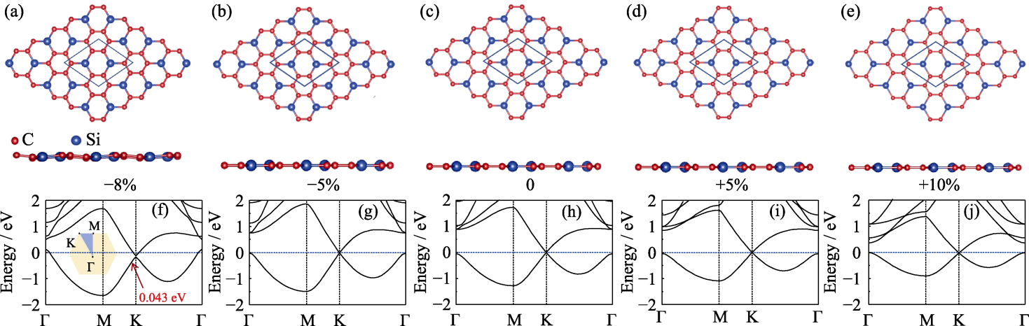
图1 二维Si2C6在-8%、-5%、0、+5%、+10%双轴应变下的(a~e)原子结构图和(f~j)能带结构图
Fig. 1 (a-e) Optimized atomic structures and (f-j) band structures of 2D Si2C6 under −8%, −5%, 0, +5%, and +10% biaxial strains
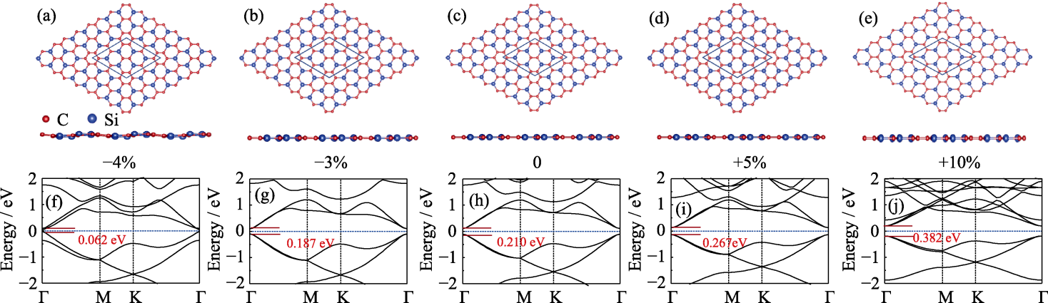
图2 二维Si6C12在−4%、−3%、0、+5%、+10%双轴应变下的(a~e)原子结构图和(f~j)能带结构图
Fig. 2 (a-e) Optimized atomic structures and (f-j) band structures of 2D Si6C12 under −4%, −3%, 0, +5%, and +10% biaxial strains
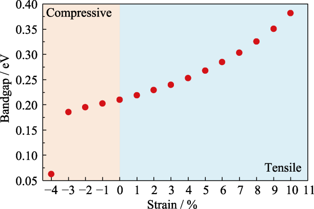
图3 Si6C12的带隙随应变的变化关系
Fig. 3 Bandgap evolution of Si6C12 with external strain
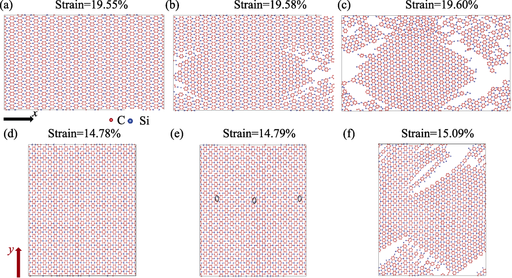
图4 Si2C6在MD模拟中分别沿(a~c) x、(d~f) y方向进行单轴拉伸的结构变化图
Fig. 4 Structural evolution of Si2C6 under uniaxial tensile along (a-c) x and (d-f) y directions in MD simulations
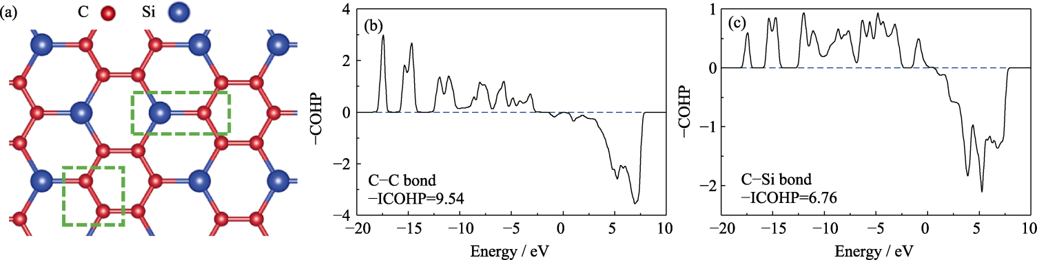
图5 Si2C6中C-C键和C-Si键的COHP
Fig. 5 COHP of C-C and C-Si bonds in Si2C6 (a) Schematic of selected C-C and C-Si bonds in Si2C6; (b, c) COHP of (b) C-C and (c) C-Si bonds
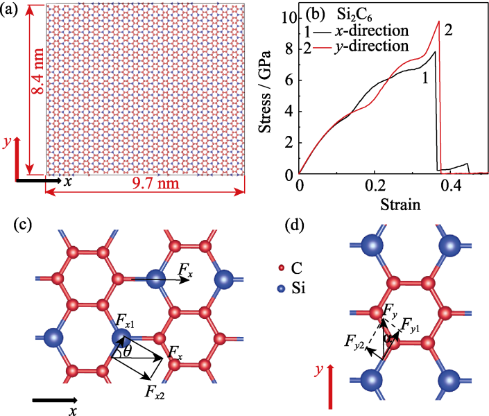
图6 Si2C6的拉伸曲线及受力分析图
Fig. 6 Tensile curves and stress analysis diagrams of Si2C6 (a) Atomic structure of Si2C6; (b) Stress-strain curves of Si2C6 stretched along x and y directions, respectively; (c, d) Force analysis diagrams for tensile loading along (c) x and (d) y directions
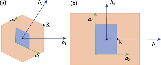
图S1 坐标变换示意图
Fig. S1 Schematic of coordinate transformation (a) Real space (blue) and reciprocal space (orange) of the hexagonal unit cell; (b) Real space (blue) and reciprocal space (orange) of the orthorhombic unit cell
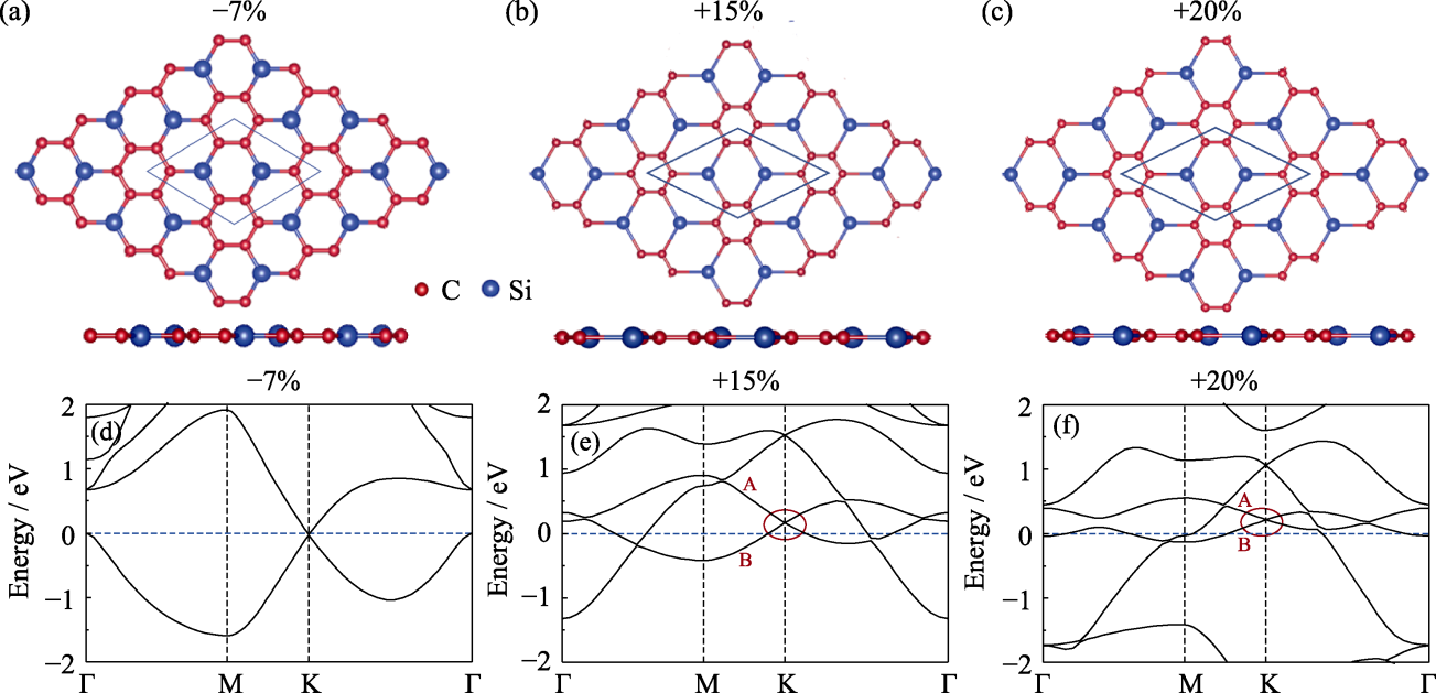
图S2 二维Si2C6在-7%、+15%、+20%双轴应变下的(a~c)原子结构图和(d~f)能带结构图
Fig. S2 (a-c) Optimized atomic structures and (d-f) band structures of 2D Si2C6 under -7%, +15% and +20% biaxial strains
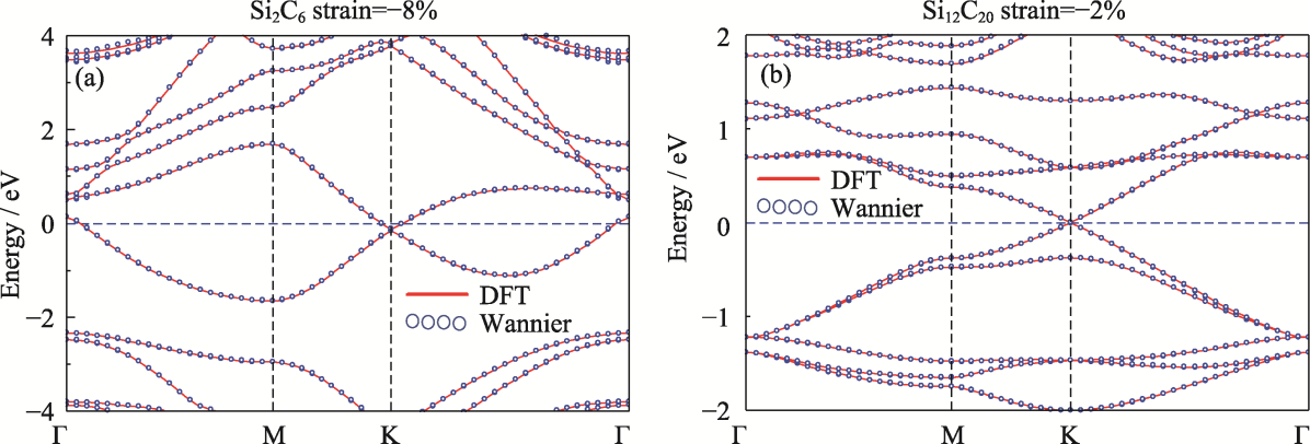
图S3 (a) Si2C6在-8%双轴应变、(b) Si12C20在-2%双轴应变下第一性原理计算的能带结构(红线)与Wannier能带结构(蓝圈)
Fig. S3 Band structures calculated by first-principles (red lines) and Wannier (blue circles) for (a) Si2C6 at -8% biaxial strain and (b) Si12C20 at -2% biaxial strain
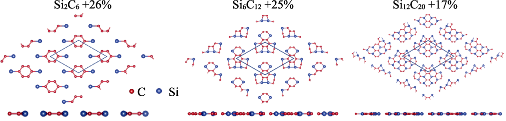
图S4 Si2C6、Si6C12、Si12C20分别在(a) +26%、(b) +25%、(c) +17%双轴应变下的原子结构图(结构发生破坏)
Fig. S4 Optimized atomic structures of Si2C6, Si6C12, and Si12C20 at biaxial strains of (a) +26%, (b) +25%, and (c) +17%, respectively, showing structural failure
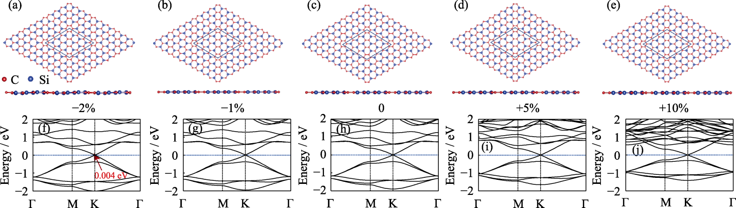
图S5 二维Si12C20在-2%、-1%、0、+5%、+10%双轴应变下的(a~e)原子结构图和(f~j)能带结构图
Fig. S5 (a-e) Optimized atomic structures and (f-j) band structures of 2D Si12C20 under −2%, −1%, 0, +5%, and +10% biaxial strains
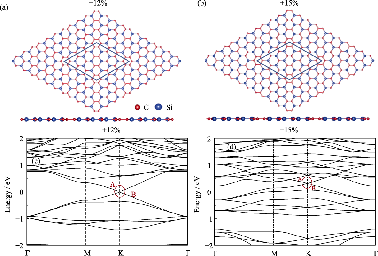
图S6 二维Si12C20在+12%、+15%双轴应变下的(a, b)原子结构图和(c, d)能带结构图
Fig. S6 (a, b) Optimized atomic structures and (c, d) band structures of 2D Si12C20 under +12% and +15% biaxial strains
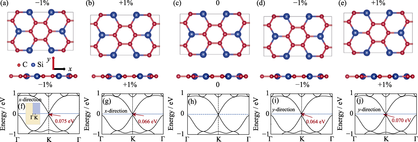
图S7 Si2C6沿x、y方向分别施加-1%、0、+1%单轴应变的(a~e)原子结构图和(f~j)能带结构图
Fig. S7 (a-e) Optimized atomic structures and (f-j) band structure of Si2C6 under -1%, 0, and +1% uniaxial strains along x and y directions (a, b) Optimized atomic structures and (f, g) band structures of Si2C6 under -1% and +1% uniaxial strains along x direction; (c) Optimized atomic structure and (h) band structure of unstrained Si2C6; (d, e) Optimized atomic structures and (i, j) band structures of Si2C6 under -1% and +1% uniaxial strains along y direction
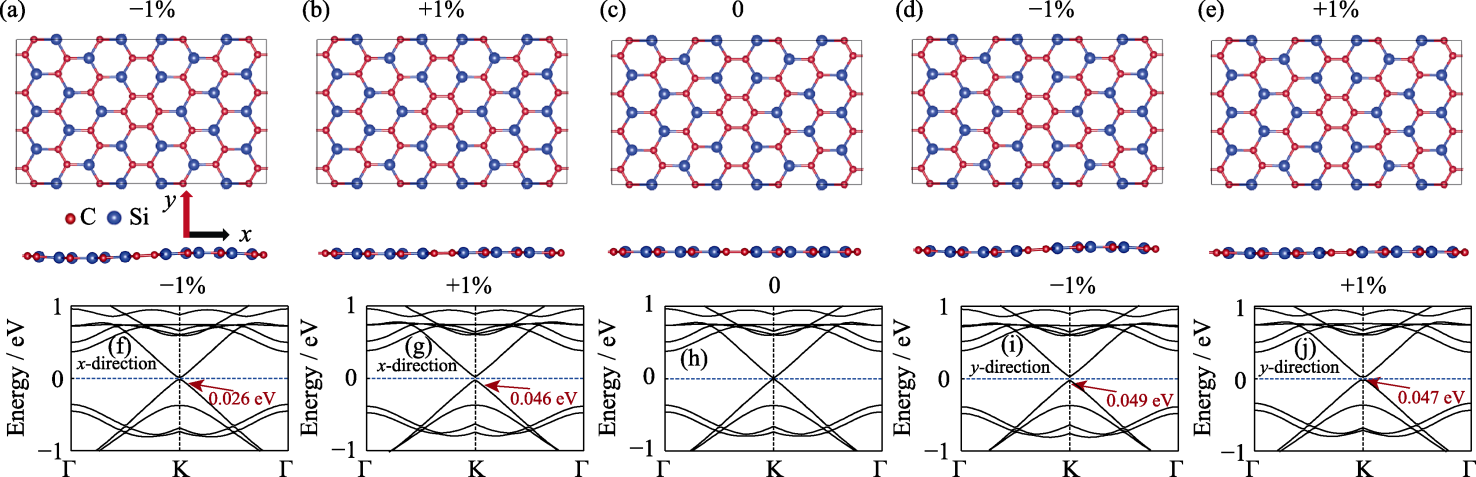
图S8 Si12C20沿x、y方向分别施加-1%、0、+1%单轴应变的(a~e)原子结构图和(f~j)能带结构图
Fig. S8 (a-e) Optimized atomic structures and (f-j) band structure of Si12C20 under -1%, 0, and +1% uniaxial strains along x and y directions (a, b) Optimized atomic structures and (f, g) band structures of Si12C20 under -1% and +1% uniaxial strains along x direction; (c) Optimized atomic structure and (h) band structure of unstrained Si12C20; (d, e) Optimized atomic structures and (i, j) band structures of Si12C20 under -1% and +1% uniaxial strains along y direction

图S9 二维Si6C12在-4%、-3%、0、+5%、+10%双轴应变下基于HSE06杂化泛函的能带结构图
Fig. S9 Band structures of 2D Si6C12 under -4%, -3%, 0, +5%, and +10% biaxial strains based on the HSE06 hybrid functional
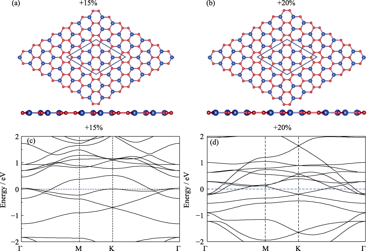
图S10 二维Si6C12在+15%、+20%双轴应变下的(a, b)原子结构图和(c, d)能带结构图
Fig. S10 (a, b) Optimized atomic structures and (c, d) band structures of 2D Si6C12 under +15% and +20% biaxial strains
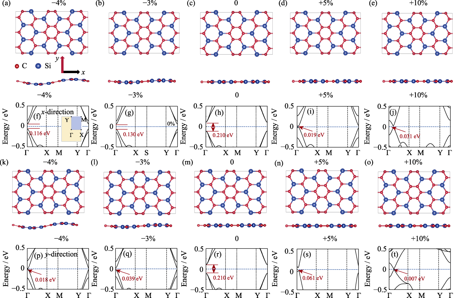
图S11 Si6C12沿x、y方向分别施加-4%、-3%、0、+5%、+10%单轴应变的(a~e)、(k~o)原子结构图和(f~j)、(p~t)能带结构图
Fig. S11 (a-e), (k-o) Optimized atomic structures and (f-j), (p-t) band structures of Si6C12 under -4%, -3%, 0, +5% and +10% uniaxial strains along x and y directions (a-e) Optimized atomic structures and (f-j) band structures of Si6C12 under -4%, -3%, 0, +5% and +10% uniaxial strains along x direction;(k-o) Optimized atomic structures and (p-t) band structures of Si6C12 under -4%, -3%, 0, +5% and +10% uniaxial strains along y direction
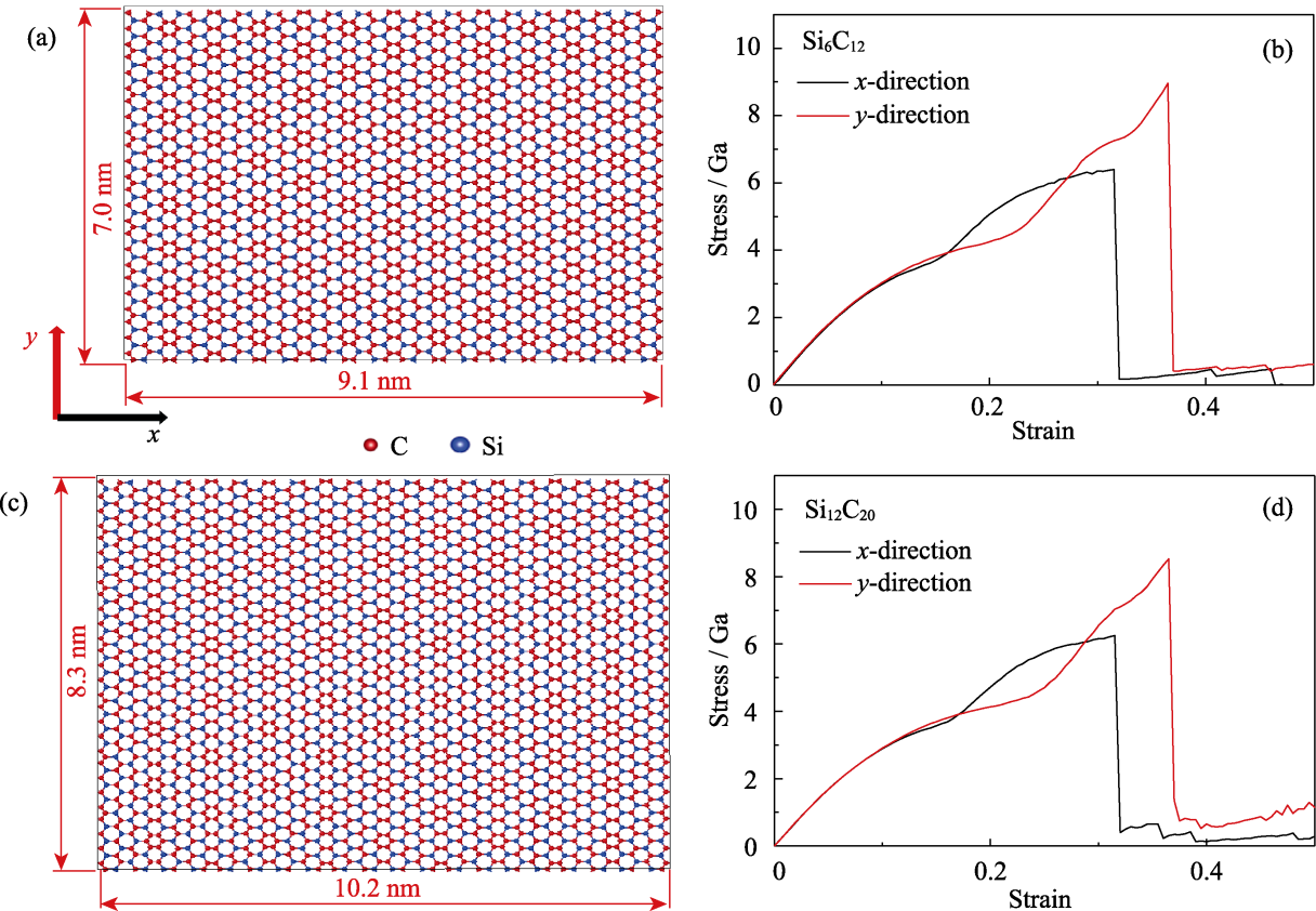
图S12 (a, b) Si6C12、(c, d) Si12C20进行拉伸的(a, c)结构模型图及(b, d)应力-应变曲线
Fig. S12 (a, c) Atomic structural models and (b, d) stress-strain curves of (a, b) Si6C12 and (c, d) Si12C20 during tensile loading
| [1] |
NOVOSELOV K S, GEIM A K, MOROZOV S V, et al. Electric field effect in atomically thin carbon films. Science, 2004, 306(5696): 666.
DOI PMID |
| [2] | MUÑOZ H, ESCAMILLA R O, CERVANTES J M, et al. Theoretical study on the structural, electronic, mechanical, vibrational, thermodynamical, and optical properties of the two- dimensional PbC nanomaterials. Physica Scripta, 2024, 99(1): 18. |
| [3] | CHEN P F, LI N, CHEN X Z, et al. The rising star of 2D black phosphorus beyond graphene: synthesis, properties and electronic applications. 2D Materials, 2018, 5(1): 21. |
| [4] | GUO Z K, TIAN Y, GAN H B, et al. Preparation, structure configuration, physical properties and applications of borophene and two-dimensional alkaline-earth metal boride nanomaterials. Acta Physica Sinica, 2017, 66(21): 13. |
| [5] |
SONG L, LI H, ZHANG Y, et al. Recent progress of two- dimensional metallic transition metal dichalcogenides: syntheses, physical properties, and applications. Journal of Applied Physics, 2022, 131(6): 060902.
DOI URL |
| [6] |
SHI J, HONG M, ZHANG Z, et al. Physical properties and potential applications of two-dimensional metallic transition metal dichalcogenides. Coordination Chemistry Reviews, 2018, 376: 1.
DOI URL |
| [7] |
ZHOU J, LI J, ZHANG J. Intrinsic auxeticity and mechanical anisotropy of Si9C15 siligraphene. Nanoscale, 2023, 15(27): 11714.
DOI URL |
| [8] |
SHU H, GUO J. Enhanced stability and tunable optoelectronic properties of silicon-carbon monolayers by strain and surface functionalization. Journal of Materials Chemistry C, 2024, 12(16): 5916.
DOI URL |
| [9] |
ZHENG J, LI E, CUI Z, et al. Electronic properties of two-dimensional G/GaN (SiC) van der Waals heterostructures. Physica E: Low-dimensional Systems and Nanostructures, 2020, 124: 114277.
DOI URL |
| [10] |
CHO K, YANG J, LU Y. Phosphorene: an emerging 2D material. Journal of Materials Research, 2017, 32(15): 2839.
DOI URL |
| [11] |
WANG H, ZHAO Y, XIE Y, et al. Recent progress in synthesis of two-dimensional hexagonal boron nitride. Journal of Semiconductors, 2017, 38(3): 031003.
DOI URL |
| [12] |
WANG Y, LIU L, MA T, et al. 2D graphitic carbon nitride for energy conversion and storage. Advanced Functional Materials, 2021, 31(34): 2102540.
DOI URL |
| [13] |
POLLEY C, FEDDERWITZ H, BALASUBRAMANIAN T, et al. Bottom-up growth of monolayer honeycomb SiC. Physical Review Letters, 2023, 130(7): 076203.
DOI URL |
| [14] |
GAO Z Y, XU W, GAO Y, et al. Experimental realization of atomic monolayer Si9C15. Advanced Materials, 2022, 34(35): 2204779.
DOI URL |
| [15] |
GAO Y, ZHANG L, ZHANG Y Y, et al. Intrinsic second-order topological insulators produced by triangular Kekulé distortion in honeycomb lattices. Physical Review B, 2024, 110(12): 125103.
DOI URL |
| [16] |
DING Y, WANG Y. Geometric and electronic structures of two- dimensional SiC3 compound. The Journal of Physical Chemistry C, 2014, 118(8): 4509.
DOI URL |
| [17] |
ZHAO M, ZHANG R. Two-dimensional topological insulators with binary honeycomb lattices: SiC3 siligraphene and its analogs. Physical Review B, 2014, 89(19): 195427.
DOI URL |
| [18] |
LIU H, HUANG Z, QIAO H, et al. Characteristics and performance of layered two-dimensional materials under doping engineering. Physical Chemistry Chemical Physics, 2024, 26(25): 17423.
DOI PMID |
| [19] | 冼婧如, 黄煜军, 李昱霖, 等. 单/双轴应变对二维MoSi2N4电子结构与光学性质的影响. 原子与分子物理学报, 2026, 43(4): 159. |
| [20] |
SHARMA N K, SAHOO S, SAHU M C, et al. Electronic bandstructure modulation of MoX2/ZnO (X: S, Se) heterostructure by applying external electric field. Surfaces and Interfaces, 2022, 29: 101817.
DOI URL |
| [21] |
KRESSE G, FURTHMÜLLER J. Efficient iterative schemes for ab initio total-energy calculations using a plane-wave basis set. Physical Review B, 1996, 54(16): 11169.
DOI PMID |
| [22] |
PERDEW J P, BURKE K, ERNZERHOF M. Generalized gradient approximation made simple. Physical Review Letters, 1996, 77(18): 3865.
DOI PMID |
| [23] |
MONKHORST H J, PACK J D. Special points for Brillouin-zone integrations. Physical review B, 1976, 13(12): 5188.
DOI URL |
| [24] | PLIMPTON S. Fast parallel algorithms for short-range molecular dynamics. Journal of Computational Physics, 1995, 117(1): 1. |
| [25] |
ERHART P, ALBE K. Analytical potential for atomistic simulations of silicon, carbon, and silicon carbide. Physical Review B, 2005, 71(3): 035211.
DOI URL |
| [26] |
ISLAM A J, ISLAM M S, FERDOUS N, et al. Anomalous temperature dependent thermal conductivity of two-dimensional silicon carbide. Nanotechnology, 2019, 30(44): 445707.
DOI |
| [27] |
LOPEZ-BEZANILLA A, MARTIN I, LITTLEWOOD P B. Heptagraphene: tunable Dirac cones in a graphitic structure. Scientific Reports, 2016, 6: 33220.
DOI |
| [28] |
ADHIDEWATA J M, KOMALIG R W, UKHTARY M S, et al. Trigonal warping effects on optical properties of anomalous Hall materials. Physical Review B, 2023, 107(15): 155415.
DOI URL |
| [29] |
GOMES Y, RAMOS R O. Tilted Dirac cone effects and chiral symmetry breaking in a planar four-fermion model. Physical Review B, 2021, 104(24): 245111.
DOI URL |
| [30] |
MOSTOFI A A, YATES J R, LEE Y S, et al. Wannier90: a tool for obtaining maximally-localised Wannier functions. Computer Physics Communications, 2008, 178(9): 685.
DOI URL |
| [31] |
WU Q, ZHANG S, SONG H F, et al. WannierTools: an open-source software package for novel topological materials. Computer Physics Communications, 2018, 224: 405.
DOI URL |
| [32] |
WEI X P, ZHANG Y L, SUN X W, et al. Exchange interactions and Curie temperatures in Fe2NiZ compounds. Journal of Alloys and Compounds, 2017, 694: 1254.
DOI URL |
| [33] |
IBRAGIMOVA R, GANCHENKOVA M, KARAZHANOV S, et al. First-principles study of SnS electronic properties using LDA, PBE and HSE 06 functionals. Philosophical Magazine, 2018, 98(8): 710.
DOI URL |
| [34] |
YU M, XIAO X, XIONG Z, et al. Structural, electronic and optical properties of CdGeAs2 with hybrid density functional (HSE06). Materials Today Communications, 2022, 31: 103276.
DOI URL |
| [35] |
ABDULLAH N R, AZEEZ Y H, PIROT B R, et al. High thermal energy storage of the two-dimensional Al2Te3 semiconductor: DFT study of stability, electronic, phonon, thermal, and optical properties based on GGA and HSE06. Physics Letters A, 2024, 528: 130052.
DOI URL |
| [36] |
CHEN M, QUEK S, SHA Z, et al. Effects of grain size, temperature and strain rate on the mechanical properties of polycrystalline graphene-a molecular dynamics study. Carbon, 2015, 85: 135.
DOI URL |
| [37] |
MORTAZAVI B, CUNIBERTI G. Mechanical properties of polycrystalline boron-nitride nanosheets. RSC Advances, 2014, 4(37): 19137.
DOI URL |
| [1] | 吴玉豪, 彭仁赐, 程春玉, 杨丽, 周益春. HfxTa1-xC体系力学性能及熔化曲线的第一性原理研究[J]. 无机材料学报, 2024, 39(7): 761-768. |
| [2] | 张睿, 张侃, 袁梦雅, 谷鑫磊, 郑伟涛. 氮空位调控晶格畸变度强化(NbMoTaW)Nx薄膜的力学性质和耐磨损性[J]. 无机材料学报, 2024, 39(6): 715-725. |
| [3] | 周云凯, 刁亚琪, 王明磊, 张宴会, 王利民. 聚苯胺改性Ti3C2(OH)2抗氧化性的第一性原理计算研究[J]. 无机材料学报, 2024, 39(10): 1151-1158. |
| [4] | 吴晓维, 张涵, 曾彪, 明辰, 孙宜阳. 杂化泛函HSE和PBE0计算CsPbI3缺陷性质的比较研究[J]. 无机材料学报, 2023, 38(9): 1110-1116. |
| [5] | 杨颖康, 邵怡晴, 李柏良, 吕志伟, 王路路, 王亮君, 曹逊, 吴宇宁, 黄荣, 杨长. Cl掺杂对CuI薄膜发光性能增强研究[J]. 无机材料学报, 2023, 38(6): 687-692. |
| [6] | 肖美霞, 李苗苗, 宋二红, 宋海洋, 李钊, 毕佳颖. 表面端基卤化Ti3C2 MXene应用于锂离子电池高容量电极材料的研究[J]. 无机材料学报, 2022, 37(6): 660-668. |
| [7] | 赵宇鹏,贺勇,张敏,史俊杰. 新型二维Zr2CO2/InS异质结可见光催化产氢性能的第一性原理研究[J]. 无机材料学报, 2020, 35(9): 993-998. |
| [8] | 王昌英, 路宇畅, 任翠兰, 王刚, 怀平. 电场、应力和电荷态对Ti2CO2电子性质调控的理论研究[J]. 无机材料学报, 2020, 35(1): 73-78. |
| [9] | 陈雷雷, 邓子旋, 李勉, 李朋, 常可可, 黄峰, 都时禹, 黄庆. 新型MAX相的相图热力学研究[J]. 无机材料学报, 2020, 35(1): 35-40. |
| [10] | 张建峰, 曹惠杨, 王红兵. 新型二维材料MXene的研究进展[J]. 无机材料学报, 2017, 32(6): 561-570. |
| [11] | 乔振杰, 高乐, 冯倩, 胡建宝, 董绍明, 马良来. 硼含量对碳硼化合物结构、力学影响行为研究[J]. 无机材料学报, 2017, 32(11): 1228-1232. |
| [12] | 常希望, 陈 宁, 王丽君, 李福燊, 卞刘振, 周国治. 固体氧化物燃料电池Sr系钙钛矿电极B位元素成分优化规律[J]. 无机材料学报, 2017, 32(10): 1055-1062. |
| [13] | 王晓媛, 嶋田隆広, 北村隆行. 超薄钛酸铅纳米管铁电性和力电耦合特性的第一性原理研究[J]. 无机材料学报, 2014, 29(3): 309-314. |
| [14] | 王志强, 雷雪玲, 吴木生, 刘 刚, 徐 波, 欧阳楚英. 小尺寸锂硅团簇SinLi (n=1~10)的理论研究[J]. 无机材料学报, 2013, 28(11): 1237-1242. |
| [15] | 杨 晓, 刘学建, 黄政仁, 刘桂玲, 姚秀敏. 维氏压痕对常压固相烧结碳化硅陶瓷材料力学性能的影响[J]. 无机材料学报, 2012, 27(9): 965-969. |
| 阅读次数 | ||||||
|
全文 |
|
|||||
|
摘要 |
|
|||||