Journal of Inorganic Materials ›› 2020, Vol. 35 ›› Issue (6): 682-688.DOI: 10.15541/jim20190386
Special Issue: 【虚拟专辑】层状MAX,MXene及其他二维材料
• RESEARCH PAPER • Previous Articles Next Articles
TAN Shilin,YIN Shunda,OUYANG Gang( )
)
Received:2019-07-22
Revised:2019-08-19
Published:2020-06-20
Online:2019-09-04
Supported by:CLC Number:
TAN Shilin,YIN Shunda,OUYANG Gang. Size Effect on the Interface Modulation of Interlayer and Auger Recombination Rates in MoS2/WSe2 van der Waals Heterostructures[J]. Journal of Inorganic Materials, 2020, 35(6): 682-688.
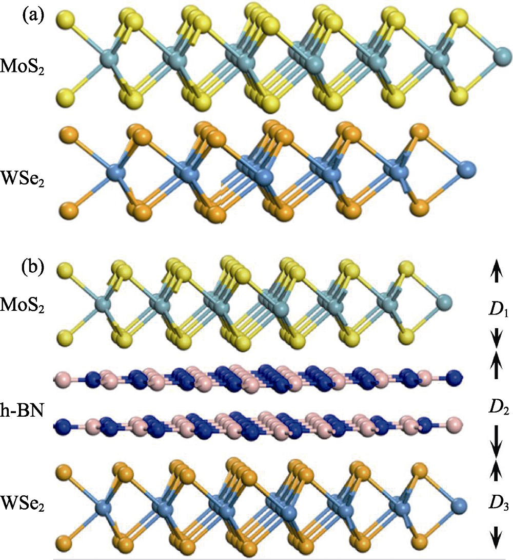
Fig. 1 Schematic diagrams of two kinds of van der Waals heterostructures
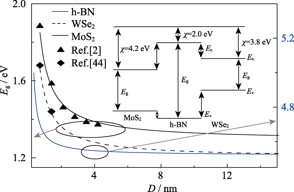
Fig. 2 Thickness-dependent bandgaps of MoS2, WSe2 and h-BN
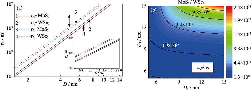
Fig. 3 Thickness-dependent AR lifetime of negative trion (${{\tau }_{{{\text{A}}^{-}}}}$) and biexciton (${{\tau }_{{{\text{A}}^{xx}}}}$) of different system (a) Single component system MoS2 and WSe2; (b) MoS2/WSe2 heterostructures Inset shows the ${{\tau }_{\text{A}}}$under the condition of D<2.0 nm
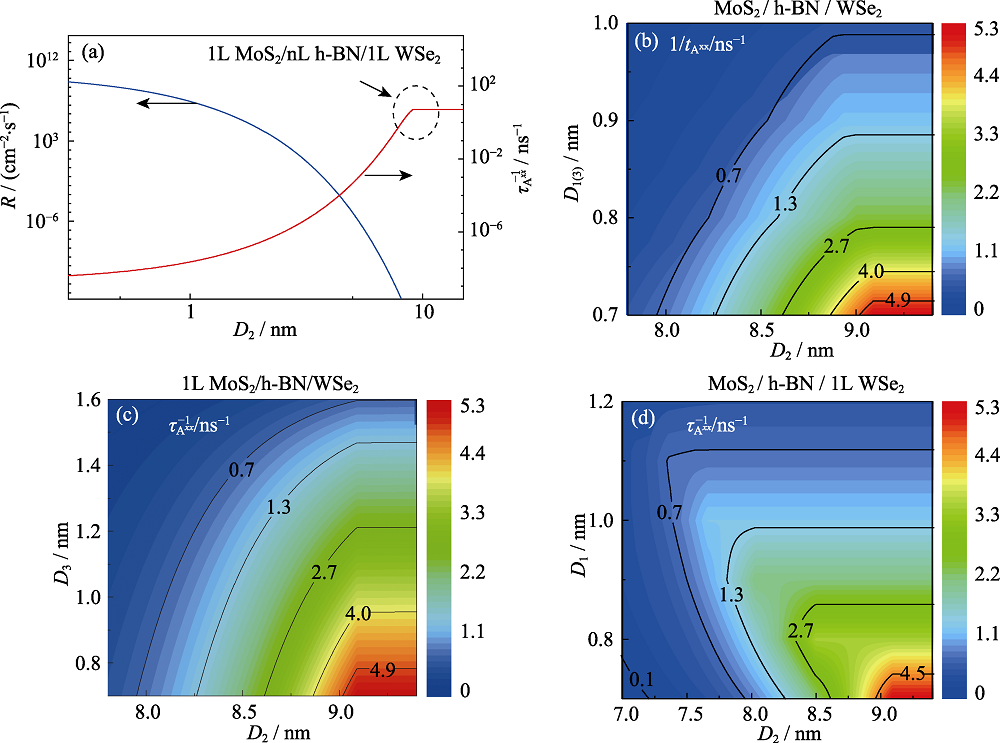
Fig. 4 Thickness-dependent interlayer recombination (R) and biexciton AR rate ($\tau _{{{\text{A}}^{xx}}}^{-1}$) of heterostructures (a) Monolayer MoS2/h-BN/Monolayer WSe2; (b) MoS2/h-BN/WSe2; (c) Monolayer MoS2/h-BN/WSe2; (d) MoS2/h-BN/Monolayer WSe2
| [1] | LI M Y, CHEN C H, SHI Y , et al. Heterostructures based on two-dimensional layered materials and their potential applications. Mater. Today, 2016,19(6):322-335. |
| [2] | MAK K F, LEE C, HONE J , et al. Atomically thin MoS2: a new direct-gap semiconductor. Phys. Rev. Lett., 2010,105(13):136805. |
| [3] | XIAO M, SUN R Z, LI Y F , et al. Transfer printing of VO2 thin films using MoS2/SiO2 van der Waals heterojunctions. J. Inorg. Mater., 2019,34(11):1161-1166. |
| [4] | ZHAO Y, YU W, OUYANG G . Size-tunable band alignment and optoelectronic properties of transition metal dichalcogenide van der Waals heterostructures. J. Phys. D: Appl. Phys., 2017,51(1):015111. |
| [5] | CAO G, SHANG A, ZHANG C , et al. Optoelectronic investigation of monolayer MoS2/WSe2 vertical heterojunction photoconversion devices. Nano Energy, 2016,30:260-266. |
| [6] |
FURCHI M M, ZECHMEISTER A A, HOELLER F , et al. Photovoltaics in van der Waals heterostructures. IEEE J. Sel. Top. Quantum Electron., 2016,23(1):106-116.
DOI URL |
| [7] | CHEN Q, LI Q, YANG Y , et al. Effects of AlGaN interlayer on scattering mechanisms in InAlN/AlGaN/GaN heterostructures. Acta Phys. Sin., 2019,68(1):017301. |
| [8] | FANG H, BATTAGLIA C, CARRARO C , et al. Strong interlayer coupling in van der Waals heterostructures built from single-layer chalcogenides. Proc. Natl. Acad. Sci., 2014,111(17):6198-6202. |
| [9] | LATINI S, WINTHER K T, OLSEN T , et al. Interlayer excitons and band alignment in MoS2/h-BN/WSe2 van der Waals heterostructures. Nano Lett., 2017,17(2):938-945. |
| [10] | KIM J Y, KIM S G, YOUN J W , et al. Energy and charge transfer effects in two-dimensional van der Waals hybrid nanostructures on periodic gold nanopost array. Appl. Phys. Lett., 2018,112(19):193101. |
| [11] | YANG L, YU X, XU M , et al. Interface engineering for efficient and stable chemical-doping-free graphene-on-silicon solar cells by introducing a graphene oxide interlayer. J. Mater. Chem. A, 2014,2(40):16877-16883. |
| [12] | MENG J H, LIU X, ZHANG X W , et al. Interface engineering for highly efficient graphene-on-silicon Schottky junction solar cells by introducing a hexagonal boron nitride interlayer. Nano Energy, 2016,28:44-50. |
| [13] | SUN W F, LI M C, ZHAO L C . First-principles investigation of carrier Auger lifetime and impact ionization rate in narrow-gap superlattices. Acta Phys. Sin., 2010,59(8):5661-5666. |
| [14] | HE Y, OUYANG G . Geometry-dependent Auger recombination process in semiconductor nanostructures. J. Phys. Chem. C, 2017,121(42):23811-23816. |
| [15] | 贺言 . 半导体纳米结构的表/界面以及光电性质的调控研究. 长沙: 湖南师范大学博士学位论文, 2017. |
| [16] | LI Q, LIAN T . Area- and thickness-dependent biexciton Auger recombination in colloidal CdSe nanoplatelets: breaking the “universal volume scaling law”. Nano Lett., 2017,17(5):3152-3158. |
| [17] | LIU S D, CHENG M T, ZHOU H J , et al. The effect of biexciton, wetting layer leakage and Auger capture on Rabi oscillation damping in quantum dots. Acta Phys. Sin., 2006,55(5):2122-2127. |
| [18] | DENNIS A M, MANGUM B D, PIRYATINSKI A , et al. Suppressed blinking and Auger recombination in near-infrared type-II InP/CdS nanocrystal quantum dots. Nano Lett., 2012,12(11):5545-5551. |
| [19] | PARK Y S, BAE W K, PADILHA L A , et al. Effect of the core/shell interface on Auger recombination evaluated by single-quantum-dot spectroscopy. Nano Lett., 2014,14(2):396-402. |
| [20] |
JAIN A, VOZNYY O, HOOGLAND S , et al. Atomistic design of CdSe/CdS core-shell quantum dots with suppressed Auger recombination. Nano Lett., 2016,16(10):6491-6496.
DOI URL |
| [21] | VAXENBURG R, RODINA A, LIFSHITZ E , et al. Biexciton Auger recombination in CdSe/CdS core/shell semiconductor nanocrystals. Nano Lett., 2016,16(4):2503-2511. |
| [22] |
PELTON M, ANDREWS J J, FEDIN I , et al. Nonmonotonic dependence of Auger recombination rate on shell thickness for CdSe/CdS core/shell nanoplatelets. Nano Lett., 2017,17(11):6900-6906.
DOI URL |
| [23] | BEATTIE A R, LANDSBERG P T . Auger effect in semiconductors. Proc. R. Soc. London. Ser. A, 1959,249(1256):16-29. |
| [24] |
LU N, GUO H, WANG L , et al. Van der Waals trilayers and superlattices: modification of electronic structures of MoS2 by intercalation. Nanoscale, 2014,6(9):4566-4571.
DOI URL |
| [25] |
SUN C Q . Size dependence of nanostructures: impact of bond order deficiency. Prog. Solid State Chem., 2007,35(1):1-159.
DOI URL |
| [26] |
OUYANG G, WANG C X, YANG G W . Surface energy of nanostructural materials with negative curvature and related size effects. Chem. Rev., 2009,109(9):4221-4247.
DOI URL |
| [27] | ZHANG A, ZHU Z, HE Y , et al. Structure stabilities and transitions in polyhedral metal nanocrystals: an atomic-bond-relaxation approach. Appl. Phys. Lett., 2012,100(17):171912. |
| [28] | ZHU Z, ZHANG A, OUYANG G , et al. Edge effect on band gap shift in Si nanowires with polygonal cross-sections. Appl. Phys. Lett., 2011,98(26):263112. |
| [29] |
CHEPIC D I, EFROS A L, EKIMOV A I , et al. Auger ionization of semiconductor quantum drops in a glass matrix. J. Lumin., 1990,47(3):113-127.
DOI URL |
| [30] |
OUYANG G, ZHU W G, SUN C Q , et al. Atomistic origin of lattice strain on stiffness of nanoparticles. Phys. Chem. Chem. Phys., 2010,12(7):1543-1549.
DOI URL |
| [31] |
DANOVICH M, ZÓLYOMI V, FAL’KO V I, et al. Auger recombination of dark excitons in WS2 and WSe2 monolayers. 2D Materials, 2016,3(3):035011.
DOI URL |
| [32] |
JIN C, KIM J, WU K , et al. On optical dipole moment and radiative recombination lifetime of excitons in WSe2. Adv. Funct. Mater., 2017,27(19):1601741.
DOI URL |
| [33] |
HUR J H, PARK J, JEON S . A theoretical modeling of photocurrent generation and decay in layered MoS2 thin-film transistor photosensors. J. Phys. D: Appl. Phys., 2017,50(6):065105.
DOI URL |
| [34] |
GUO N, WEI J, JIA Y , et al. Fabrication of large area hexagonal boron nitride thin films for bendable capacitors. Nano Research, 2013,6(8):602-610.
DOI URL |
| [35] | KIRCHARTZ T, MATTHEIS J, RAU U . Detailed balance theory of excitonic and bulk heterojunction solar cells. Phys. Rev. B, 2008,78(23):235320. |
| [36] |
ZEGRYA G G, ANDREEV A D . Mechanism of suppression of Auger recombination processes in type-II heterostructures. Appl. Phys. Lett., 1995,67(18):2681-2683.
DOI URL |
| [37] |
HE Y, QUAN J, OUYANG G . The atomistic origin of interface confinement and enhanced conversion efficiency in Si nanowire solar cells. Phys. Chem. Chem. Phys., 2016,18(10):7001-7006.
DOI URL |
| [38] |
ZHANG C, FU L, ZHAO S , et al. Controllable Co-segregation synthesis of wafe-scale hexagonal boron nitride thin films. Adv. Mater., 2014,26(11):1776-1781.
DOI URL |
| [39] |
KANG J, TONGAY S, ZHOU J , et al. Band offsets and heterostructures of two-dimensional semiconductors. Appl. Phys. Lett., 2013,102(1):012111.
DOI URL |
| [40] | WANG J, MA F, LIANG W , et al. Optical, photonic and optoelectronic properties of graphene, h-BN and their hybrid materials. Nanophotonics, 2017,6(5):943-976. |
| [41] |
VU Q A, LEE J H, NGUYEN V L , et al. Tuning carrier tunneling in van der Waals heterostructures for ultrahigh detectivity. Nano Lett., 2016,17(1):453-459.
DOI URL |
| [42] |
DAS S, PRAKASH A, SALAZAR R , et al. Towards low-power electronics: tunneling phenomena in transition metal dichalcogenides. ACS Nano, 2014,8(2):1681-1689.
DOI URL |
| [43] | CHOI M S, LEE G H, YU Y J , et al. Controlled charge trapping by molybdenum disulphide and graphene in ultrathin heterostructured memory devices. Nat. Commun., 2013,4(1):1624. |
| [44] | YUN W S, HAN S W, HONG S C , et al. Thickness and strain effects on electronic structures of transition metal dichalcogenides: 2H-MX2 semiconductors (M=Mo, W; X=S, Se, Te). Phys. Rev. B, 2012,85(3):033305. |
| [45] | GARCÍA-SANTAMARÍA F, BROVELLI S, VISWANATHA R , et al. Breakdown of volume scaling in Auger recombination in CdSe/CdS heteronanocrystals: the role of the core-shell interface. Nano Lett., 2011,11(2):687-693. |
| [46] |
COHN A W, RINEHART J D, SCHIMPF A M , et al. Size dependence of negative trion Auger recombination in photodoped CdSe nanocrystals. Nano Lett., 2013,14(1):353-358.
DOI URL |
| [47] |
HE Y, HU S, HAN T , et al. Suppression of the Auger recombination process in CdSe/CdS core/shell nanocrystals. ACS Omega, 2019,4(5):9198-9203.
DOI URL |
| [1] | REN Xianpei, LI Chao, LING Fang, HU Qiwei, YU Junling, XIANG Hui, PENG Yuehong. CoMoSSe Alloy with Heterostructure on Carbon Black for Enhanced Electrocatalytic H2 Evolution [J]. Journal of Inorganic Materials, 2025, 40(11): 1293-1299. |
| [2] | MA Rundong, GUO Xiong, SHI Kaixuan, AN Shengli, WANG Ruifen, GUO Ruihua. S-type Heterojunction of MOS2/g-C3N4: Construction and Photocatalysis [J]. Journal of Inorganic Materials, 2023, 38(10): 1176-1182. |
| [3] | LI Tao, CAO Pengfei, HU Litao, XIA Yong, CHEN Yi, LIU Yuejun, SUN Aokui. NH4+ Assisted Interlayer-expansion of MoS2: Preparation and Its Zinc Storage Performance [J]. Journal of Inorganic Materials, 2023, 38(1): 79-86. |
| [4] | LI Wenbo, QIAN Rong, ZHUO Shangjun, JIANG Hong, SHENG Cheng, ZHU Yueqin. MoS2 with Different Morphologies: Preparation and Gas-sensing Property of NH3 [J]. Journal of Inorganic Materials, 2022, 37(10): 1135-1140. |
| [5] | GAO Wa, XIONG Yujie, WU Congping, ZHOU Yong, ZOU Zhigang. Recent Progress on Photocatalytic CO2 Reduction with Ultrathin Nanostructures [J]. Journal of Inorganic Materials, 2022, 37(1): 3-14. |
| [6] | ZHAO Yupeng,HE Yong,ZHANG Min,SHI Junjie. First-principles Study on the Photocatalytic Hydrogen Production of a Novel Two-dimensional Zr2CO2/InS Heterostructure [J]. Journal of Inorganic Materials, 2020, 35(9): 993-998. |
| [7] | DONG Lijia, GUO Xiaojie, LI Xue, CHEN Chaogui, JIN Yang, AHMED Alsaedi, TASAWAR Hayat, ZHAO Qingzhou, SHENG Guodong. Microscopic Insights into pH-dependent Adsorption of Cd(II) on Molybdenum Disulfide Nanosheets [J]. Journal of Inorganic Materials, 2020, 35(3): 293-300. |
| [8] | LIN hai, SU Weitao, ZHU Yu, PENG Pai, FENG Miao, YU Yan. Lattice Control of WO3 Nanoflowers by Heat Treatment and Construction of WO3/CdS/α-S Heterojuntion [J]. Journal of Inorganic Materials, 2020, 35(12): 1349-1356. |
| [9] | ZHAO Shi-Huai, YANG Zi-Bo, ZHAO Xiao-Ming, XU Wen-Wen, WEN Xin, ZHANG Qing-Yin. Green Preparation and Supercapacitive Performance of NiCo2S4@ACF Heterogeneous Electrode Materials [J]. Journal of Inorganic Materials, 2019, 34(2): 130-136. |
| [10] | WEI Ke-Nian, LIU Zhan, ZUO Shi-Xiang, YAN Xiang-Yu, WU Feng-Qin, LI Xia-Zhang, YAO Chao, LIU Xiao-Heng. Preparation of CeO2/Flake-like CdS Composites as High-Performance Photoanodes for Photoelectrochemical Cathodic Protection [J]. Journal of Inorganic Materials, 2019, 34(12): 1334-1340. |
| [11] | HAN Li, ZHANG Xiao-Min, WU De-Yong. MoS2 Quantum Dots Decorated NH2-MIL-125 Heterojunction: Preparation and Visible Light Photocatalytic Performance [J]. Journal of Inorganic Materials, 2019, 34(11): 1205-1209. |
| [12] | HAN Cheng, LEI Yong-Peng, WANG Ying-De. Recent Progress on Nano-heterostructure Photocatalysts for Solar Fuels Generation [J]. Journal of Inorganic Materials, 2015, 30(11): 1121-1130. |
| [13] | LI Ting-Xian, ZHANG Ming, HU Zhou, LI Kuo-She, YU Dun-Bo, YAN Hui. Preparation and Strong Magnetoelectric Effect of Multiferroic BaTiO3/La2/3Sr1/3MnO3 Composite Film [J]. Journal of Inorganic Materials, 2012, 27(3): 291-295. |
| [14] | REN Ming-Fang,WANG Hua. Effect of Annealing Temperature on Structure and Properties of Pt/SrBi2Ta2O9/Bi4Ti3O12/p-Si Heterostructure [J]. Journal of Inorganic Materials, 2008, 23(4): 700-704. |
| [15] | LIANG Hong-Xun,LU Jin-Jun,LIU Wei-Min,XUE Qun-Ji. Study on Self-lubrication Ceramic of Y-TZP/ MoS2 [J]. Journal of Inorganic Materials, 2004, 19(1): 207-213. |
| Viewed | ||||||
|
Full text |
|
|||||
|
Abstract |
|
|||||