Journal of Inorganic Materials ›› 2025, Vol. 40 ›› Issue (2): 196-204.DOI: 10.15541/jim20240343
Special Issue: 【信息功能】功能晶体(202512)
• RESEARCH ARTICLE • Previous Articles Next Articles
HAO Yongxin1,2( ), SUN Jun3(), YANG Jinfeng3, ZHAO Chencheng1,2, LIU Ziqi1,2, LI Qinglian1,2, XU Jingjun1
Received:2024-07-19
Revised:2024-09-02
Published:2025-02-20
Online:2024-11-15
Contact:
SUN Jun, professor. E-mail: sunjun@nankai.edu.cnAbout author:HAO Yongxin (1997-), female, PhD candidate. E-mail: bigcrystal@mail.nankai.edu.cn
Supported by:CLC Number:
HAO Yongxin, SUN Jun, YANG Jinfeng, ZHAO Chencheng, LIU Ziqi, LI Qinglian, XU Jingjun. Twinning Defects in Near-stoichiometric Lithium Niobate Single Crystals[J]. Journal of Inorganic Materials, 2025, 40(2): 196-204.
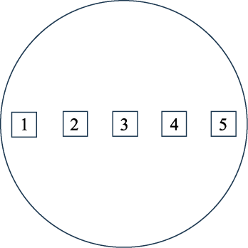
Fig. 1 Schematic diagram of sample locations for wafer Li content testing
| Experiment | Sample | Crystal | Diffusion treatment condition | Results | |||
|---|---|---|---|---|---|---|---|
| Orientation | Size/mm | Temperature/℃ | Time/h | Wafer placement | |||
| 1 | VTE-1-1 | Z-cut | ϕ100×0.86 | 1100 | 120 | Horizontal | Cracked, twins |
| VTE-1-2 | |||||||
| 2 | VTE-2-1 | Z-cut | ϕ100×0.86 | 1100 | 120 | Vertical | Uncracked, twins |
| VTE-2-2 | |||||||
| 3 | VTE-3-Z | Z-cut | ϕ100×1.02 | 1100 | 300 | Vertical | Uncracked, twins |
| VTE-3-X | X-cut | ϕ76.2×0.50 | |||||
| 4 | VTE-4-1 | Z-cut | ϕ100×0.86 | 1100 | 120 | Vertical | Uncracked, twins |
| VTE-4-2 | |||||||
| 5 | VTE-5-1 | Z-cut | ϕ100×0.86 | 1100 | 120 | Vertical | Uncracked, twins |
| VTE-5-2 | Uncracked, without twins | ||||||
| 6 | VTE-6-1 | Z-cut | ϕ100×0.86 | 1100 | 120 | Horizontal | Uncracked, without twins |
| VTE-6-2 | |||||||
| 7 | VTE-7 | Z-cut | ϕ153×1.02 | 1100 | 120 | Horizontal | Uncracked, without twins |
Table 1 Results of crystals diffusion under different conditions
| Experiment | Sample | Crystal | Diffusion treatment condition | Results | |||
|---|---|---|---|---|---|---|---|
| Orientation | Size/mm | Temperature/℃ | Time/h | Wafer placement | |||
| 1 | VTE-1-1 | Z-cut | ϕ100×0.86 | 1100 | 120 | Horizontal | Cracked, twins |
| VTE-1-2 | |||||||
| 2 | VTE-2-1 | Z-cut | ϕ100×0.86 | 1100 | 120 | Vertical | Uncracked, twins |
| VTE-2-2 | |||||||
| 3 | VTE-3-Z | Z-cut | ϕ100×1.02 | 1100 | 300 | Vertical | Uncracked, twins |
| VTE-3-X | X-cut | ϕ76.2×0.50 | |||||
| 4 | VTE-4-1 | Z-cut | ϕ100×0.86 | 1100 | 120 | Vertical | Uncracked, twins |
| VTE-4-2 | |||||||
| 5 | VTE-5-1 | Z-cut | ϕ100×0.86 | 1100 | 120 | Vertical | Uncracked, twins |
| VTE-5-2 | Uncracked, without twins | ||||||
| 6 | VTE-6-1 | Z-cut | ϕ100×0.86 | 1100 | 120 | Horizontal | Uncracked, without twins |
| VTE-6-2 | |||||||
| 7 | VTE-7 | Z-cut | ϕ153×1.02 | 1100 | 120 | Horizontal | Uncracked, without twins |

Fig. 2 4-inch (100 nm) Z-cut LN wafers obtained from VTE experiments 1-6 (a) VTE-1-1; (b) VTE-1-2; (c) VTE-2-1; (d) VTE-2-2; (e) VTE-3-Z; (f) VTE-3-X; (g) VTE-4-1; (h) VTE-4-2; (i) VTE-5-1; (j) VTE-5-2; (k) VTE-6-1; (l) VTE-6-2
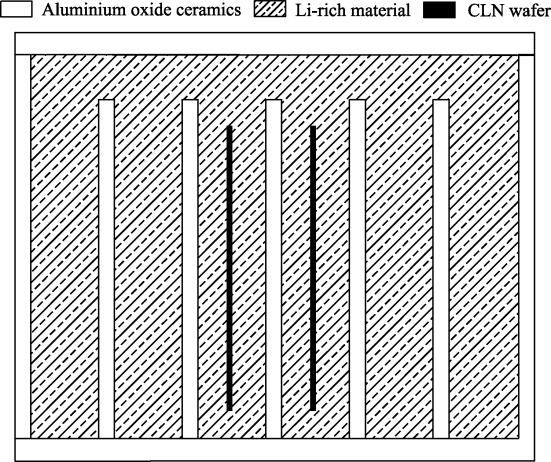
Fig. 3 Schematic diagram of experimental device for the 4th VTE experiment
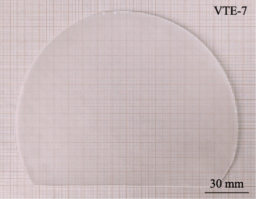
Fig. 4 6-inch (153 nm) Z-cut nSLN wafer obtained from the 7th VTE experiment (VTE-7)
| Sample | TC/℃ | Average of TC/℃ | CLi/% (in mole) | |
|---|---|---|---|---|
| VTE-5-2 | 1 | 1200 | 1200.2 | 49.94 |
| 2 | 1201 | |||
| 3 | 1200 | |||
| 4 | 1201 | |||
| 5 | 1199 | |||
| VTE-6-1 | 1 | 1202 | 1201.6 | 49.98 |
| 2 | 1201 | |||
| 3 | 1202 | |||
| 4 | 1201 | |||
| 5 | 1202 | |||
| VTE-7 | 1 | 1202 | 1201.0 | 49.96 |
| 2 | 1201 | |||
| 3 | 1200 | |||
| 4 | 1201 | |||
| 5 | 1201 | |||
Table 2 Curie temperatures (TC) and Li contents (CLi) of different wafers
| Sample | TC/℃ | Average of TC/℃ | CLi/% (in mole) | |
|---|---|---|---|---|
| VTE-5-2 | 1 | 1200 | 1200.2 | 49.94 |
| 2 | 1201 | |||
| 3 | 1200 | |||
| 4 | 1201 | |||
| 5 | 1199 | |||
| VTE-6-1 | 1 | 1202 | 1201.6 | 49.98 |
| 2 | 1201 | |||
| 3 | 1202 | |||
| 4 | 1201 | |||
| 5 | 1202 | |||
| VTE-7 | 1 | 1202 | 1201.0 | 49.96 |
| 2 | 1201 | |||
| 3 | 1200 | |||
| 4 | 1201 | |||
| 5 | 1201 | |||
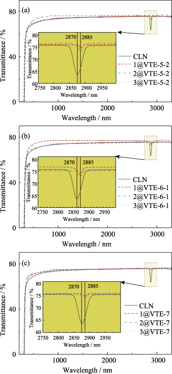
Fig. 5 Transmission spectra of CLN wafer and nSLN wafers (a) VTE-5-2; (b) VTE-6-1; (c) VTE-7
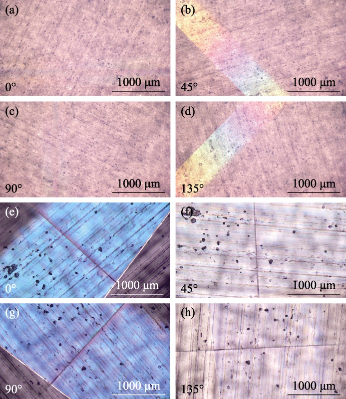
Fig. 6 Birefringence changes in the twinning regions of wafers VTE-3-Z and VTE-3-X rotated at different angles within 180° (a) 0°-VTE-3-Z; (b) 45°-VTE-3-Z; (c) 90°-VTE-3-Z; (d) 135°-VTE- 3-Z; (e) 0°-VTE-3-X; (f) 45°-VTE-3-X; (g) 90°-VTE-3-X; (h) 135°-VTE- 3-X
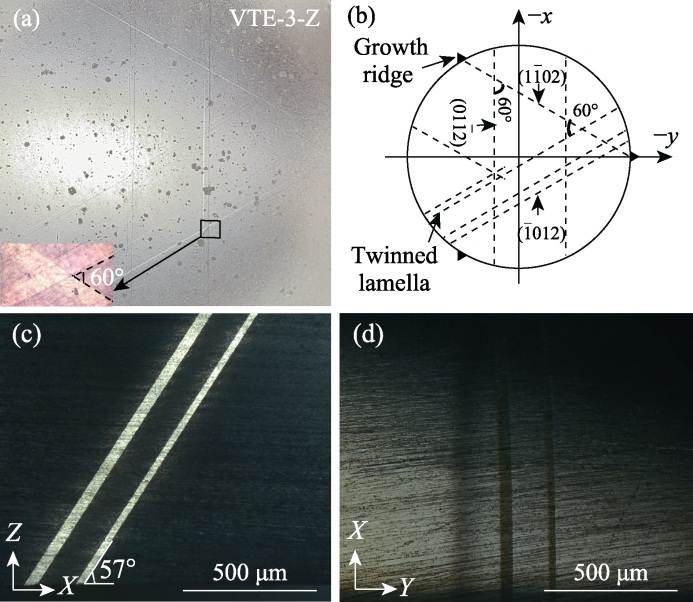
Fig. 7 Direction of the twinned lamella on the Z-cut wafer after VTE process (a) Wafer VTE-3-Z; (b) Schematic diagram of VTE-3-Z; (c) Angle between the twinned lamella and the Z-plane is 57°; (d) Angle between the twinned lamella and the X-plane is 90°
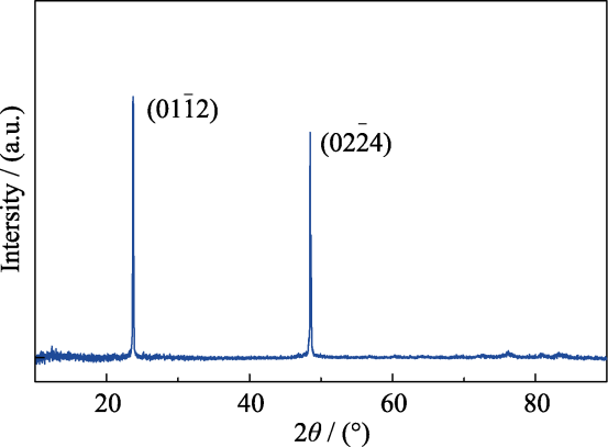
Fig. 8 X-ray diffraction pattern of the twinning plane within the wafer VTE-1-1
| Family of LN crystal planes | Angle | Family of LN crystal planes | Angle |
|---|---|---|---|
| 90° | 90° | ||
| 72°10′ | 74°26′ | ||
| 37°52′ | 57°15′ | ||
| 60°53′ | 21°14′ | ||
| 41°55′ | 80°52′ |
Table 3 Angles between families of crystal planes and (0001) plane of LN crystal[22]
| Family of LN crystal planes | Angle | Family of LN crystal planes | Angle |
|---|---|---|---|
| 90° | 90° | ||
| 72°10′ | 74°26′ | ||
| 37°52′ | 57°15′ | ||
| 60°53′ | 21°14′ | ||
| 41°55′ | 80°52′ |
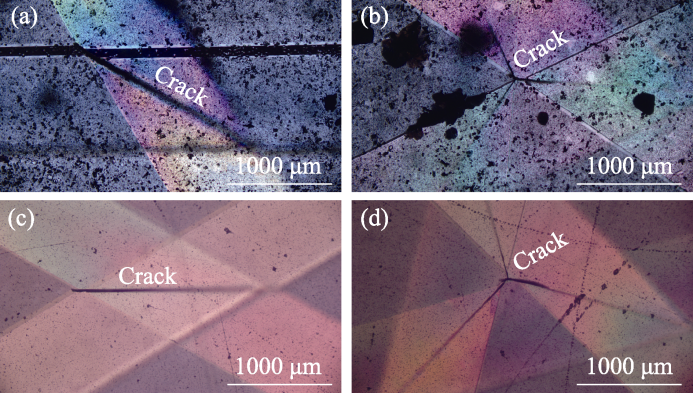
Fig. 9 Cracks at crossing of twins on Z-cut wafers before and after polishing (a) Two twinned lamella (before polishing); (b) Three twinned lamella (before polishing); (c) Two twinned lamella (after polishing); (d) Three twinned lamella (after polishing)
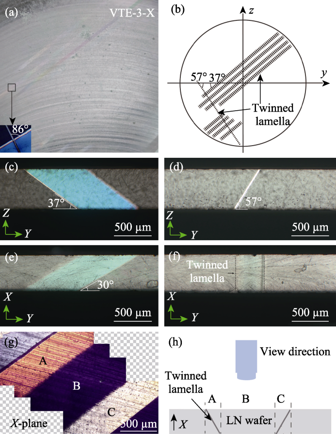
Fig. 10 Direction of the twinned lamella on the X-cut wafer after VTE process (a) Wafer VTE-3-X; (b) Schematic diagram of VTE-3-X; (c) Angle between the wider twinned lamella and the Z-plane is 37°; (d) Angle between the narrower twinned lamella and the Z-plane is 57°; (e) Angle between the wider twinned lamella and the Y-axis is 30°; (f) Angle between the projection of the narrower twinned lamella and the Y-axis is 90°; (g) Projections of ( 1 1 ¯ 02 ) and ( 1 ¯ 012 ) on the X-plane; (h) Schematic diagram of observation directions ( 1 1 ¯ 02 ) and ( 1 ¯ 012 )
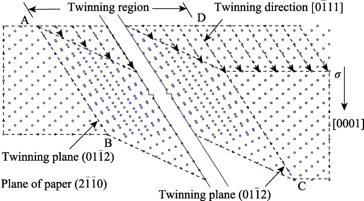
Fig. 11 Slip of niobium atoms (or lithium atoms) during twinning deformation of LN crystal
| [1] | ZHENG Y L, CHEN X F. Integrated nonlinear photonics on thin-film lithium niobate: a route to an all-optical information era. Physics, 2024, 53(1): 22. |
| [2] | KONG Y F, BO F, WANG W W, et al. Recent progress in lithium niobate: optical damage, defect simulation, and on-chip devices. Advanced Materials, 2020, 32(3): 1806452. |
| [3] | QI Y F, LI Y. Integrated lithium niobate photonics. Nanophotonics, 2020, 9(6): 1287. |
| [4] | XIE Z D, ZHU S N. LiNbO3 crystals: from bulk to film. Advanced Photonics, 2022, 4(3): 30502. |
| [5] | REISMAN A, HOLTZBERG F. Heterogeneous equilibria in the systems Li2O-, Ag2O-Nb2O5 and oxide-model. Journal of the American Chemical Society, 1958, 80(24): 6503. |
| [6] | TAN S F, LI J T, ZHANG L, et al. Progress in the preparation of near stoichiometric ratio lithium niobate crystals. Science & Technology Information, 2009(11): 6. |
| [7] | WANG H C, ZHANG Y, XIANG D, et al. Growth and mechanical properties of near-stoichiometric LiNbO3 crystal. Optik, 2018, 164: 385. |
| [8] | WANG F L, SUN D H, LIU Q L, et al. Growth of large size near-stoichiometric lithium niobate single crystals with low coercive field for manufacturing high quality periodically poled lithium niobate. Optical Materials, 2022, 125: 112058. |
| [9] | YAO S, WANG J, LIU H, et al. Growth, optical and thermal properties of near-stoichiometric LiNbO3 single crystal. Journal of Alloys and Compounds, 2008, 455(1/2): 501. |
| [10] | YATSENKO A, YEVDOKIMOV S, PALATNIKOV M, et al. NMR spectra particularities in LiNbO3 crystals with a near- stoichiometric composition. Ceramics, 2023, 6(1): 432. |
| [11] | PALATNIKOV M, SIDOROV N, KADETOVA A, et al. Growing, structure and optical properties of LiNbO3: B crystals, a material for laser radiation transformation. Materials, 2023, 16(2): 732. |
| [12] | GRESHNYAKOV E D, LISJIKH B I, AKHMATKHANOV A R, et al. Charged domain walls in lithium niobate and lithium tantalate crystals with composition gradient. Ferroelectrics, 2023, 604(1): 32. |
| [13] | LENGYEL K, PÉTER Á, KOVÁCS L, et al. Growth, defect structure, and THz application of stoichiometric lithium niobate. Applied Physics Reviews, 2015, 2(4): 40601. |
| [14] | SUN J, LI Q L, YANG J F, et al. Preparation of large size near stoichiometric lithium niobate crystals. Journal of synthetic crystals, 2015, 44(12): 3423. |
| [15] | BHATT R, BHAUMIK I, GANESAMOORTHY S, et al. Study of structural defects and crystalline perfection of near stoichiometric LiNbO3 crystals grown from flux and prepared by VTE technique. Journal of Molecular Structure, 2014, 1075: 377. |
| [16] | FURUKAWA Y, SATO M, KITAMURA K, et al. Growth and characterization of off-congruent LiNbO3 single crystals grown by the double crucible method. Journal of Crystal Growth, 1993, 128(1-4): 909. |
| [17] | 高磊. 近化学计量比铌酸锂晶体生长与性质研究. 济南: 山东大学博士学位论文, 2006. |
| [18] | SUN J, KONG Y, ZHANG L, et al. Growth of large-diameter nearly stoichiometric lithium niobate crystals by continuous melt supplying system. Journal of Crystal Growth, 2006, 292(2): 351. |
| [19] | 孙军. 高性能铌酸锂晶体与光电器件产品化的关键技术研究. 天津: 南开大学博士学位论文, 2008. |
| [20] | YANG J F, HUANG C X, SUN J, et al. Study on precise determination of lithium content in the LiNbO3 crystals. Journal of Synthetic Crystals, 2014, 43(4): 738. |
| [21] | YANG J F, LAI M M, SHANG J F, et al. Defect structure of near-stoichiometric Mg-doped LiNbO3 crystals prepared by different method. Journal of Crystal Growth, 2022, 580: 126478. |
| [22] | 李德宇, 陈家平, 侯朝阳. 关于铌酸锂(LN)和钽酸锂(LT)晶体的若干结晶学问题. 硅酸盐学报, 1978, 6(1/2): 1. |
| [23] | VERE A W. Mechanical twinning and crack nucleation in lithium niobate. Journal of Materials Science, 1968, 3: 617. |
| [24] | KALANTARIAN A H, MAYILYAN G L, GLADUN A D, et al. On crossings of twins in lithium niobate crystals. Philosophical Magazine A, 1997, 76(2): 319. |
| [25] | PARK B M, KITAMURA K, TERABE K, et al. Mechanical twinning in stoichiometric lithium niobate single crystal. Journal of Crystal Growth, 1997, 180(1): 101. |
| [26] | FRIES E, PÉTER A. Plastic deformation of LiNbO3 single crystals. Revue de Physique Appliquée, 1987, 22(11): 1353. |
| [27] | OKADA Y, IIZUKA T. An X-ray topographic study of dislocations in a LiNbO3 crystal. Journal of Applied Crystallography, 1976, 9(5): 375. |
| [1] | ZOU Jun,ZHOU Sheng-Ming,ZHANG Lian-Han,XU Jun. Preparation of Large-size and High-quality γ-LiAlO2 Crystal [J]. Journal of Inorganic Materials, 2006, 21(1): 17-21. |
| [2] | LI Shu-Zhi,XU Jun,YANG Wei-Qiao,ZHOU Jun,ZHOU Sheng-Ming. γ-LiAlO2 Layer on (0001) Sapphire Fabricated by Vapor Transport Equilibration [J]. Journal of Inorganic Materials, 2005, 20(1): 169-174. |
| Viewed | ||||||
|
Full text |
|
|||||
|
Abstract |
|
|||||