

半导体氮化镓(GaN)材料具有直接带隙、禁带宽度大、热导系数高、击穿电场强度高以及电子迁移率高等优异特性[1], 被广泛应用于电子器件和光电子器件中, 如高电子迁移率晶体管(High Electron Mobility Transistor, HEMT)[2]、发光二极管(Light Emitting Diode, LED)[3⇓-5]、激光二极管(Laser Diode, LD)[6]和紫外探测器(Ultraviolet Photodetector, UV PD)[7]等。目前通过多种外延方式均可获得GaN单晶材料, 其中金属有机化学气相淀积(Metal Organic Chemical Vapor Deposition, MOCVD)具有外延质量好、反应速率快、重复性高和产量大等优点[8], 是制备GaN最常用的方法。
使用MOCVD制备GaN时, 常用异质外延的方式, 其中蓝宝石衬底以成本低、尺寸小和工艺成熟等特点, 成为外延GaN的主要衬底之一。而GaN与蓝宝石衬底之间存在较大的晶格失配和热失配, 由此产生的大量位错会使器件性能退化。因此, 制备高质量GaN时, 常需要氮化铝(AlN)材料作为成核层。AlN成核层为外延GaN提供了与衬底取向相同的成核中心, 同时释放了GaN与衬底间的晶格失配应力和热膨胀失配应力[9], 有利于后续GaN材料的二维(2D)生长。AlN成核层的常用制备方法有MOCVD的两步生长法和磁控溅射法[10], 也可使用分子束外延法[11]。等离子体增强原子层沉积(Plasma-enhanced Atomic Layer Deposition, PEALD)技术也可用于制备AlN薄膜材料[12⇓-14], 其特点是能在真空和低温环境下实现单原子层沉积[15], 从而获得低杂质浓度、高质量的AlN薄膜。这种方法制备的AlN材料已经用于多种半导体器件中[16⇓-18], 但是目前少有将PEALD制备的AlN作为成核层外延生长单晶GaN的报道。本研究提出在蓝宝石上使用PEALD制备AlN来外延生长单晶GaN, 探究不同厚度的AlN作为成核层对GaN外延层质量的影响, 寻找AlN作为成核层的最佳厚度。
1 实验方法
1.1 PEALD制备AlN
本实验使用ALD-150PE设备在c面蓝宝石衬底上沉积AlN, 设置反应温度为200 ℃, 开启射频电源, 沉积工艺如图1所示, 具体步骤如下: 通入0.03 s的TMA→通入30 s的Ar进行吹扫→通入10 s的流量为20 sccm的N2-plasma→通入20 s的Ar进行吹扫。
图1
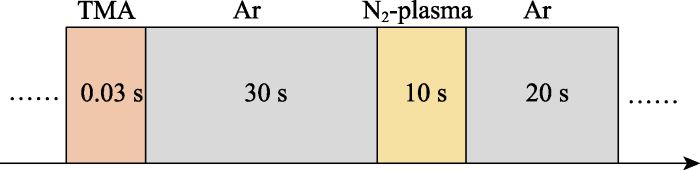
图1
PEALD工艺制备AlN的示意图
Fig. 1
Schematic diagram of plasma-enhanced atomic layer deposition (PEALD) process of AlN
设置沉积循环周期数, 便可获得不同厚度的AlN。在两寸蓝宝石衬底上循环沉积125、208、292和333周AlN, 分别记为样品1、样品2、样品3和样品4。其中样品1、样品2和样品3用于外延GaN, 样品4用来测试AlN的沉积速率。
1.2 MOCVD外延GaN
MOCVD是一种化学气相沉积技术, 由1968年Manasevit[24]提出的制备化合物半导体单晶薄膜材料的方法发展而来。对于氮化物的制备, MOCVD采用H2或N2作为载气, 把源气瓶中的金属有机化合物(如三甲基镓(TMGa)、三甲基铟(TMIn)和TMA等)传输到反应室, 并与同时到达的NH3在衬底表面发生化学反应, 生成所需氮化物, 剩余气体则通入尾气处理系统。
本工作使用VEECO K465I型号的MOCVD设备, 在沉积AlN后的样品1、样品2和样品3上进行GaN的外延生长, 具体外延工艺条件: 反应温度为1080 ℃, 压力为26660 Pa; 使用TMGa作为反应Ga源, 流量为630 sccm; 使用NH3作为反应N源, 流量为822 sccm; 使用H2和N2作为载气, 流量分别为1644和740 sccm。
利用MOCVD的原位检测系统,可以在反应过程中检测薄膜生长速率等参数, 最终制得6 μm 厚的GaN,样品1、样品2和样品3外延得到的GaN分别记为样品a、样品b和样品c。
2 沉积AlN层表征与讨论
2.1 PEALD制备AlN速率验证
图2
2.2 AlN形貌表征
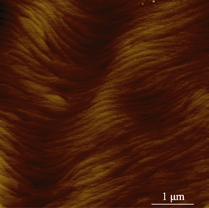
使用NX20原子力显微镜(Atomic Force Microscope, AFM) 观察沉积AlN后样品的表面形貌, 其1 μm×1 μm尺寸的3D形貌如图3所示。沉积的AlN会在蓝宝石衬底上形成一种岛状的特殊形貌, 这与PEALD工艺制备AlN的报道相同[20]。通过对比三组样品的AFM图, 可以观察到随着沉积厚度增大, 样品表面的小岛形貌变化明显。沉积12.5 nm厚AlN时, 小岛高度和体积较小, 大小和分布较不均匀, 表明开始形成小岛形状; 沉积20.8 nm厚AlN时, 小岛高度和体积适中, 大小和分布较为均匀, 且小岛数量最多; 沉积29.2 nm厚AlN时, 小岛高度和体积较大, 大小和分布较不均匀, 这与小岛之间的合并有关。
图3
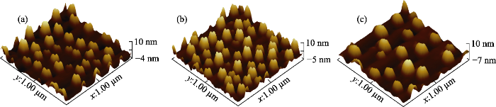
图3
AlN的表面形貌
Fig. 3
Surface topographies of AlN
AFM 3D images of (a) sample 1, (b) sample 2 and (c) sample 3
2.3 AlN晶体质量表征
图4
3 外延GaN表征与讨论
3.1 GaN形貌表征
对完成了外延生长GaN的三组样品进行形貌测试, 使用Sigma-300扫描电子显微镜(Scanning Electron Microscopy, SEM)观察三组样品的表面形貌。在2k倍镜下观察三组样品表面形貌, 如图5所示。样品b表面平滑, 而样品a和样品c表面没有合并, 呈现台阶和颗粒状。样品a具有更大的晶粒, 样品c表面布满较小的颗粒, 说明样品a和样品c都有多晶化的趋势。
图5
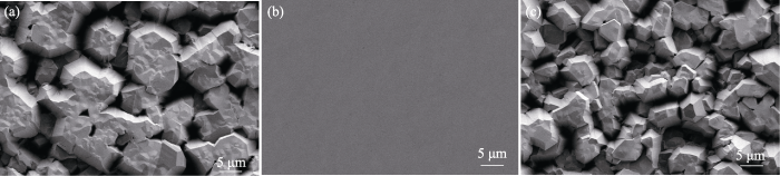
图5
GaN的SEM照片
Fig. 5
SEM images of GaN
(a) Sample a; (b) Sample b; (c) Sample c
图6
结合图3和图6的AFM图像以及图5的SEM图像结果分析, 样品b具有最好的表面形貌, 说明PEALD制备的20.8 nm厚度的AlN成核层最有利于GaN生长, 获得的GaN表面最平坦。GaN表面形貌的差异与沉积AlN提供的成核机理有关[28], 样品a和样品c表面未合并, 呈现颗粒状。根据AlN薄膜的表面形貌分析可知, 对于样品c, 由于沉积的AlN较厚(29.2 nm), 在蓝宝石衬底上提供了较大的成核岛且成核岛间距较大, 使GaN更倾向于在这些大岛上生长, GaN的三维(3D)生长模式得到增强。对于样品a, 由于沉积的AlN较薄(12.5 nm), 在蓝宝石衬底上刚开始形成成核岛, 成核岛体积较小且数量不多, 成核岛的大小和分布不太均匀, 使GaN生长介于2D生长模式和3D生长模式之间, 因此其表面没有连接起来形成统一的平面。对于样品b, 由于沉积AlN的厚度合适(20.8 nm), 在蓝宝石衬底上形成大小适中、数量最多, 且大小和分布十分均匀的成核岛, 给外延的GaN提供了非常合适的成核点, 因而获得的GaN表面最平坦。
3.2 GaN光学表征
为了研究外延GaN的应力状态, 使用Alpha300RS设备对三组样品进行了拉曼(Raman)测试, 结果如图7所示。无应变GaN的E2(high)峰的频率为567.6 cm-1, 当GaN受到压应力时该散射峰的波数变大[29]。图7可知样品a、样品b和样品c的E2(high)峰频率分别为568.7、569.9和570.4 cm-1; 半峰全宽(Full Width at Half Maximum, FWHM)分别为4.78、3.64和5.57 cm-1。三组样品的E2(high)峰频率都大于567.6 cm-1, 说明所有样品均处于压应力状态, 这是蓝宝石与GaN的热膨胀系数不同所导致的。蓝宝石的热膨胀系数较大, 会对外延的GaN产生压应力[30]。对比样品a、样品b和样品c, 发现沉积AlN越薄, 外延GaN所受到压应力越小。因此调节沉积AlN层的厚度可以改变外延GaN的应力大小。样品b的E2(high)峰的FWHM最小, 表明样品b的结晶质量最好。沿着GaN的[0001]晶向入射Raman光时, 测试光谱中除了有明显的E2(high)峰, 还会在735 cm-1附近出现A1(LO)散射峰。对比三组样品, 从样品b的Raman图谱中还能观察到明显的A1(LO)散射峰, 频率为736.2 cm-1, FWHM为7.74 cm-1, 这也证明样品b具有最好的结晶质量[30-31]。
图7
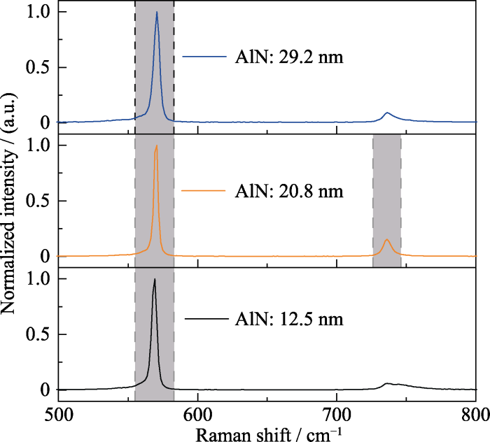
图7
在不同厚度AlN成核层外延GaN的Raman光谱
Fig. 7
Raman spectra of epitaxial GaN on AlN nucleation layers with different thicknesses
为了研究GaN样品的光学特性, 使用EtaMax光致发光(Photoluminescence, PL)设备对三组GaN进行测试。在激光波长为266 nm, 功率为8 mW的条件下, 三组样品测试结果如图8所示。样品a、样品b和样品c的FWHM分别为14.39、10.94和14.21 nm。样品2的FWHM最小, 表明其具有最好的光学特性, 这与Raman测试结果相符合。
图8
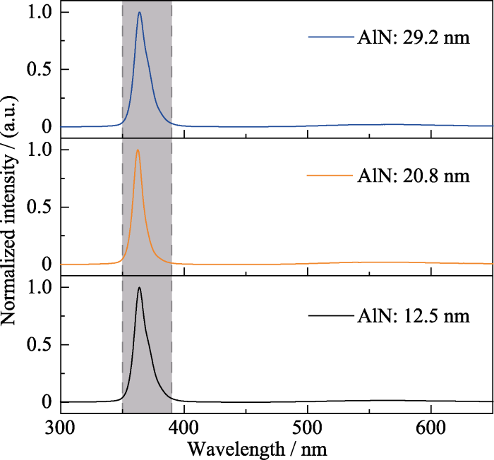
图8
不同厚度AlN成核层的GaN的PL光谱图
Fig. 8
PL spectra of GaN with different thicknesses of AlN nucleation layers
3.3 GaN晶体质量表征
为了研究不同AlN厚度对外延GaN结晶质量的影响, 使用χ'Pert3 MRD高分辨X射线衍射(High Resolution X-ray Diffraction, HRXRD)仪对样品进行测试, 获得GaN材料的摇摆曲线。在纤锌矿结构中, 螺位错密度(Screw Dislocation Density, Dscrew)与(002)晶面上摇摆曲线FWHM的平方成正比, 刃位错密度(Edge Dislocation Density, Dedge)与(102)晶面上摇摆曲线FWHM的平方成正比, 总位错密度(Total Dislocation Density, Dtotal)为二者之和, 具体表达式如式(1)所示[32]。
式(1)中b(002)和b(102)分别是(002)晶面和(102)晶面的伯格斯矢量(Burgers Vector), 取值分别为5.185×10⁻⁸和3.189×10⁻⁸ cm。对样品b进行测试, 结果如图9所示。样品b的(002)晶面摇摆曲线FWHM为681 arcsec, 计算得Dscrew为9.30×108 cm-2;(102)晶面摇摆曲线FWHM为1265 arcsec, 计算得Dedge为8.48×109 cm-2, 所以Dtotal为9.41×109 cm-2。
图9
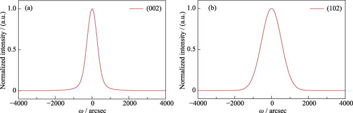
图9
样品b不同晶面的摇摆曲线
Fig. 9
Rocking curves of sample b on different crystal planes
(a) (002); (b) (102)
对样品a和样品c进行测试, 结果如图10所示。由于样品a和样品c表面呈现颗粒状, 所以二者(002)晶面摇摆曲线的FWHM特别大, 分别为12197和21034 arcsec, 根据式(1)计算得到Dscrew分别为2.98×10¹¹和8.87×1011 cm-2, 比样品b的Dscrew高了3个数量级, 说明样品b的晶体质量远优于样品a和样品c。此外, 样品a和样品c的(102)晶面摇摆曲线无法测出, 也说明样品a和样品c晶体质量不佳。总之, 三组样品的HRXRD的测试结果表明样品b的GaN晶体质量最好。
图10
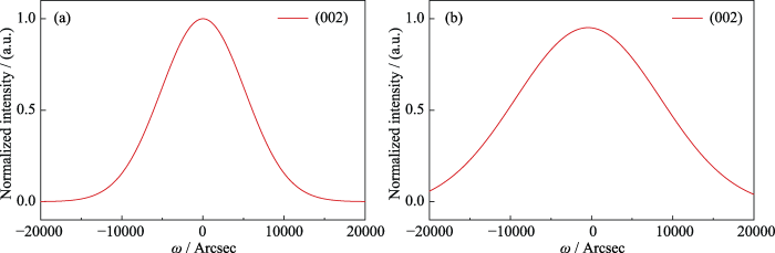
图10
样品a(a)和样品c(b)(002)晶面的摇摆曲线
Fig. 10
Rocking curves of (002) crystal plane for sample a (a) and sample c (b)
4 结论
本研究在蓝宝石衬底上使用PEALD设备沉积的AlN作为成核层外延了单晶GaN,实验中制备了三组不同AlN厚度的样品作为对照,探究了厚度对外延GaN的影响。在对AlN的测试中发现,沉积AlN厚度的变化会导致AlN表面成核岛的大小和分布情况发生变化,进一步导致后续外延GaN的质量发生变化。测试结果表明,对于较薄(12.5 nm)和较厚(29.2 nm)的AlN成核层,AlN成核岛的尺寸差异较大并且分布不均匀,不利于外延单晶GaN,最终导致其上外延GaN的表面尚未合并。当AlN成核层厚度为20.8 nm时,AlN成核岛的尺寸合适并分布均匀,有利于外延单晶GaN,其上外延的GaN表明平坦,Rms为0.272 nm,并且具有更好的光学特性,其晶体质量更是得到极大提升,Dscrew相比于另外两组样品降低了3个数量级。总之,本研究实现了在PEALD设备沉积AlN上单晶GaN的外延生长,该技术为获取高质量氮化物了提供了一种新的方法。
参考文献
Transient electron transport in wurtzite GaN, InN, and AlN
High-power polarization- engineered GaN/AlGaN/GaN HEMTs without surface passivation
Key inventions in the history of nitride-based blue LED and LD
Improved crystal quality and enhanced optical performance of GaN enabled by ion implantation induced high-quality nucleation

Hetero-epitaxial growth of GaN often leads to high density of threading dislocations, which poses a significant challenge to the promotion of the performance of GaN-based devices. In this study, we address this issue by utilizing an Al-ion implantation pretreatment on sapphire substrates, which induces high-quality regularly arranged nucleation and promotes the crystal quality of GaN. Specifically, we demonstrate that an Al-ion dose of 10cm leads to a reduction of full width at half maximum values of (002)/(102) plane X-ray rocking curves from 204.7/340.9 arcsec to 187.0/259.5 arcsec. Furthermore, a systematic investigation of GaN film grown on the sapphire substrate with various Al-ion doses is also performed, and the nucleation layer growth evolution on different sapphire substrates is analyzed. As confirmed by the atomic force microscope results of the nucleation layer, the ion implantation induced high-quality nucleation is demonstrated, which results in the improved crystal quality of the as-grown GaN films. Transmission electron microscope measurement also proves the dislocation suppression through this method. In addition, the GaN-based light-emitting diodes (LEDs) were also fabricated based on the as-grown GaN template and the electrical properties are analyzed. The wall-plug efficiency at 20 mA has risen from 30.7% to 37.4% of LEDs with Al-ion implantation sapphire substrate at a dose of 10cm. This innovative technique is effective in the promotion of GaN quality, which can be a promising high-quality template for LEDs and electronic devices.
Enhancement of optical characteristic of InGaN/GaN multiple quantum-well structures by self-growing air voids
InGaN multiquantum-well-structure laser diodes with GaN-AlGaN modulation-doped strained-layer superlattices
Ultraviolet photodetector based on GaN/AlN quantum disks in a single nanowire
We report the demonstration of single-nanowire photodetectors relying on carrier generation in GaN/AlN QDiscs. Two nanowire samples containing QDiscs of different thicknesses are analyzed and compared to a reference binary n-i-n GaN nanowire sample. The responsivity of a single wire QDisc detector is as high as 2 x 10(3) A/W at lambda = 300 nm at room temperature. We show that the insertion of an axial heterostructure drastically reduces the dark current with respect to the binary nanowires and enhances the photosensitivity factor (i.e., the ratio between the photocurrent and the dark current) up to 5 x 10(2) for an incoming light intensity of 5 mW/cm(2). Photocurrent spectroscopy allows identification of the spectral contribution related to carriers generated within large QDiscs, which lies below the GaN band gap due to the quantum confined Stark effect.
Growth methods and its applications in optoelectronic devices of GaN-based semiconductor materials
Metalorganic vapor phase epitaxial growth of a high quality GaN film using an AlN buffer layer
GaN-based light-emitting diode with sputtered AlN nucleation layer
GaN grown on AlN/sapphire templates
Effect of substrate temperature on properties of AlN buffer layer grown by remote plasma ALD
Band offset determination for amorphous Al2O3 deposited on bulk AlN and atomic-layer epitaxial AlN on sapphire
Properties of AlN grown by plasma enhanced atomic layer deposition
Low-temperature atomic layer epitaxy of AlN ultrathin films by layer-by-layer, in-situ atomic layer annealing
Atomic layer epitaxy AlN for enhanced AlGaN/GaN HEMT passivation
Improved electro-optical and photoelectric performance of GaN-based micro-LEDs with an atomic layer deposited AlN passivation layer
The quantum efficiency of GaN-based micro-light-emitting diodes (micro-LEDs) is of great significance for their luminescence and detection applications. Optimized passivation process can alleviate the trapping of carriers by sidewall defects, such as dangling bonds, and is regarded as an effective way to improve the quantum efficiency of micro-LEDs. In this work, an AlN passivation layer was prepared by atomic layer deposition to improve the electro-optical and photoelectric conversion efficiency in GaN-based micro-LEDs. Compared to conventional AlO passivation, the AlN passivation process has a stronger ability to eliminate the sidewall defects of micro-LEDs due to the homogeneous passivation interface. Our experiments show that the AlN-passivated device exhibits two orders of magnitude lower forward leakage and a smaller ideality factor, which leads to significantly enhanced external quantum efficiency (EQE). For 25*25 μm micro-LEDs, the EQE of the AlN-passivated device was 18.3% and 57.7% higher than that of the AlO-passivated device in luminescence application and detection application, respectively.
Plasma-enhanced atomic layer deposition of AlN epitaxial thin film for AlN/GaN heterostructure TFTs
Epitaxial growth of AlN films via plasma-assisted atomic layer epitaxy
Low-temperature growth of AlN thin films by plasma-enhanced atomic layer deposition
Atomic layer epitaxy growth of AIN thin films
Initial growth, refractive index, and crystallinity of thermal and plasma-enhanced atomic layer deposition AlN films
AlN and AlN/Al2O3 seed layers from atomic layer deposition for epitaxial growth of AlN on sapphire
Single-crystal gallium arsenide on insulating substrates
Crystalline growth of AlN thin films by atomic layer deposition
Two-step growth of high quality GaN using V/III ratio variation in the initial growth stage
Influence of stacking faults on the quality of GaN films grown on sapphire substrate using a sputtered AlN nucleation layer
Comparative research of GaN growth mechanisms on patterned sapphire substrates with sputtered AlON nucleation layers
Physical properties of bulk GaN crystals grown by HVPE
Thermal stress in GaN epitaxial layers grown on sapphire substrates
Raman studies of GaN/sapphire thin film heterostructures
Internal quantum efficiency of whole-composition-range AlGaN multiquantum wells
