

n型Mg3(Sb,Bi)2基热电材料在27~500 ℃温度范围内表现出优异的热电性能, 并且原料价格低廉、无毒环保, 极具应用潜力[9⇓⇓-12]。然而Mg3(Sb,Bi)2中活泼的Mg、Sb元素在高温下易与Cu、Ni等常用[13-14]金属电极发生扩散反应, 阻碍了器件的发展和使用。近年来, 研究人员陆续报道了以Fe为阻挡层材料的Mg3(Sb,Bi)2基热电单臂、单偶和多偶器件。Zhu等[15]利用一步热压技术将Mg3(Sb,Bi)2热电材料与Fe粉阻挡层连接制备了n型热电单臂, 在高温端为500 ℃的情况下, 转换效率达到了10.6%。Liang等[16]报道了n型Fe/Mg3.2Bi1.29Sb0.7Te0.01/Fe和p型Bi0.2Sb1.8Te3的热电单偶, 在高温端300 ℃下, 转换效率为(9.0%±0.5%)。Liu等[17]用Fe粉作为n型Mg3Sb1.5Bi0.5阻挡层材料与p型MgAgSb热电材料组装制造了8对热电模块, 在高温端为320 ℃的热负载下, 实现了7.3%的转换效率。Yin等[18]研究了304不锈钢与Mg3(Sb,Bi)2热电材料在250 ℃恒温时效过程中界面微观形貌与中间层新相的生长规律, 但实验温度远低于中温发电器件的高温端服役温度(200~500 ℃)。目前Mg3(Sb,Bi)2基热电器件阻挡层材料的研究仍处于起步阶段, 而且主要围绕Fe及其合金粉末作为阻挡层材料开展研究, 仅Yang等[19]报道了非Fe基Mg2Cu合金材料作为阻挡层的研究。此外, 大部分阻挡层的恒温加速老化温度偏低, 无法满足中温区Mg3(Sb,Bi)2基热电器件的阻挡层服役性能的要求。因此, 为实现Mg3(Sb,Bi)2基热电器件中温发电应用, 研究稳定可靠的阻挡层材料具有重要意义。
1 实验方法
1.1 样品制备
在手套箱中将Mg屑(99.9%, 国药集团化学试剂有限公司)、Sb粉(99.999%, 国药集团化学试剂有限公司)、Bi粉(99.999%, 国药集团化学试剂有限公司)、Se粉(99%, 国药集团化学试剂有限公司)按照化学计量比称取放入高能球磨罐中, 高能振动球磨(MSK-SFM-3-Ⅱ, 合肥科晶)20 h(中间进行一次松粉操作)制备n型Mg3.2SbBi0.996Se0.004粉体, 研磨后过50目(0.3 mm)筛。将所得粉体装入ϕ20 mm的石墨模具, 在温度750 ℃, 压力50 MPa, 氩气气氛下, 分别保温5、15和30 min进行热压烧结(ZT-40-21Y, 上海晨华), 制备块体样品。
根据Nb理论密度8.57 g/cm3, 称取0.27 g 粒径48 μm, 厚度100 µm的Nb粉(99.99%, Alfa, 325目); 按照密度4.9 g/cm3, 称取粒径300 µm, 厚度5 mm的Mg3SbBi粉体~7.7 g。在手套箱中按照“Mg3SbBi/ Nb/Mg3SbBi”的顺序依次装入ϕ20 mm的石墨模具(图1(a)), Nb层采用药匙进行少量多次分区域铺粉,每层粉体均用钢模具预压平整, 采用材料最佳烧结工艺进行烧结。将烧结后的合金铸锭用砂纸打磨后, 通过金刚石线切割(STX-202A, 沈阳科晶)制备尺寸为3.0 mm ×3.0 mm ×5.0 mm的“三明治”粒子(图1(b))。
图1
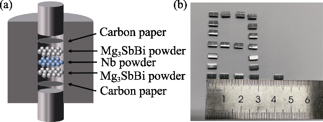
图1
Mg3SbBi/Nb/Mg3SbBi样品的(a)装样示意图和(b)粒子实物照片
Fig. 1
(a) Loading diagram and (b) physical particle picture of Mg3SbBi/Nb/Mg3SbBi sample
1.2 加速老化实验
将切割完成的Mg3SbBi/Nb/Mg3SbBi粒子真空封装(MRVS-202, Partulob)在石英玻璃管中, 置于退火炉(上海意丰)中以10 ℃/min速率升温至525 ℃恒温加速老化实验, 老化时间分别为70、170和360 h。每个时间点至少3个平行样品。
1.3 测试与表征
实验采用X射线衍射仪(DX-2700B, HAOYU-AN, CuKα)测试Mg3.2SbBi0.996Se0.004粉体与块体样品物相。测试角度范围2θ=10°~90°, 步进角度0.03°。采用热电性能测试系统(ZEM-3, ULVAC-RIKO)获得材料电导率σ、塞贝克系数S。采用阿基米德排水法测试样品密度ρ(g·cm-3); 采用激光热导仪(LFA-467, Netzsch)测试样品热扩散系数D(m2·s-1); 采用理论公式[22]计算样品比热容Cp(J·kg-1·K-1), 通过公式κ = CpDρ计算热导率。最终计算材料的热电优值ZT= S2Tκ。
用粒径1.25 μm (7000目)砂纸抛光Mg3SbBi/Nb/Mg3SbBi “三明治”粒子, 利用热场发射扫描电镜(TESCAN MAIA 3, Czech republic)观察界面微观形貌, 搭配能谱仪(QUANTAX EDS XFlash7, BRUKER, 加速电压15 kV)定量分析界面元素成分含量。利用自搭建的界面电阻率测试仪, 基于文献[23]报道的四探针法测试样品界面电阻率, 步进角5 μm。多次测试各个样品表面的不同位置, 取平均值。
2 结果与讨论
2.1 Mg3SbBi物相成分表征与热电性能研究
图2
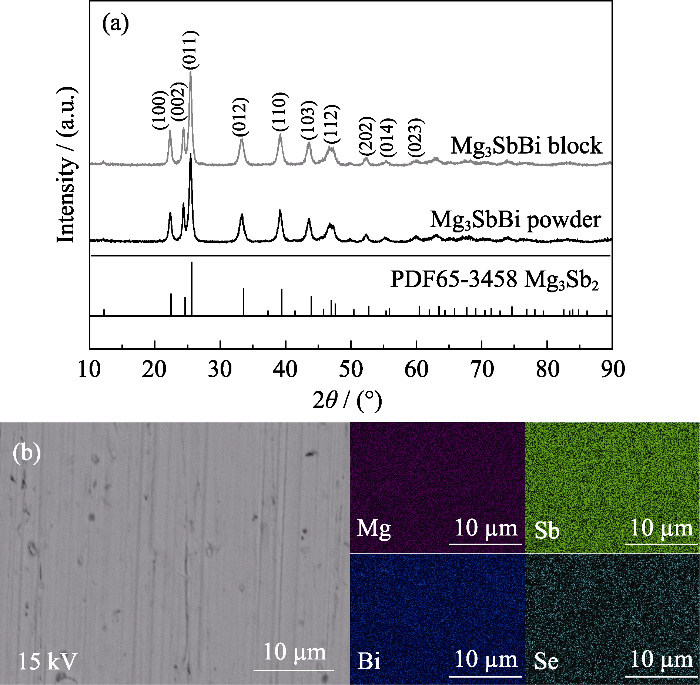
图2
Mg3SbBi样品的(a)粉体与块体XRD衍射图谱和(b)块体面扫描元素分布图
Fig. 2
(a) Powder and bulk XRD patterns and (b) block decent scanning element distribution mappings of Mg3SbBi sample
图3给出了不同保温时间条件下热压烧结制备Mg3.2SbBi0.996Se0.004样品的热电性能。随着保温时间延长, 样品的室温电导率逐渐增大(图3(a)), 这是因为晶粒尺寸越小晶界相散射作用越明显[24], 延长保温时间可促进晶粒长大, 减弱晶界相散射对材料电导率的影响[25]。样品的塞贝克系数随烧结时间延长变化不大(图3(b)), 进一步验证了样品的低温电导率升高是由于晶界相散射减弱导致的载流子迁移率升高, 而非载流子浓度的变化。不同保温时间对样品的晶格热导率影响不大, 如图3(c)所示。最终, 如图3(d)所示, 750 ℃热压烧结15 min的样品最大ZT可以达到1.4(测试温度327 ℃)。
图3
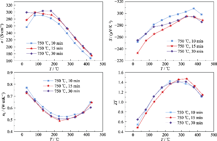
图3
热压750 ℃热压烧结不同时间的样品的热电性能随测试温度的变化曲线
Fig. 3
Thermoelectric properties of hot-pressed 750 ℃ sintered samples with various holding time as a function of test temperature
(a) Electrical conductivity; (b) Seebeck coefficient; (c) Lattice thermal conductivity; (d) ZT
2.2 Mg3SbBi/Nb/Mg3SbBi界面微观形貌与成分研究
图4给出了经过750 ℃热压烧结(Hot Pressing, HP)15 min、切割并抛光得到 “三明治”结构样品界面扫描电镜分析结果, 其中图4(a)方框位置放大对应图4(b, c)。图4(a, c)中, Nb阻挡层中心位置存在少量Mg-Sb/Bi成分和孔洞。阻挡层含有Mg-Sb/Bi成分应该是在装料过程中Mg3SbBi颗粒混入Nb粉所导致的。孔洞是因为750 ℃的烧结温度还不足以使Nb粉完全烧结致密所致。从图4(b)发现, Nb阻挡层和基体界面处均连接良好, 无裂纹和孔洞, 也未生成第二相。这表明Nb粉在烧结过程中与Mg3SbBi基体存在一定的扩散连接, 与之前报道的高通量筛选结果一致[13]。图4(c)区域的EDS(Energy Disperse Spectroscopy)扫描结果(表1)中, Nb阻挡层中心位置偏离Mg3SbBi化学计量比, 其中Sb元素含量明显降低, 而Bi含量增加, 但Mg元素与Sb、Bi元素之和的比例仍旧保持约3:2, 如表1所示。
图4
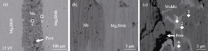
图4
老化前Mg3SbBi/Nb/Mg3SbBi样品的(a)背散射电子图和(b, c)图(a)中相应区域的放大图
Fig. 4
(a) BSE image of Mg3SbBi/Nb/Mg3SbBi sample before aging and (b, c) magnified images of corresponding areas in (a)
表1
Table 1
| Point | Mg/% | Sb/% | Bi/% | Nb/% |
|---|---|---|---|---|
| 1 | 59.75 | 9.25 | 29.64 | 1.36 |
| 2 | 51.88 | 8.35 | 25.57 | 14.20 |
| 3 | 1.19 | 0.14 | 0.13 | 98.54 |
| 4 | 58.78 | 19.85 | 20.22 | 1.15 |
图5是封装玻璃管样品在525 ℃分别老化70、160、360 h背散射分析结果。图5(a~c)中, Nb阻挡层表面的Mg3SbBi组分偏析产生了孔洞与微裂纹。随老化时间延长, 孔洞连接延展形成纵向裂纹。推测原因是在老化过程中Nb阻挡层中组分偏析的Mg3SbBi更易发生Mg挥发, 导致孔洞产生。随老化时间延长孔洞增多, 并且由于升降温过程中产生热应力导致形成裂纹。525 ℃老化360 h样品(图5(c))的界面处存在单质Bi, 由于Mg3SbBi侧材料本身无明显结构破坏, 推测单质Bi来自Nb阻挡层中心位置成分偏析的基体。图5(d~f)是砂纸打磨抛光后样品的BSE(Backscattered Electron)照片,从图中看出, Nb阻挡层已没有裂纹, 与基体界面处连接良好, 这说明Nb阻挡层中心位置的裂纹是由Mg3SbBi基体组分偏析、成分缺失导致, 并且开裂由表及里逐渐扩展, 所以避免Mg3SbBi颗粒混入Nb阻挡层可以减少Nb层中产生的裂纹, 延长服役时间。
图5
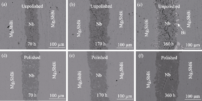
图5
Mg3SbBi/Nb/Mg3SbBi结构在525 ℃老化70、160、360 h的背散射电子照片
Fig. 5
BSE images of the interface of Mg3SbBi/Nb/Mg3SbBi after aging at 525 ℃ for 70, 160 and 360 h
(a-c) Before polished; (d-f) After polished
图6给出了经过525 ℃老化不同时间并抛光后样品表面的EDS线扫描结果, 表征相应元素浓度随扫描线位移的变化关系。老化过程中Nb/Mg3SbBi界面处无明显的元素扩散, 并且没有产生裂纹和孔洞, 界面扩散层厚度随老化时间延长增加缓慢, 这说明在525 ℃恒温老化服役过程中Nb阻挡层与Mg3SbBi基体之间的界面保持良好的化学稳定性。
图6
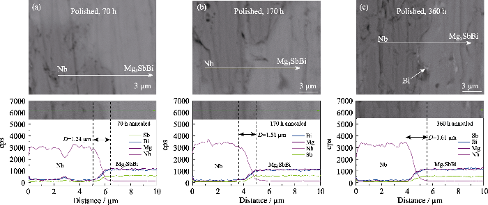
图6
Nb/Mg3SbBi界面525 ℃老化不同时间的背散射电子图(上)和线扫描结果(下)
Fig. 6
Backscatter (up) and line sweep (down) results of Nb /Mg3SbBi interface aged at 525℃for different time
(a) 70; (b) 170 h; (c) 360 h; Colorful figures are available on website
2.3 Mg3SbBi/Nb/Mg3SbBi界面电阻率演变
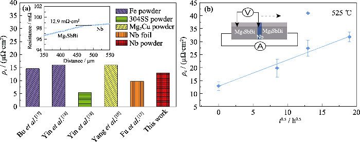
图7是Nb阻挡层界面电阻率随老化时间的变化结果。从图7(a)可以看出, Nb/Mg3SbBi界面初始电阻率为12.9 μΩ·cm2,与目前文献报道的Fe[17-18] (~15 μΩ·cm2)、304不锈钢[18](~6 μΩ·cm2)、Mg2Cu[19] (~11 μΩ cm2)、Nb箔[13](~10 μΩ cm2)等阻挡层材料的电阻率大小相近。经历525 ℃老化70、170和360 h后, 界面电阻率分别增大至19.8、27.4和31.8 μΩ·cm2。拟合界面电阻率随老化时间的变化关系后发现, 界面电阻率与老化时间的平方根呈线性关系, 如图7(b)所示, 表现出扩散主导的变化规律[26], 这与图(5)和图(6)的结果一致。总之, 虽然长时间老化导致界面处元素发生微弱扩散, 但是Nb阻挡层的性能仍较为优异。
图7
3 结论
本研究首先探索了750 ℃, 50 MPa下保温10、15和30 min的Mg3SbBi热电材料性能, 发现随保温时间延长, 其低温区热电性能有所提升, 样品在300 ℃最大ZT可达1.4。然后选择Nb粉作为阻挡层, 热压烧结制备了Mg3SbBi/Nb/Mg3SbBi “三明治”样品, 并在525 ℃进行70 、170及 360 h加速老化试验, 系统研究了界面层的组成、微结构以及电阻率随老化时间的演变过程。Nb粉阻挡层混入的Mg3SbBi颗粒在烧结过程挥发导致产生孔洞。在老化过程中, Nb粉阻挡层表层孔洞延展形成纵向裂纹, 表面抛光后, 内部无明显变化。老化前后, Nb/Mg3 SbBi界面均连接良好, 无第二相生成, 扩散层厚度随老化时间延长缓慢增加至1.6 μm。界面电阻率从初始的12.9 μΩ·cm2增加到19.8、27.4和31.8 μΩ·cm2, 与老化时间的平方根呈线性关系, 表现出扩散主导的变化规律。因此, 对于Mg3(Sb,Bi)2基热电材料器件, 选择具备微弱界面扩散且结构致密的Nb作为阻挡层材料, 服役过程中可以有效阻挡Mg、Sb元素扩散, 有利于提升器件的稳定性和可靠性。
参考文献
Preparation and characterization of Ag2Se-based ink used for inkjet printing
In-situ growth of carbon nanotubes on ZnO to enhance thermoelectric and mechanical properties

As a high-temperature thermoelectric (TE) material, ZnO offers advantages of non-toxicity, chemical stability, and oxidation resistance, and shows considerable promise as a true ready-to-use module under air conditions. However, poor electrical conductivity and high thermal conductivity severely hinder its application. Carbon nanotubes (CNTs) are often used as a reinforcing phase in composites, but it is difficult to achieve uniform dispersion of CNTs due to van der Waals forces. Herein, we developed an effective in-situ growth strategy of homogeneous CNTs on ZnO nanoparticles by exploiting the chemical vapor deposition (CVD) technology, in order to improve their electrical conductivity and mechanical properties, as well as reducing the thermal conductivity. Meanwhile, magnetic nickel (Ni) nanoparticles are introduced as catalysts for promoting the formation of CNTs, which can also enhance the electrical and thermal transportation of ZnO matrices. Notably, the electrical conductivity of ZnO is significantly boosted from 26 to 79 S·cm−1 due to the formation of dense and uniform conductive CNT networks. The lattice thermal conductivity (κL) is obviously declined by the intensification of phonon scattering, resulting from the abundant grain boundaries and interfaces in ZnO-CNT composites. Importantly, the maximum dimensionless figure of merit (zT) of 0.04 at 800 K is obtained in 2.0% Ni-CNTs/ZnO, which is three times larger than that of CNTs/ZnO prepared by traditional ultrasonic method. In addition, the mechanical properties of composites including Vickers hardness (HV) and fracture toughness (KIC) are also reinforced. This work provides a valuable reference for dispersing nano-phases in TE materials to enhance both TE and mechanical properties.
Elevated temperature behavior of CuPb18SbTe20/nano-Ag/Cu joints for thermoelectric devices
Interfacial reactions between PbTe-based thermoelectric materials and Cu and Ag bonding materials
Realizing a thermoelectric conversion efficiency of 12% in bismuth telluride/skutterudite segmented modules through full-parameter optimization and energy-loss minimized integration
Thermoelectric interface materials: a perspective to the challenge of thermoelectric power generation module
Technologies and applications of thermoelectric devices: current status, challenges and prospects
Thermoelectric device: contact interface and interface materials
Isotropic conduction network and defect chemistry in Mg3+δSb2-based layered Zintl compounds with high thermoelectric performance
Discovery of high-performance low-cost n-type Mg3Sb2-based thermoelectric materials with multi-valley conduction bands
Widespread application of thermoelectric devices for waste heat recovery requires low-cost high-performance materials. The currently available n-type thermoelectric materials are limited either by their low efficiencies or by being based on expensive, scarce or toxic elements. Here we report a low-cost n-type material, Te-doped Mg3Sb1.5Bi0.5, that exhibits a very high figure of merit zT ranging from 0.56 to 1.65 at 300−725 K. Using combined theoretical prediction and experimental validation, we show that the high thermoelectric performance originates from the significantly enhanced power factor because of the multi-valley band behaviour dominated by a unique near-edge conduction band with a sixfold valley degeneracy. This makes Te-doped Mg3Sb1.5Bi0.5 a promising candidate for the low- and intermediate-temperature thermoelectric applications.
Research progress on crystal growth and the thermoelectric properties of Zintl phase Mg3X2(X=Sb, Bi) based materials
Application of entropy engineering in thermoelectrics
Mg3(Bi,Sb)2-based thermoelectric modules for efficient and reliable waste-heat utilization up to 750 K
Suppression of interfacial diffusion in Mg3Sb2 thermoelectric materials through an Mg4.3Sb3Ni/Mg3.2Sb2Y0.05/Mg4.3Sb3Ni-graded structure
Realizing high conversion efficiency of Mg3Sb2-based thermoelectric materials
High thermoelectric energy conversion efficiency of a unicouple of n-type Mg3Bi2 and p-type Bi2Te3
An over 10% module efficiency obtained using non-Bi2Te3 thermoelectric materials for recovering heat of <600 K
Reliable N-type Mg3.2Sb1.5Bi0.49Te0.01/304 stainless steel junction for thermoelectric applications
Next-generation thermoelectric cooling modules based on high-performance Mg3(Bi,Sb)2 material
Interfacial behaviors of p-type CeyFexCo4-xSb12/Nb thermoelectric joints
Interfacial stress analysis on skutterudite-based thermoelectric joints under service conditions
Heat capacity of Mg3Sb2, Mg3Bi2, and their alloys at high temperature
Design of apparatus for Ni/Mg2Si and Ni/MnSi1.75 contact resistance determination for thermoelectric legs
Grain boundary dominated charge transport in Mg3Sb2-based compounds
Improvement of low-temperature ZT in a Mg3Sb2-Mg3Bi2 solid solution via Mg-vapor annealing
Electrode interface optimization advances conversion efficiency and stability of thermoelectric devices
Although the CoSb3-based skutterudite thermoelectric devices have been highly expected for wide uses such as waste heat recovery and space power supply, the limited long-term service stability majorly determined by the degradation of electrode interface obstructs its applications. Here, we built up an effective criterion for screening barrier layer based on the combination of negative interfacial reaction energy and high activation energy barrier of Sb migration through the formed interfacial reaction layer. Accordingly, we predicted niobium as a promising barrier layer. The experimental results show the skutterudite/Nb joint has the slowest interfacial reaction layer growth rate and smallest interfacial electrical resistivity. The fabricated 8-pair skutterudite module using Nb as barrier layer achieves a recorded conversion efficiency of 10.2% at hot-side temperature of 872 K and shows excellent stability during long-time aging. This simple criterion provides an effective guidance on screening barrier layer with bonding-blocking-conducting synergetic functions for thermoelectric device integration.
