Journal of Inorganic Materials ›› 2024, Vol. 39 ›› Issue (3): 283-290.DOI: 10.15541/jim20230476
Special Issue: 【信息功能】功能晶体(202512)
• RESEARCH ARTICLE • Previous Articles Next Articles
YANG Zhiliang1( ), YANG Ao1, LIU Peng1, CHEN Liangxian1, AN Kang2, WEI Junjun1, LIU Jinlong1, WU Lishu3(), LI Chengming1()
Received:2023-10-16
Revised:2023-11-12
Published:2024-03-20
Online:2023-12-04
Contact:
WU Lishu, senior engineer. E-mail: wulishu117@163.com;About author:YANG Zhiliang (1994-), male, PhD candidate. E-mail: 1220715584@qq.com
Supported by:CLC Number:
YANG Zhiliang, YANG Ao, LIU Peng, CHEN Liangxian, AN Kang, WEI Junjun, LIU Jinlong, WU Lishu, LI Chengming. Preparation of 3-inch Diamond Film on Silicon Substrate for Thermal Management[J]. Journal of Inorganic Materials, 2024, 39(3): 283-290.
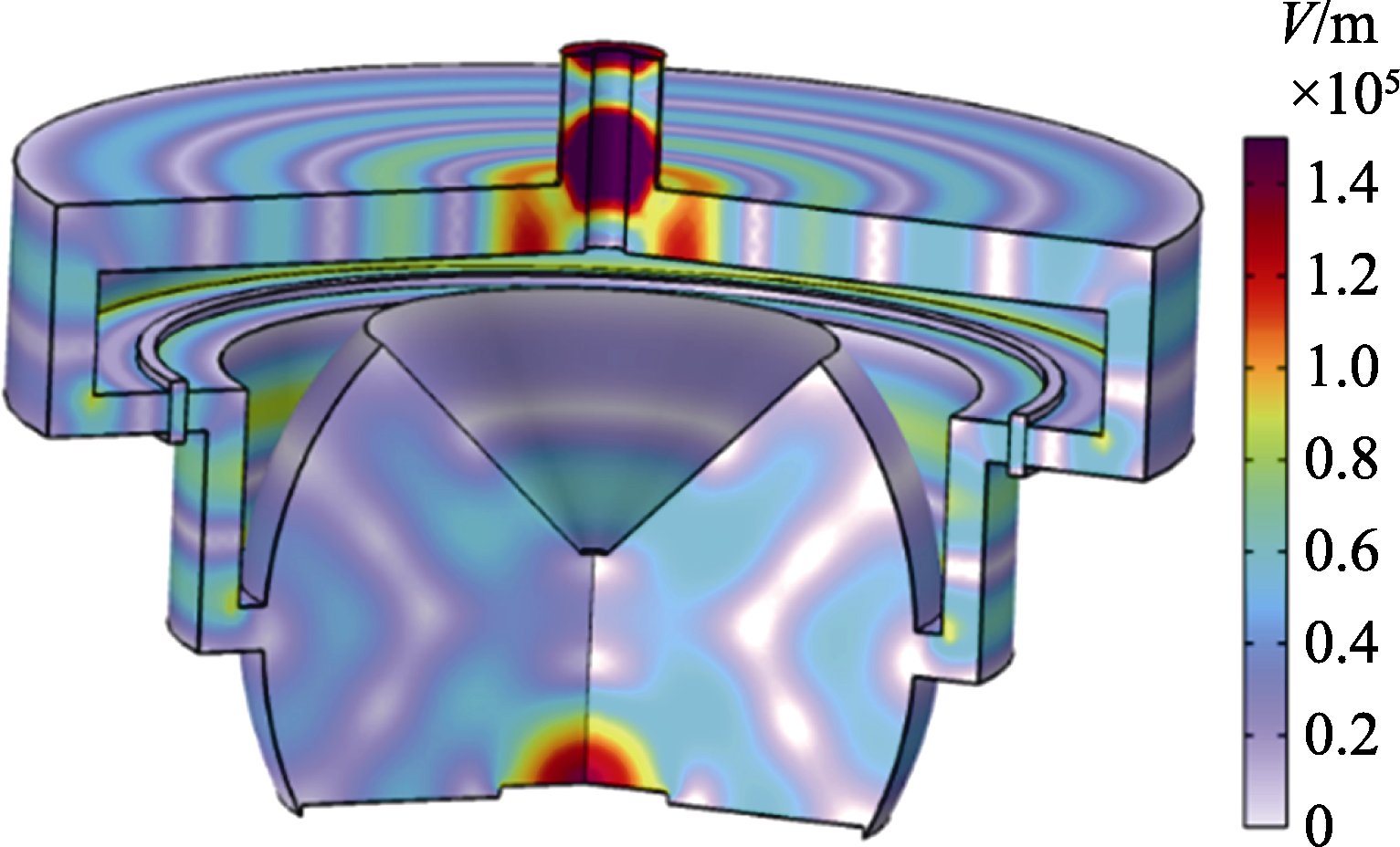
Fig. 1 Three-dimensional resonance mode diagram of microwave electric field in MPCVD device
| Num. | Electron collision reaction | Collision type | Energy loss/eV |
|---|---|---|---|
| 1 | Elastic collision | - | |
| 2 | Excitation | 14 | |
| 3 | Dissociation | 8.9 | |
| 4 | Ionization | 15.4 |
Table 1 Set of collision reactions [21]
| Num. | Electron collision reaction | Collision type | Energy loss/eV |
|---|---|---|---|
| 1 | Elastic collision | - | |
| 2 | Excitation | 14 | |
| 3 | Dissociation | 8.9 | |
| 4 | Ionization | 15.4 |
| Num. | Surface reaction | Adhesion factor | Secondary emission coefficient |
|---|---|---|---|
| 1 | 1 | 0 | |
| 2 | 1 | 0 | |
| 3 | 1 | 0 |
Table 2 Collection of surface reactions
| Num. | Surface reaction | Adhesion factor | Secondary emission coefficient |
|---|---|---|---|
| 1 | 1 | 0 | |
| 2 | 1 | 0 | |
| 3 | 1 | 0 |
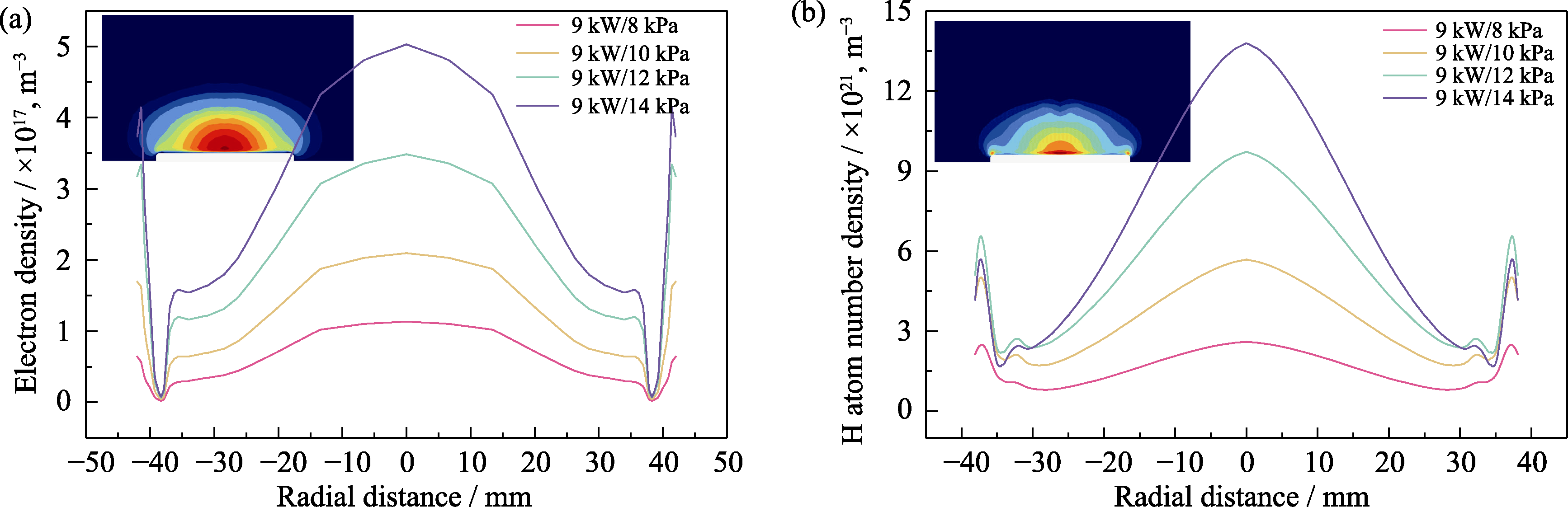
Fig. 2 Group distribution in the axial direction of the reactor under different microwave power/chamber pressure conditions (a) Electron number density distribution; (b) Atomic H number density distribution
| Chamber pressure/kPa | ne/m−3 | nH/m−3 | ||
|---|---|---|---|---|
| r=0, z=0.5 | r=38.1, z=0.5 | r=0, z=0.5 | r=38.1, z=0.5 | |
| 6 | 1.14×10¹⁷ | 1.96×10¹⁵ | 2.83×10²¹ | 1.26×10²¹ |
| 8 | 2.09×10¹⁷ | 3.18×10¹⁵ | 6.00×10²¹ | 2.02×10²¹ |
| 10 | 3.44×10¹⁷ | 4.63×10¹⁵ | 1.05×10²² | 2.21×10²¹ |
| 12 | 4.97×10¹⁷ | 5.31×10¹⁵ | 1.51×10²² | 1.67×10²¹ |
Table 3 Electron number density ne and atomic H number density nH at the center (r=0, z=0.5) and edge (r=38.1, z=0.5) of the substrate under different chamber pressures
| Chamber pressure/kPa | ne/m−3 | nH/m−3 | ||
|---|---|---|---|---|
| r=0, z=0.5 | r=38.1, z=0.5 | r=0, z=0.5 | r=38.1, z=0.5 | |
| 6 | 1.14×10¹⁷ | 1.96×10¹⁵ | 2.83×10²¹ | 1.26×10²¹ |
| 8 | 2.09×10¹⁷ | 3.18×10¹⁵ | 6.00×10²¹ | 2.02×10²¹ |
| 10 | 3.44×10¹⁷ | 4.63×10¹⁵ | 1.05×10²² | 2.21×10²¹ |
| 12 | 4.97×10¹⁷ | 5.31×10¹⁵ | 1.51×10²² | 1.67×10²¹ |
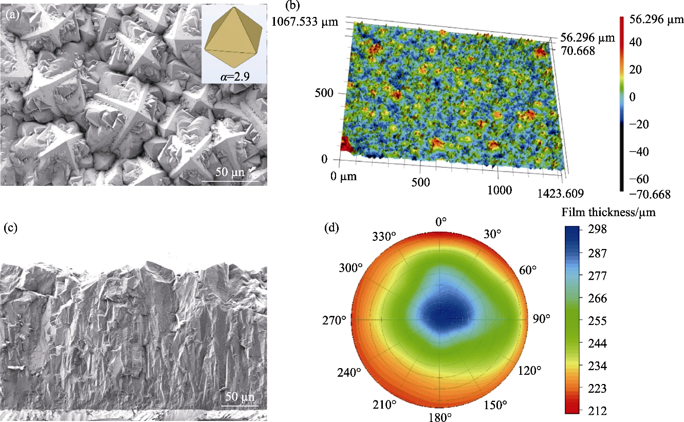
Fig. 3 Surface morphology, cross-sectional morphology and thickness distribution of the diamond film (a) Surface topography of a silicon substrate diamond film with inset illustrating the ideal diamond crystal profile when the growth parameter α is 2.9; (b) Surface profile of silicon substrate diamond film obtained by laser confocal microscope; (c) Cross-sectional morphology of the edge of the diamond film; (d) Thickness distribution of diamond film
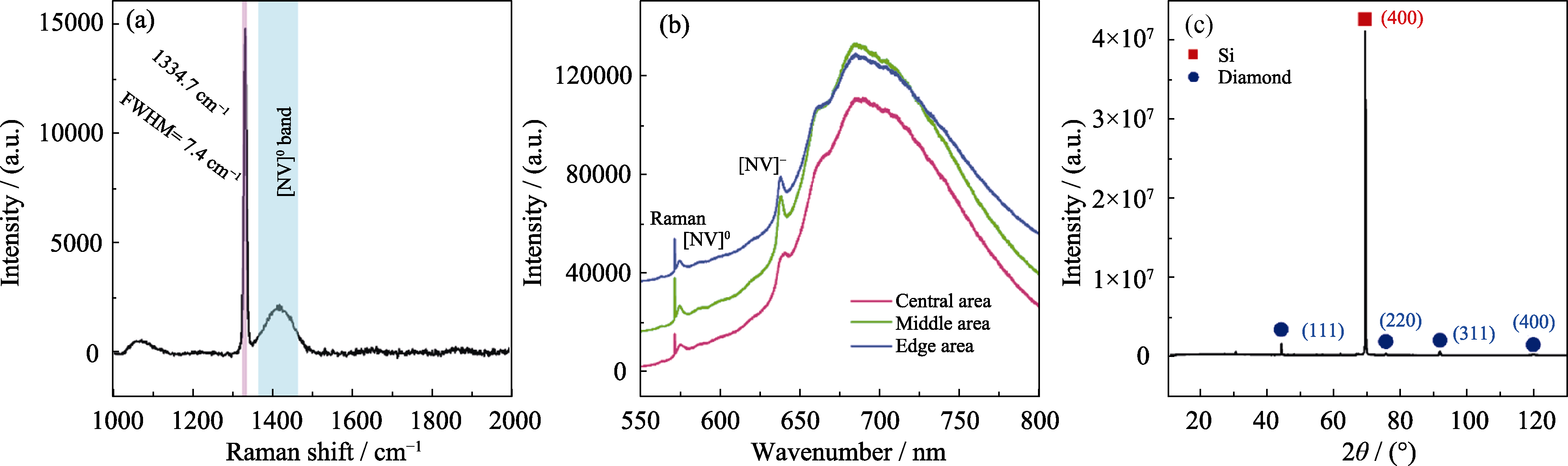
Fig. 4 Raman spectrum (a), PL spectra (b) and XRD pattern (c) of diamond films on silicon substrate
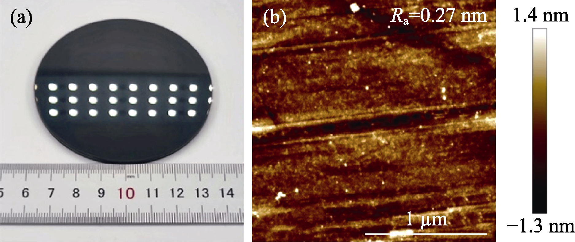
Fig. 5 Actual photographic and AFM morphology of polished diamond films on silicon substrate (a) Actual photographic; (b) AFM image
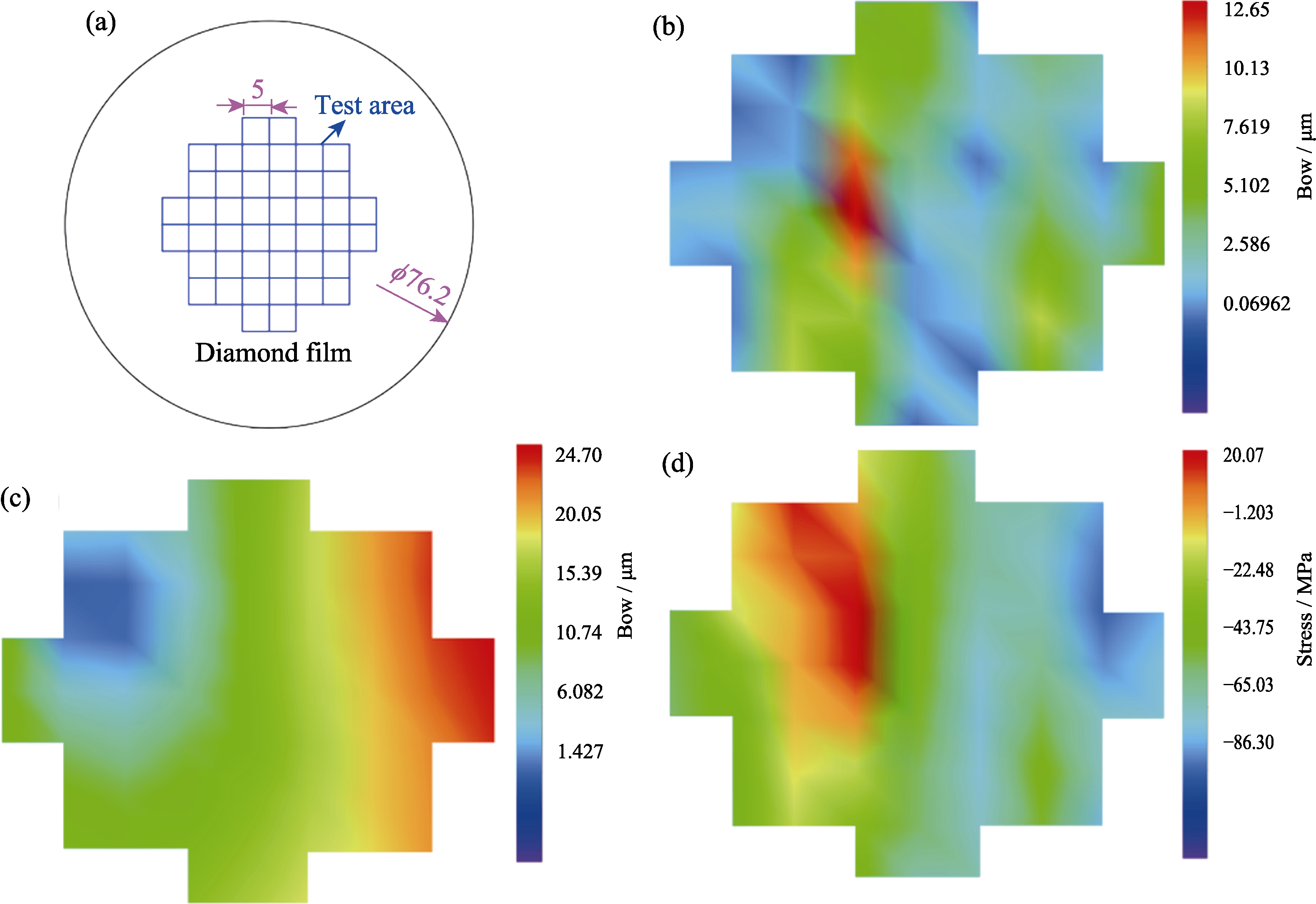
Fig. 6 Results of film bending and stress test (a) Test area of the film stress test system; (b) Bending test results of the monocrystalline silicon substrate; (c) Bending test results of the polished silicon substrate diamond film; (d) Internal stress of the diamond film calculated by the Stoney formula
| [1] |
PEARTON S J, REN F, ZHANG A P, et al. Fabrication and performance of GaN electronic devices. Mater. Sci. Engin.: R: Reports, 2000, 30(3-6): 55.
DOI URL |
| [2] | MAZUMDER S K, VOSS L F, DOWLING K, et al. Overview of wide/ultra-wide bandgap power semiconductor devices for distributed energy resources. IEEE J. Em. Sel. Top. P., 2023, 11(4): 3957. |
| [3] |
AJAYAN J, NIRMAL D, RAMESH R, et al. A critical review of AlGaN/GaN-heterostructure based Schottky diode/HEMT hydrogen (H2) sensors for aerospace and industrial applications. Measurement, 2021, 186: 110100.
DOI URL |
| [4] |
NUTTINCK S, GEBARA E, LASKAR J, et al. Study of self-heating effects, temperature-dependent modeling, and pulsed load- pull measurements on GaN HEMTs. IEEE T. Microw. Theory., 2001, 49(12): 2413.
DOI URL |
| [5] |
QIN Y, CHAI C, LI F, et al. Study of self-heating and high-power microwave effects for enhancement-mode p-gate GaN HEMT. Micromachines, 2022, 13(1): 106.
DOI URL |
| [6] |
CHEN J T, BERGSTEN J, LU J, et al. A GaN-SiC hybrid material for high-frequency and power electronics. Appl. Phys. Lett., 2018, 113(4): 041605.
DOI URL |
| [7] |
CHEN K J, HABERLEN O, LIDOW A, et al. GaN-on-Si power technology: devices and applications. IEEE T. Electron. Dev., 2017, 64(3): 779.
DOI URL |
| [8] |
MIZUE C, HORI Y, MICZEK M, et al. Capacitance-voltage characteristics of Al2O3/AlGaN/GaN structures and state density distribution at Al2O3/AlGaN interface. Jpn. J. Appl. Phys., 2011, 50(2R): 021001.
DOI |
| [9] |
LIU H, LI J, LI Z, et al. Single crystal diamond deposited by dual radio-frequency plasma jet CVD with high growth rate. Crystals, 2019, 9(1): 32.
DOI URL |
| [10] |
ZUO Y, LI J, BAI Y, et al. Growth of nanocrystalline diamond by dual radio frequency inductively coupled plasma jet CVD. Diam. Relat. Mater., 2017, 73: 67.
DOI URL |
| [11] | POMEROY J, BERNARDONI M, SARUA A, et al. Achieving the best thermal performance for GaN-on-diamond. 2013 IEEE Compound Semiconductor Integrated Circuit Symposium (CSICS), 2013, 1: 6659210. |
| [12] | ZHAO J, HAO X, ZHAO K, et al. Recent development on high thermal conductivity diamond synthesized by microwave plasma chemical vapor deposition and its devices applications. J. Chin. Ceram. Soc., 2022, 50(7): 1852. |
| [13] |
GROTJOHN T, LISKE R, HASSOUNI K, et al. Scaling behavior of microwave reactors and discharge size for diamond deposition. Diam. Relat. Mater., 2005, 14(3-7): 288.
DOI URL |
| [14] |
SILVA F, BONNIN X, SCHARPF J, et al. Microwave analysis of PACVD diamond deposition reactor based on electromagnetic modelling. Diam. Relat. Mater., 2010, 19(5/6): 397.
DOI URL |
| [15] |
LI Y F, SU J J, LIU Y Q, et al. A circumferential antenna ellipsoidal cavity type MPCVD reactor developed for diamond film deposition. Diam. Relat. Mater., 2015, 51: 24.
DOI URL |
| [16] |
AN K, ZHANG S, SHAO S, et al. Effects of the electric field at the edge of a substrate to deposit a ϕ100 mm uniform diamond film in a 2.45 GHz MPCVD system. Plasma Sci. Technol., 2022, 24(4): 045502.
DOI |
| [17] |
WENG J, LIU F, XIONG L W, et al. Deposition of large area uniform diamond films by microwave plasma CVD. Vacuum, 2018, 147: 134.
DOI URL |
| [18] |
LI Y C, LIU X D, HAO X B, et al. Rapid growth of single crystal diamond at high energy density by plasma focusing. J. Inorg. Mater., 2023, 38(3): 303.
DOI |
| [19] |
YAMADA H, CHAYAHARA A, MOKUNO Y. Simplified description of microwave plasma discharge for chemical vapor deposition of diamond. J. Appl. Phys., 2007, 101(6): 063302.
DOI URL |
| [20] |
SU J J, LI Y F, LI X L, et al. A novel microwave plasma reactor with a unique structure for chemical vapor deposition of diamond films. Diam. Relat. Mater., 2014, 42: 28.
DOI URL |
| [21] | Itikawa database. www.lxcat.net.(2022-04-10)[2023-11-08]. |
| [22] |
YANG D, GUO L, WANG B, et al. Hydrogen plasma characteristics in a microwave chemical vapor deposition chamber. Mater. Sci. Eng. B-Adv., 2023, 292: 116422.
DOI URL |
| [23] |
MESBAHI A, SILVA F, FARHAT S, et al. Hydrodynamics effects in high power density microwave plasma diamond growth reactors. J. Phys. D Appl. Phys., 2013, 46(38): 385502.
DOI URL |
| [24] | ZHANG S, AN K, SHAO S W, et al. Microwave power and deposition pressure matching of MPCVD diamond films. J. Synth. Cryst., 2022, 51(5): 910. |
| [25] |
WILD C, KOIDL P, MULLER-SEBERT W, et al. Chemical vapour deposition and characterization of smooth {100}-faceted diamond films. Diam. Relat. Mater., 1993, 2(2/3/4): 158.
DOI URL |
| [26] | ZHU H X, WU S, HUANG L L, et al. Effect of methane concentration on twins in CVD polycrystalline diamond film. Physics Examination and Testing, 2014, 32(1): 7. |
| [27] | MAO W M, ZHU H X, CHEN L, et al. Macro-texture and micro-twinning in CVD free-standing diamond films. J. Inorg. Mater., 2006, 21(1): 239. |
| [28] |
LEIGH W G S, CUENCA J A, THOMAS E L H, et al. Mapping the effect of substrate temperature inhomogeneity during microwave plasma-enhanced chemical vapour deposition nanocrystalline diamond growth. Carbon, 2023, 201: 328.
DOI URL |
| [29] |
HUAMH Y, ROSAKIS A J. Extension of Stoney's formula to non-uniform temperature distributions in thin film/substrate systems. The case of radial symmetry. J. Mech. Phys. Solids., 2005, 53(11): 2483.
DOI URL |
| [30] | NAKAMURA Y, SAKAGAMI S, AMAMOTO Y, et al. Measurement of internal stresses in CVD diamond films. Thin Solid Films, 1997, 308: 249. |
| [31] |
LI X, LI C, GAO C, et al. Internal stress in MPCVD diamond films on the Si substrate based on XRD line shape. Optoelectron. Lett., 2009, 5(4): 273.
DOI URL |
| [32] |
LI H Y, KUANG F H, WU H L, et al. Temperature dependence of residual tensile stresses and its influences on crack propagation behaviour. J. Inorg. Mater., 2023, 38(11): 1265.
DOI URL |
| [1] | LI Yicun, LIU Xuedong, HAO Xiaobin, DAI Bing, LYU Jilei, ZHU Jiaqi. Rapid Growth of Single Crystal Diamond at High Energy Density by Plasma Focusing [J]. Journal of Inorganic Materials, 2023, 38(3): 303-309. |
| [2] | LI Yicun, HAO Xiaobin, DAI Bing, WEN Dongyue, ZHU Jiaqi, GENG Fangjuan, YUE Weiping, LIN Weiqun. Optimization Design of MPCVD Single Crystal Diamond Growth Based on Plasma Diagnostics [J]. Journal of Inorganic Materials, 2023, 38(12): 1405-1412. |
| [3] | CHAN Siyi, TU Juping, HUANG Ke, SHAO Siwu, YANG Zhiliang, LIU Peng, LIU Jinlong, CHEN Liangxian, WEI Junjun, AN Kang, ZHENG Yuting, LI Chengming. Uniform Growth of Two-inch MPCVD Optical Grade Diamond Film [J]. Journal of Inorganic Materials, 2023, 38(12): 1413-1419. |
| [4] | SU Jing-Jie, YANG Zi, LI Yi-Feng, TANG Wei-Zhong, AN Xiao-Ming, GUO Hui. Measurement of Microwave Dielectric Properties of Diamond Films Using Split-cylinder Resonator Method [J]. Journal of Inorganic Materials, 2015, 30(7): 751-756. |
| [5] | QIU Wan-Qi, PAN Jian-Wei, LIU Zhong-Wu, YU Hong-Ya, ZHONG Xi-Chun, ZENG De-Chang. Improvement of Adhesive Strength of Diamond Films by Plating Cr-diamond Composite Interlayer [J]. Journal of Inorganic Materials, 2012, 27(2): 205-208. |
| [6] | LIU Jin-Long, LI Cheng-Ming, CHEN Liang-Xian, HEI Li-Fu, LV Fan-Xiu. Progress of High Frequency and High Output Power FET [J]. Journal of Inorganic Materials, 2010, 25(9): 897-905. |
| [7] | SHEN Hu-Jang,WANG Lin-Jun,HUANG Jian,XU Run,SHI Wei-Ming,XIA Yi-Ben. Research for (100)-Oriented Diamond Film Radiation Detector [J]. Journal of Inorganic Materials, 2009, 24(6): 1254-1258. |
| [8] | ZHU Hong-Xi,MAO Wei-Min,FENG Hui-Ping,LU Fan-Xiu,Vlasov I I,Ralchenko V G,Khomich A V. Influence of Methane Concentration on Crystal Growing Process in CVD Free Standing Diamond Films [J]. Journal of Inorganic Materials, 2007, 22(3): 570-576. |
| [9] | WU Nan-Chun,XIA Yi-Ben,TAN Shou-Hong,LIU Jian-Min,SU Qing-Feng,WANG Lin-Jun. Influences of Positive Bias on Microstructure and Electrical Properties of Nanocrystalline Diamond Films [J]. Journal of Inorganic Materials, 2007, 22(2): 381-384. |
| [10] | LIU Jian-Min,XIA Yi-Ben,WANG Lin-Jun,ZHANG Ming-Long,SU Qing-Feng. Effects of Process Conditions on Electric Properties of Hot-filament CVD Diamond Films [J]. Journal of Inorganic Materials, 2006, 21(4): 1018-1024. |
| [11] | SU Qing-Feng,XIA Yi-Ben,WANG Lin-Jun,SHI Wei-Min. Improvement Smoothness of CVD Diamond by Composite Polishing [J]. Journal of Inorganic Materials, 2006, 21(2): 499-502. |
| [12] | MAO Wei-Min,ZHU Hong-Xi,CHEN Leng,FENG Hui-Ping,LU Fan-Xiu. Macro-texture and Micro-twins in Free-standing Diamond Films [J]. Journal of Inorganic Materials, 2006, 21(1): 239-244. |
| [13] | LIU Wei-Ping,YU Qing-Xuan,TIAN Yu-Quan,LIAO Yuan,WANG Guan-Zhong,FANG Rong-Chuan. Effects of Boron Doping on the Growth Characteristic of Diamond Film [J]. Journal of Inorganic Materials, 2005, 20(5): 1270-1274. |
| [14] | LIN Liang-Wu,TANG Yuan-Hong,ZHU Li-Bing. Effects of Atomic Hydrogen on Growth of Nanodiamond Films [J]. Journal of Inorganic Materials, 2005, 20(5): 1263-1269. |
| [15] | YANG Shi-E,LU Zhan-Ling,FAN Zhi-Qin,YAO Ning,ZHANG Bing-Lin. Highly Adherent Diamond Film Deposited onto WC-Co Cemented Carbide Substrate [J]. Journal of Inorganic Materials, 2005, 20(1): 235-238. |
| Viewed | ||||||
|
Full text |
|
|||||
|
Abstract |
|
|||||