Journal of Inorganic Materials ›› 2026, Vol. 41 ›› Issue (4): 493-499.DOI: 10.15541/jim20250290
• RESEARCH ARTICLE • Previous Articles Next Articles
XU Hao1( ), GU Haitao1, WU Honghui1, YUE Xiaofei1, LIN Siqi1, JIN Min1,2()
Received:2025-07-13
Revised:2025-08-28
Published:2026-04-20
Online:2025-09-27
Contact:
JIN Min, professor. E-mail: jmaish@aliyun.comAbout author:XU Hao (1998-), male, Master candidate. E-mail: xnddream@126.com
Supported by:CLC Number:
XU Hao, GU Haitao, WU Honghui, YUE Xiaofei, LIN Siqi, JIN Min. Crystal Growth and Properties of Bi-doped InSe[J]. Journal of Inorganic Materials, 2026, 41(4): 493-499.
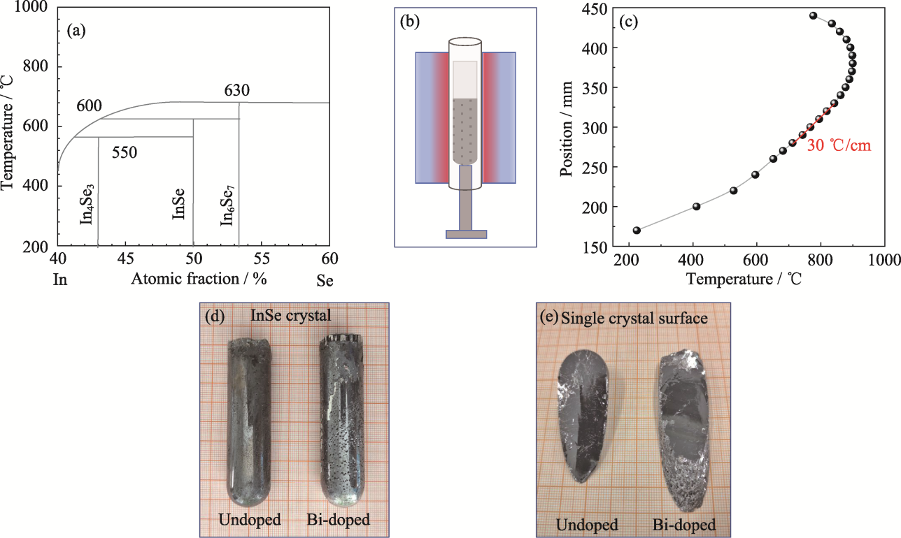
Fig. 1 InSe crystals growth (a) Two-dimensional phase diagram of In-Se; (b) Schematic diagram of the furnace for crucible descent method; (c) Furnace temperature profile for InSe crystal growth; (d) Optical image of the grown InSe crystals; (e) Optical image of the dissociation tablets of InSe corresponding to (d)
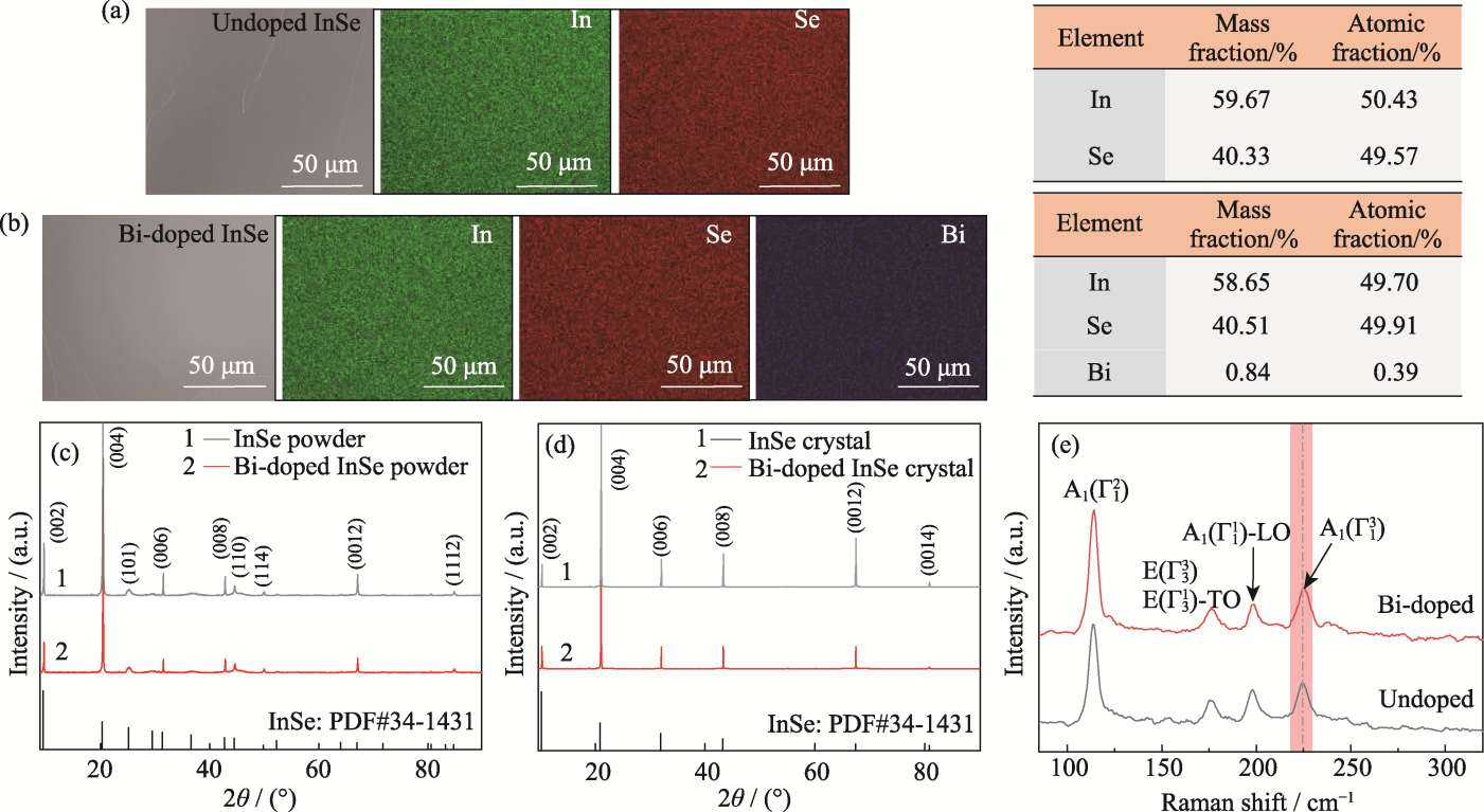
Fig. 2 Physical characterization of InSe crystals (a, b) SEM images and EDS analyses of (a) intrinsic InSe crystals and (b) Bi-doped InSe crystals; (c) Polycrystalline XRD patterns of InSe crystals; (d) Single crystal XRD patterns of InSe crystals; (e) Raman spectra of InSe crystals
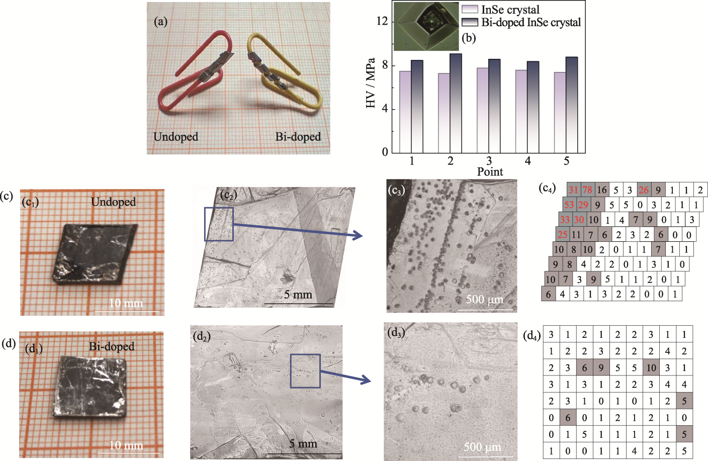
Fig. 3 Comparison of mechanical properties and chemical corrosion morphologies between undoped and Bi-doped InSe crystals (a) Macro-mechanical characterization of InSe crystals; (b) Mechanical comparison of InSe crystals under micro-hardness tester; (c, d) Dislocation density statistics of (c) intrinsic InSe crystal and (d) Bi-doped InSe crystal after corrosion. Colorful figures are available on website
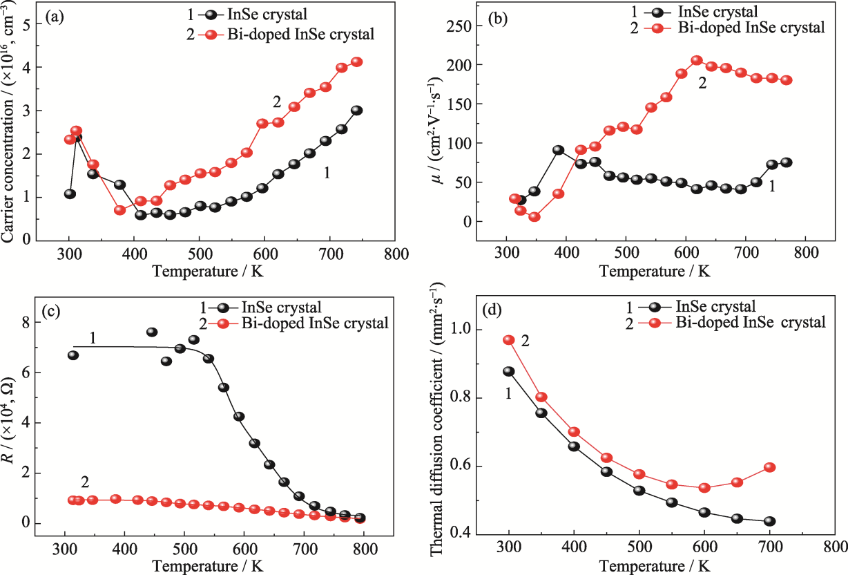
Fig. 4 Comparison of electrical and thermal properties between undoped and Bi-doped InSe crystals (a) Carrier concentration of InSe crystals; (b) Carrier mobility (μ) of InSe crystals; (c) Resistance (R) of InSe crystals; (d) Thermal diffusion coefficient of InSe crystals
| [1] |
JIANG J F, XU L, QIU C G, et al. Ballistic two-dimensional InSe transistors. Nature, 2023, 616(7957): 470.
DOI |
| [2] |
LEI S D, GE L H, NAJMAEI S, et al. Evolution of the electronic band structure and efficient photo-detection in atomic layers of InSe. ACS Nano, 2014, 8(2): 1263.
DOI PMID |
| [3] |
SUN R H, LIU Y, CHEN Y, et al. Efficient enhancement of photoluminescence and second-harmonic generation of few-layer InSe coupled with surface-plasmonic Ag prism array. Science China Materials, 2023, 66(7): 2788.
DOI |
| [4] |
WANG J J, CAO F F, JIANG L, et al. High-performance photodetectors of individual InSe single crystalline nanowire. Journal of the American Chemical Society, 2009, 131(43): 15602.
DOI URL |
| [5] |
DAI M J, GAO C F, NIE Q F, et al. Properties, synthesis, and device applications of 2D layered InSe. Advanced Materials Technologies, 2022, 7(12): 2200321.
DOI URL |
| [6] | 何峰, 白旭东, 陆欣昱, 等. III-VI族InSe半导体晶体生长研究进展. 人工晶体学报, 2022, 51(9): 1722. |
| [7] |
SUN M J, WANG W, ZHAO Q H, et al. ε-InSe single crystals grown by a horizontal gradient freeze method. CrystEngComm, 2020, 22(45): 7864.
DOI URL |
| [8] |
BANDURIN D A, TYURNINA A V, YU G L, et al. High electron mobility, quantum hall effect and anomalous optical response in atomically thin InSe. Nature Nanotechnology, 2017, 12(3): 223.
DOI PMID |
| [9] |
WEI T R, JIN M, WANG Y C, et al. Exceptional plasticity in the bulk single crystalline van der Waals semiconductor InSe. Science, 2020, 369(6503): 542.
DOI URL |
| [10] |
JIN M, MA Y P, WEI T R, et al. Growth and characterization of large size InSe crystal from non-stoichiometric solution via a zone melting method. Journal of Inorganic Materials, 2024, 39(5): 554.
DOI URL |
| [11] |
ZHAO L Y, JIANG Y J, LI C, et al. Probing anisotropic deformation and near-infrared emission tuning in thin-layered InSe crystal under high pressure. Nano Letters, 2023, 23(8): 3493.
DOI URL |
| [12] |
BAO X T, WU X X, KE Y X, et al. Giant out-of-plane exciton emission enhancement in two-dimensional indium selenide via a plasmonic nanocavity. Nano Letters, 2023, 23(9): 3716.
DOI URL |
| [13] | 郑权, 刘学超, 王浩, 等. 铝掺杂对硒化铟晶体结构与性能的影响. 人工晶体学报, 2024, 53(9): 1528. |
| [14] |
BENJAMIN H B, NIRMAL T, SHAJAN N, et al. Effect of Bi doping in tuning the structural, morphological and optoelectronic properties of solvothermal synthesized SnS nanorods. Materials Today Communications, 2024, 39: 109041.
DOI URL |
| [15] |
SUI F R, JIN M, ZHANG Y Y, et al. Atomic insights into the influence of Bi doping on the optical properties of two-dimensional van der Waals layered InSe. Journal of Physics: Condensed Matter, 2022, 34: 224006.
DOI |
| [16] | 苗瑞霞, 谢妙春, 程开, 等. Te掺杂对二维InSe抗氧化性以及电子结构的影响. 物理学报, 2023, 72(12): 123101. |
| [17] |
SEGURA A. Layered indium selenide under high pressure: a review. Crystals, 2018, 8(5): 206.
DOI URL |
| [18] |
GRIMALDI I, GERACE T, PIPITA M M, et al. Structural investigation of InSe layered semiconductors. Solid State Communications, 2020, 311: 113855.
DOI URL |
| [19] |
SONG C Y, FAN F R, XUAN N N, et al. Drastic enhancement of the raman intensity in few-layer InSe by uniaxial strain. Physical Review B, 2019, 99(19): 195414.
DOI URL |
| [20] |
WU M, XIE Q Y, WU Y Z, et al. Crystal structure and optical performance in bulk γ-InSe single crystals. AIP Advances, 2019, 9(2): 025013.
DOI URL |
| [21] |
CHAKRABORTY B, BERA A, MUTHU D V S, et al. Symmetry- dependent phonon renormalization in monolayer MoS2 transistor. Physical Review B, 2012, 85: 161403.
DOI URL |
| [22] |
WANG L G, LIU T C, WU T P, et al. Strain-retardant coherent perovskite phase stabilized Ni-rich cathode. Nature, 2022, 611: 61.
DOI |
| [23] |
GEBRAMICHAEL G E. Effects of temperature on the free carrier traps of Shockley read hall recombination mechanisms for gallium sulfide (GaS) semiconductor. Universal Journal of Materials Science, 2020, 8(1): 11.
DOI URL |
| [24] |
SHANKAR M R, PRABHU A N, SRIVASTAVA T. Bismuth and tellurium co-doping: a route to improve thermoelectric efficiency in InSe polycrystals. Materials Advances, 2024, 5(24): 9823.
DOI URL |
| [25] | SONG Q C, ZHOU J W, LAUREEN M, et al. The effect of shallow vs. deep level doping on the performance of thermoelectric materials. Applied Physics Letters, 2016, 109(26): 263902. |
| [26] | 谢敏, 宋希文, 周第, 等. Er3+掺杂对Nd2Zr2O7相结构及热物理性能的影响. 稀土, 2016, 37(4): 51. |
| [27] |
TREFON-RADZIEJEWSKA D, BODZENTA J. Investigation of thermal diffusivity dependence on temperature in a group of optical single crystals doped with rare earth ions. Optical Materials, 2015, 45: 47.
DOI URL |
| [1] | LIU Guojin, HUANG Changbao, YU Xuezhou, QI Huabei, HU Qianqian, NI Youbao, WANG Zhenyou, WU Haixin. Growth and Spectral Property of KTb3F10 Single Crystal [J]. Journal of Inorganic Materials, 2026, 41(3): 370-376. |
| [2] | JIN Min, MA Yupeng, WEI Tianran, LIN Siqi, BAI Xudong, SHI Xun, LIU Xuechao. Growth and Characterization of Large-size InSe Crystal from Non-stoichiometric Solution via a Zone Melting Method [J]. Journal of Inorganic Materials, 2024, 39(5): 554-560. |
| [3] | MU Honghe, WANG Pengfei, SHI Yufeng, ZHANG Zhonghan, WU Anhua, SU Liangbi. Large-size CeF3 Crystal Growth by Heat Exchanger-Bridgman Method: Thermal Field Design and Optimization [J]. Journal of Inorganic Materials, 2023, 38(3): 288-295. |
| [4] | QI Xuejun, ZHANG Jian, CHEN Lei, WANG Shaohan, LI Xiang, DU Yong, CHEN Junfeng. Macroscopic Defects of Large Bi12GeO20 Crystals Grown Using Vertical Bridgman Method [J]. Journal of Inorganic Materials, 2023, 38(3): 280-287. |
| [5] | WANG Huajin, KOU Huamin, WANG Yongzhe, JIANG Dapeng, ZHANG Bo, QIAN Xiaobo, WANG Jingya, ZHU Linling, ZENG Aijun, YANG Qiuhong, SU Liangbi. Irradiation Damage of CaF2 with Different Yttrium Concentrations under 193 nm Laser [J]. Journal of Inorganic Materials, 2023, 38(2): 219-224. |
| [6] | XIONG Xixi, YANG Xianglong, CHEN Xiufang, LI Xiaomeng, XIE Xuejian, HU Guojie, PENG Yan, YU Guojian, HU Xiaobo, WANG Yaohao, XU Xiangang. Fabrication of 8-inch N-type 4H-SiC Single Crystal Substrate with Low Dislocation Density [J]. Journal of Inorganic Materials, 2023, 38(11): 1371-1372. |
| [7] | XU Tingting, LI Yunyun, WANG Qian, WANG Jingkang, REN Guohao, SUN Dazhi, WU Yuntao. Centimeter-sized Cs3Cu2I5 Single Crystal: Synthesized by Low-cost Solution Method and Optical and Scintillation Properties [J]. Journal of Inorganic Materials, 2022, 37(10): 1129-1134. |
| [8] | JIN Min, BAI Xudong, ZHAO Su, ZHANG Rulin, CHEN Yuqi, ZHOU Lina. Mechanical Property of SnSe Single Crystal Prepared via Vertical Bridgman Method [J]. Journal of Inorganic Materials, 2021, 36(3): 313-318. |
| [9] | GUO Yu, PENG Tong-Hua, LIU Chun-Jun, YANG Zhan-Wei, CAI Zhen-Li. Correlation between Stacking Faults in Epitaxial Layers of 4H-SiC and Defects in 4H-SiC Substrate [J]. Journal of Inorganic Materials, 2019, 34(7): 748-754. |
| [10] | ZHAO Ning, LIU Chun-Jun, WANG Bo, PENG Tong-Hua. Stacking Faults in 4H-SiC Single Crystal [J]. Journal of Inorganic Materials, 2018, 33(5): 540-544. |
| [11] | YE Le, Shi Jian, Li Huan-Ying, Chen Xiao-Feng, Huang Yue-Feng, XU Jia-Yue, REN Guo-Hao. Growth and Scintillation Properties of GdI3:Ce Crystal [J]. Journal of Inorganic Materials, 2017, 32(4): 346-350. |
| [12] | WANG Jin, TAO Ke, LI Guo-Feng, LIANG Ke, CAI Hong-Kun. Effect of Hydrogen Annealing on the Property of Low-temperature Epitaxial Growth of Sige Thin Films on Si Substrate [J]. Journal of Inorganic Materials, 2017, 32(2): 191-196. |
| [13] | XU Jia-Yue, WANG Jie, CHEN Wei, XIAO Xue-Feng, YANG Bo-Bo, WANG Zhan-Yong, LI Fei, XIE Hui-Dong. Synthesis, Growth and Scintillation Properties of Large Size Bi4Si3O12 Crystals [J]. Journal of Inorganic Materials, 2016, 31(10): 1147-1150. |
| [14] | LU Yuan, LI Jing-Long, YANG Jian-Feng, LI Peng. Effects of Heat-treatment Temperature on Properties of Co-continuous β-Si3N4 Reinforced Al Matrix Composites [J]. Journal of Inorganic Materials, 2015, 30(3): 277-281. |
| [15] | XIANG Jun-Tao, DU Peng, LUO Lai-Hui, FANG Yi-Quan, ZHAO Xue-Yang, HU Xu-Bo, CHEN Hong-Bing. Growth and Characterization of Er3+-doped Relaxor-based Ferroelectric Crystal PMNT [J]. Journal of Inorganic Materials, 2015, 30(2): 135-140. |
| Viewed | ||||||
|
Full text |
|
|||||
|
Abstract |
|
|||||