无机材料学报 ›› 2025, Vol. 40 ›› Issue (6): 667-674.DOI: 10.15541/jim20240543 CSTR: 32189.14.jim20240543
周厚霖( ), 宋志庆, 田国(), 高兴森()
收稿日期:2024-12-28
修回日期:2025-02-28
出版日期:2025-06-20
网络出版日期:2025-03-06
通讯作者:
田 国, 副研究员. E-mail: guotian@m.scnu.edu.cn;作者简介:周厚霖(2000-), 男, 硕士研究生. E-mail: zhouhoulin2000@163.com
基金资助:
ZHOU Houlin(), SONG Zhiqing, TIAN Guo(), GAO Xingsen()
Received:2024-12-28
Revised:2025-02-28
Published:2025-06-20
Online:2025-03-06
Contact:
TIAN Guo, associate professor. E-mail: guotian@m.scnu.edu.cn;About author:ZHOU Houlin (2000-), male, Master candidate. E-mail: zhouhoulin2000@163.com
Supported by:摘要:
铁电材料中的极化拓扑畴结构具有丰富的物理特性, 在新型微纳电子器件领域展示出广泛的应用前景。设计与调控铁电拓扑畴的形态是实现其器件化应用的基础。本工作系统地研究了生长条件对铁酸铋(BiFeO3, BFO)薄膜弯曲隆起形成的纳米岛内中心型极化拓扑畴形态的影响机制。实验结果表明, 中心型拓扑畴的形成与底层钌酸锶(SrRuO3, SRO)电极纳米岛、纳米岛尺寸、BFO外延生长的温度与沉积厚度紧密相关。当电极纳米岛横向尺寸介于300~500 nm时, 后续BFO薄膜生长隆起并诱导形成纳米岛, 同时也诱导形成四象限中心型拓扑畴构型。随着电极纳米岛高度逐渐增加, 铁电纳米岛的畴结构从薄膜的条带畴转变为中心型拓扑畴; 当电极直径大于500 nm时, 中心畴会转变为之字形畴壁的构型, 表明形貌隆起带来的挠曲电效应对拓扑畴形成具有重要作用。在特定参数范围内(生长温度690~730 ℃, BFO厚度30~60 nm), 提高生长温度有利于形成完整四象限中心型拓扑畴, 也进一步说明薄膜缺陷、畴壁能与挠曲等多种因素协同作用机制。同时, 这种中心型拓扑畴可以通过外场调控翻转, 并诱导高/低导电态切换, 为开发基于极化拓扑电子器件奠定基础。
中图分类号:
周厚霖, 宋志庆, 田国, 高兴森. 生长条件对BiFeO3纳米岛内自组装铁电拓扑畴形成的影响[J]. 无机材料学报, 2025, 40(6): 667-674.
ZHOU Houlin, SONG Zhiqing, TIAN Guo, GAO Xingsen. Effects of Growth Conditions on the Formation of Self-assembly Grown Topological Domain in BiFeO3 Nanoislands[J]. Journal of Inorganic Materials, 2025, 40(6): 667-674.
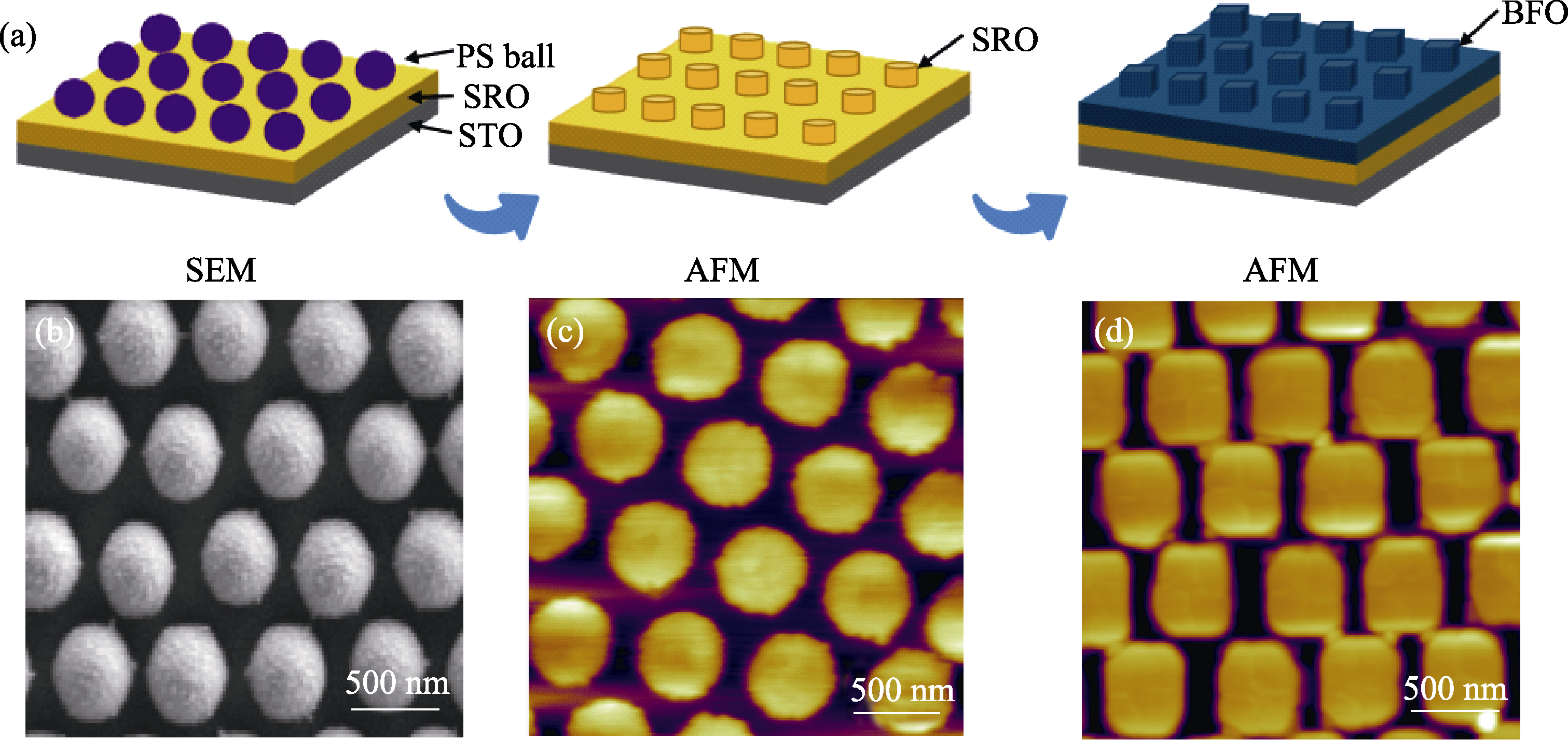
图1 (a)模板辅助生长法制备BFO纳米岛阵列流程示意图; (b~d)各阶段样品表面阵列形貌
Fig. 1 (a) Schematic diagram illustrating procedures of fabricating the BFO nanoisland arrays with templated growth strategy; (b-d) Images of sample surface at each fabrication stage
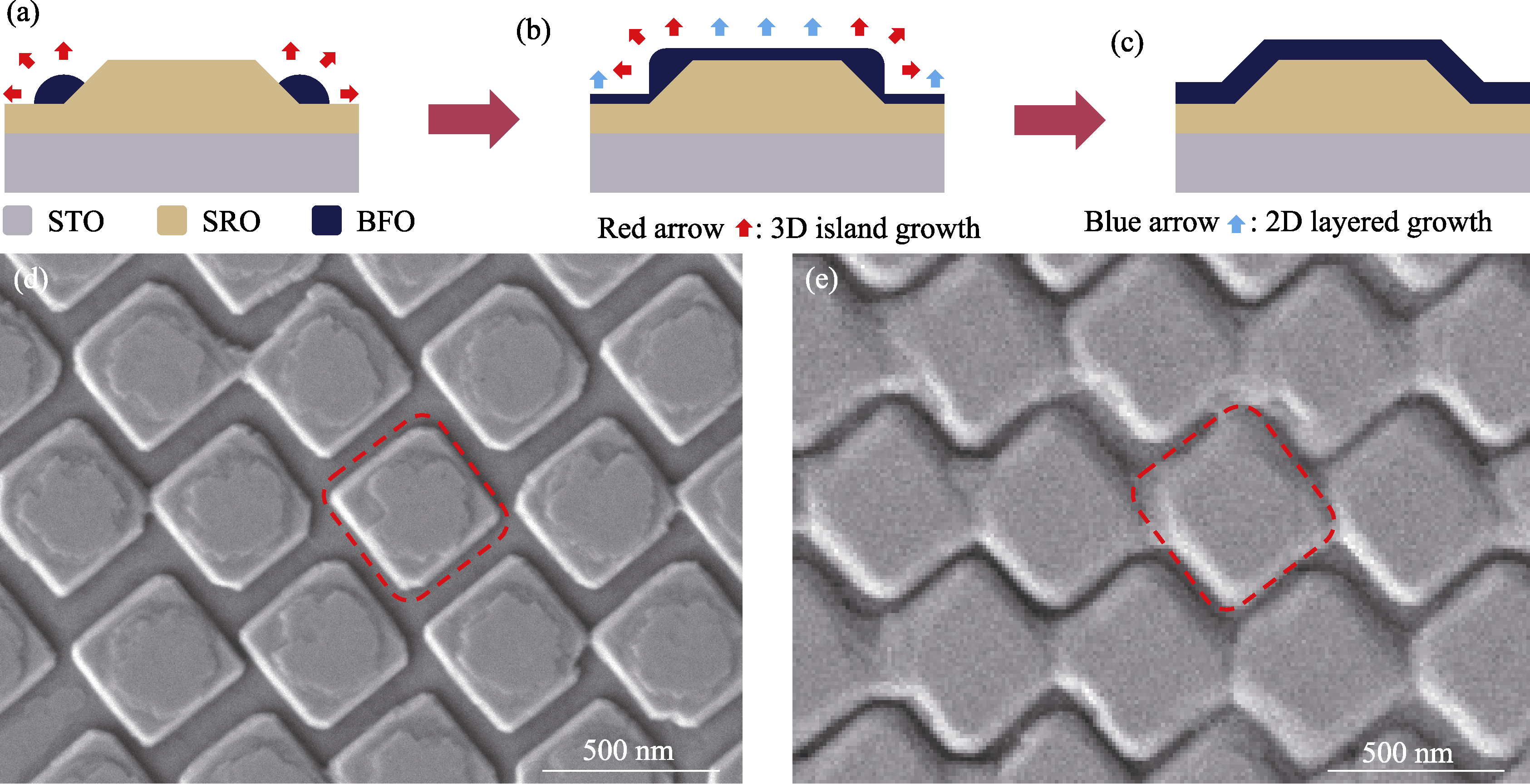
图2 BFO纳米岛阵列生长机理示意图
Fig. 2 Schematic illustration of the growth mechanism of BFO nanoislands (a) Preferential nucleation process of BFO during self-assembly; (b) Coexistence of two growth modes during the self-assembly process on the SRO nanoisland arrays; (c) Formation of self-assembled BFO nanoislands; (d) SEM image of growing ~30 nm of BFO nanoislands (corresponding to the growth stage in (b)); (e) SEM image of well-ordered BFO nanoisland arrays (corresponding to the growth stage in (c)). Colorful figures are available on website
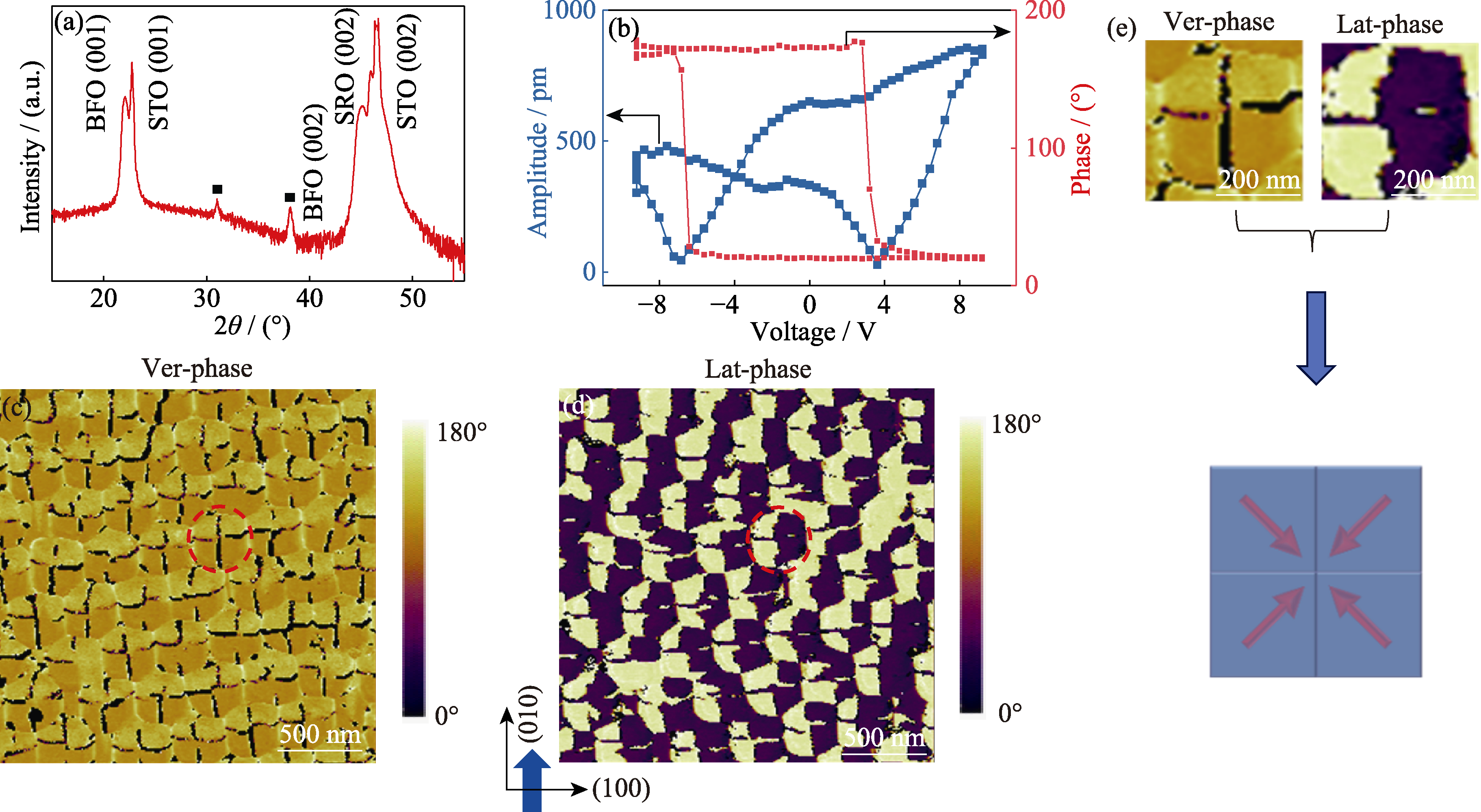
图3 BFO纳米岛阵列的晶体结构及拓扑畴分析
Fig. 3 Crystal structure and topological domain analysis of BFO nanoisland arrays (a) XRD pattern of BFO nanoisland arrays, where ■ denotes the impurity peaks generated in the substrate; (b) Piezoresponse hysteresis loops acquired on a randomly selected nanoisland exhibiting amplitude butterfly loop (blue) and phase hysteresis loop (red); (c, d) Vertical PFM phase image (c) and lateral PFM phase image (d) of BFO nanoisland arrays; (e) Schematic of 3D domain structures. Sample preparation conditions: 710 ℃, BFO thickness of 50 nm, SRO nanoisland height of 30 nm, and lateral size of 300 nm. Colorful figures are available on website
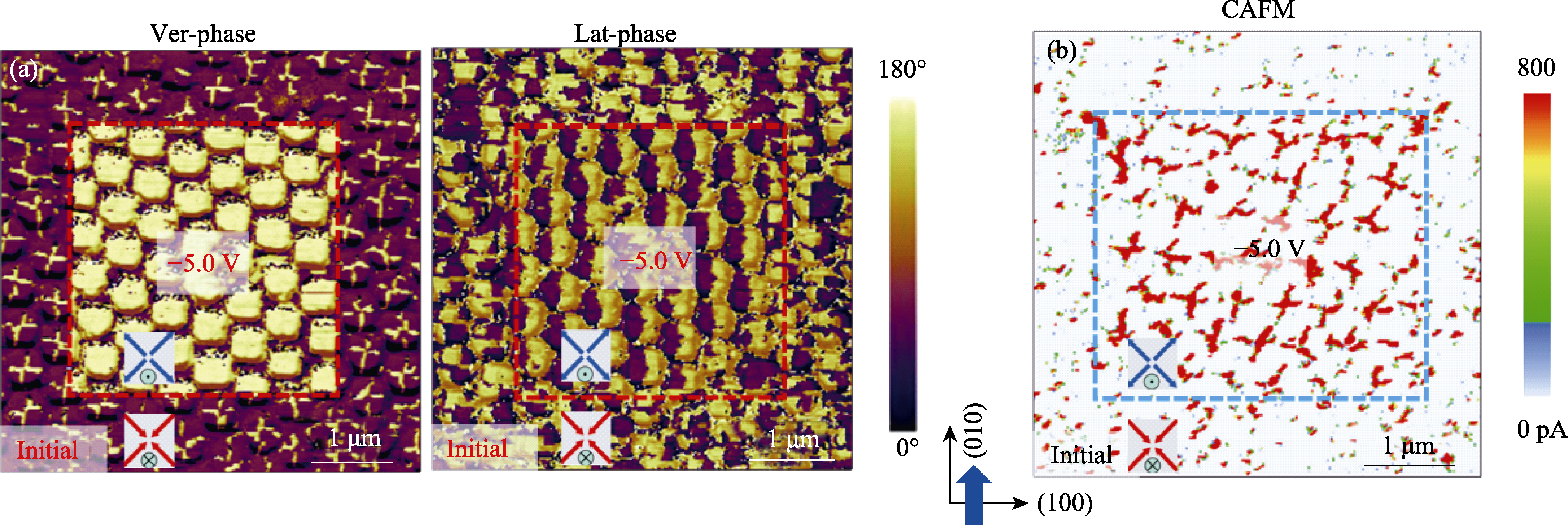
图4 BFO纳米岛阵列导电性调控
Fig. 4 Tunable conductivity in BFO nanoisland arrays (a) Phase images of the domain structures in BFO nanoislands before and after resistive switching between high-low resistance states, in which a write voltage of -5.0 V was applied within the red dashed box; (b) CAFM images of the nanoislands before and after resistive switching between high-low resistance states, in which a -5.0 V voltage is written in the blue dashed box. Sample preparation conditions: 710 ℃, BFO thickness of 50 nm, SRO nanoisland height of 30 nm, and lateral size of 300 nm. Colorful figures are available on website
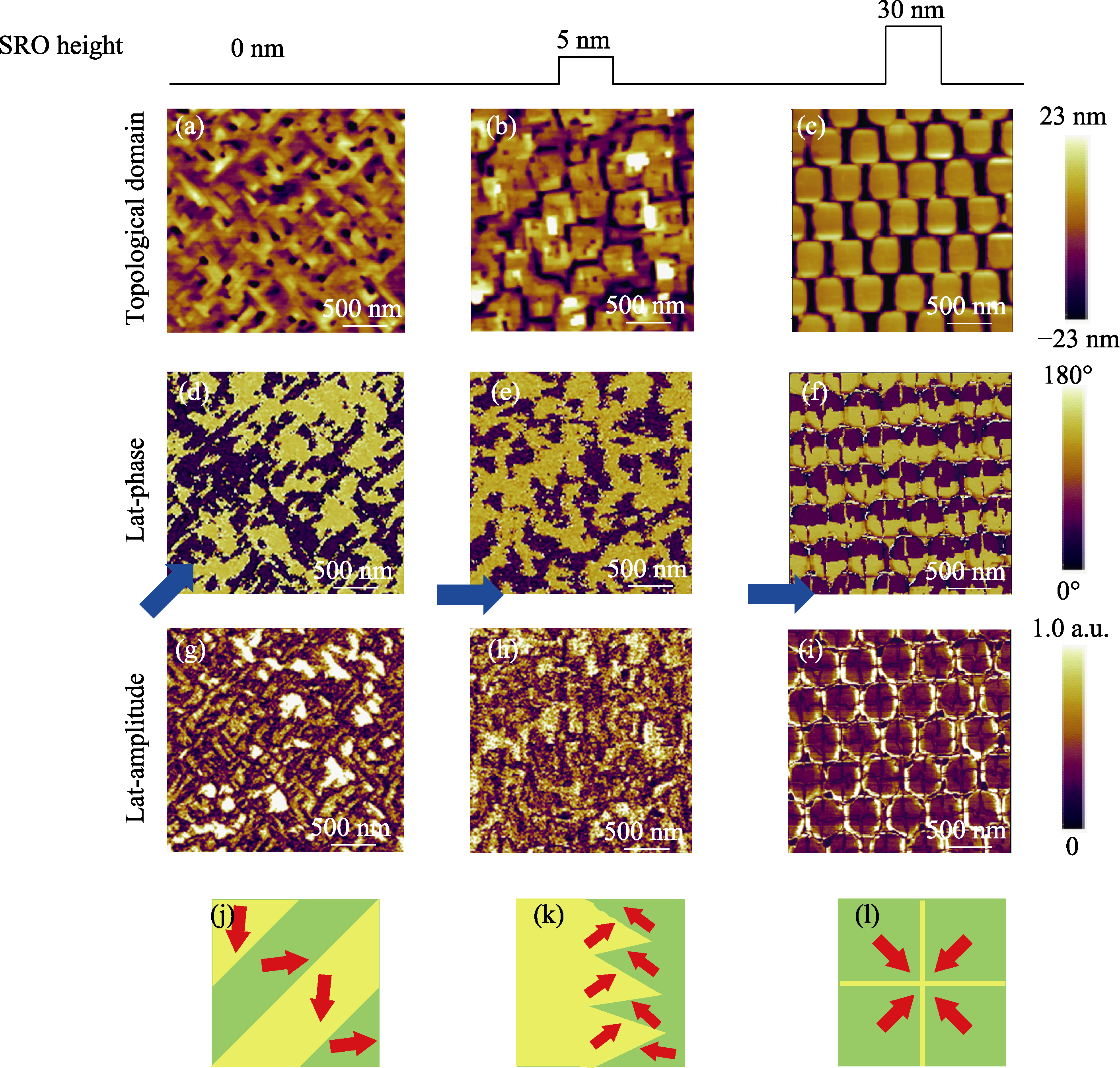
图5 SRO纳米岛高度对BFO纳米岛拓扑畴结构的影响
Fig. 5 Effect of SRO nanoisland height on the topological domain structure of BFO nanoislands (a-i) Morphologies (a-c), lat-phase (d-f) and lat-amplitude (g-i) PFM images of BFO nanoisland arrays analyzed as a function of SRO nanoisland height (0, 5 and 30 nm); (j-l) Schematic diagrams of different domain structures formed at heights of 0, 5 and 30 nm (from left to right), respectively. Colorful figures are available on website

图6 不同横向尺寸的SRO纳米岛对BFO纳米岛拓扑畴结构的影响
Fig. 6 Effect of lateral dimensions of SRO nanoislands on topological domain structure of BFO nanoislands (a-i) Morphologies (a-c), lat-phase (d-f) and ver-phase (g-i) PFM images of BFO nanoislands with varying lateral dimensions, including isolated BFO nanoislands with ~300 and ~500 nm diameters, as well as a wide BFO nanoisland chain of ~500 nm (from left to right); (j, k) Schematic diagrams of quad-domain texture and chain-shaped zigzag domain structure. Colorful figures are available on website
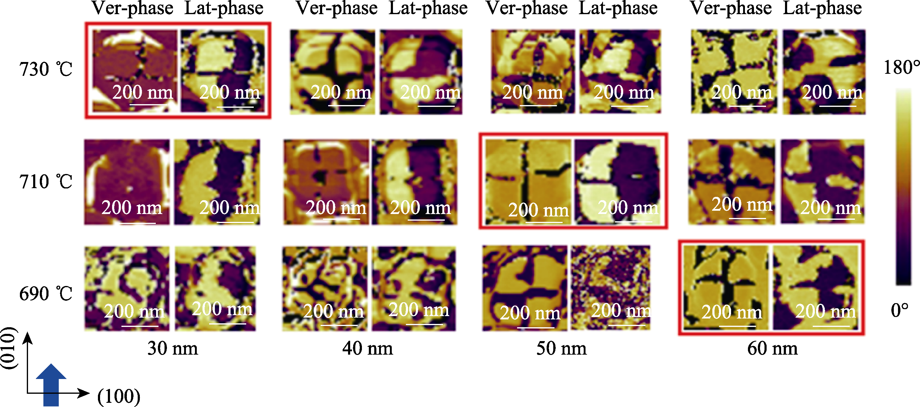
图7 厚度及生长温度对BFO纳米岛中心型畴结构的影响
Fig. 7 Effects of thickness and growth temperature on the central-type domain structure of BFO nanoislands PFM phase images of BFO nanoislands grown at 690, 710, and 730 ℃, with corresponding thickness gradients of 30, 40, 50, and 60 nm, respectively. Colorful figures are available on website
| [1] | SEIDEL J, VASUDEVAN R K, VALANOOR N. Topological structures in multiferroics-domain walls, skyrmions and vortices. Advanced Electronic Materials, 2016, 2(1): 1500292. |
| [2] | SEIDEL J. Nanoelectronics based on topological structures. Nature Materials, 2019, 18: 188. |
| [3] | DAS S, HONG Z, MCCARTER M, et al. A new era in ferroelectrics. APL Materials, 2020, 8(12): 120902. |
| [4] | TANG Y L, ZHU Y L, MA X L. Topological polar structures in ferroelectric oxide films. Journal of Applied Physics, 2021, 129(20): 200904. |
| [5] | TANG Y L, ZHU Y L, MA X L, et al. Observation of a periodic array of flux-closure quadrants in strained ferroelectric PbTiO3 films. Science, 2015, 348(6234): 547. |
| [6] | YADAV A K, NELSON C T, HSU S L, et al. Observation of polar vortices in oxide superlattices. Nature, 2016, 530: 198. |
| [7] | DAS S, TANG Y L, HONG Z, et al. Observation of room- temperature polar skyrmions. Nature, 2019, 568: 368. |
| [8] |
RODRIGUEZ B J, GAO X S, LIU L F, et al. Vortex polarization states in nanoscale ferroelectric arrays. Nano Letters, 2009, 9(3): 1127.
DOI PMID |
| [9] |
SCOTT J F. Applications of modern ferroelectrics. Science, 2007, 315(5814): 954.
PMID |
| [10] | OWCZAREK M, HUJSAK K A, FERRIS D P, et al. Flexible ferroelectric organic crystals. Nature Communications, 2016, 7: 13108. |
| [11] | MARTIN L W, RAPPE A M. Thin-film ferroelectric materials and their applications. Nature Reviews Materials, 2017, 2: 16087. |
| [12] | HAN S T, ZHOU Y, ROY V A L. Towards the development of flexible non-volatile memories. Advanced Materials, 2013, 25(38): 5424. |
| [13] | LI Z W, WANG Y J, TIAN G, et al. High-density array of ferroelectric nanodots with robust and reversibly switchable topological domain states. Science Advances, 2017, 3(8): e1700919. |
| [14] | KIM K E, JEONG S, CHU K, et al. Configurable topological textures in strain graded ferroelectric nanoplates. Nature Communications, 2018, 9: 403. |
| [15] | MA J, MA J, ZHANG Q H, et al. Controllable conductive readout in self-assembled, topologically confined ferroelectric domain walls. Nature Nanotechnology, 2018, 13: 947. |
| [16] | KIM K E, KIM Y J, ZHANG Y, et al. Ferroelastically protected polarization switching pathways to control electrical conductivity in strain-graded ferroelectric nanoplates. Physical Review Materials, 2018, 2: 084412. |
| [17] | HAN M J, WANG Y J, TANG Y L, et al. Shape and surface charge modulation of topological domains in oxide multiferroics. The Journal of Physical Chemistry C, 2019, 123(4): 2557. |
| [18] | DING L L, JI Y, ZHANG X Y, et al. Exotic quad-domain textures and transport characteristics of self-assembled BiFeO3 nanoislands on Nb-doped SrTiO3. ACS Applied Materials & Interfaces, 2021, 13(10): 12331. |
| [19] | ZHOU X, SUN H Y, LUO Z, et al. Ferroelectric diode characteristic and tri-state memory in self-assembled BiFeO3 nanoislands with cross-shaped domain structure. Applied Physics Letters, 2022, 121(4): 042903. |
| [20] | WANG Y, CHEN M F, MA J, et al. A self-assembly growth strategy for a highly ordered ferroelectric nanoisland array. Nanoscale, 2022, 14(38): 14046. |
| [21] | TIAN G, CHEN D Y, FAN H, et al. Observation of exotic domain structures in ferroelectric nanodot arrays fabricated via a universal nanopatterning approach. ACS Applied Materials & Interfaces, 2017, 9(42): 37219. |
| [22] | TIAN G, YI X, SONG Z Q, et al. Templated growth strategy for highly ordered topological ferroelectric quad-domain textures. Applied Physics Reviews, 2023, 10(2): 021413. |
| [23] | TIAN G, YANG W D, SONG X, et al. Manipulation of conductive domain walls in confined ferroelectric nanoislands. Advanced Functional Materials, 2019, 29(32): 1807276. |
| [24] |
ZHENG H M, ZHAN Q, ZAVALICHE F, et al. Controlling self-assembled perovskite-spinel nanostructures. Nano Letters, 2006, 6(7): 1401.
PMID |
| [25] | LI X L, WANG C X, YANG G W. Thermodynamic theory of growth of nanostructures. Progress in Materials Science, 2014, 64: 121. |
| [26] | PRESTIPINO S, LAIO A, TOSATTI E. Systematic improvement of classical nucleation theory. Physical Review Letters, 2012, 108(22): 225701. |
| [27] | LEE J K, CHOY J H, CHOI Y. Equilibrium shape and heterogeneous nucleation barrier at spherical interfaces. Surface Science, 1991, 256: 147. |
| [28] | GOMEZ L R, GARCIA N A, VITELLI V, et al. Phase nucleation in curved space. Nature Communications, 2015, 6: 6856. |
| [29] |
MA J, WANG J, ZHOU H, et al. Self-assembly growth of a multiferroic topological nanoisland array. Nanoscale, 2019, 11(43): 20514.
DOI PMID |
| [30] | WANG Z L. Steps and facets on annealed LaAlO3{100} and {110} surfaces. Surface Science, 1996, 360: 180. |
| [1] | 程澳芃, 王跃文, 许文涛, 刘全伟, 张海涛, 周有福. 吸附-沉淀自组装结合放电等离子烧结法制备石墨烯增强氧化铝复合陶瓷[J]. 无机材料学报, 2026, 41(4): 536-544. |
| [2] | 戴乐, 刘洋, 高轩, 王书豪, 宋雅婷, 唐明猛, 刘丽莎, 汪尧进. 浓度梯度掺杂实现BiFeO3薄膜自极化[J]. 无机材料学报, 2024, 39(1): 99-106. |
| [3] | 张祥松, 刘业通, 王永瑛, 武子瑞, 刘振中, 李毅, 杨娟. 自组装制备PtIr合金气凝胶及其高效电催化氨氧化性能[J]. 无机材料学报, 2023, 38(5): 511-520. |
| [4] | 李华鑫, 陈俊勇, 肖洲, 乐弦, 余显波, 向军辉. 纳米材料形貌和性能调控的仿生自组装研究进展[J]. 无机材料学报, 2021, 36(7): 695-710. |
| [5] | 李铁, 李玥, 王颖异, 张珽. 石墨烯-铁酸铋纳米晶复合材料的制备及其催化性能研究[J]. 无机材料学报, 2021, 36(7): 725-732. |
| [6] | 彭新村, 王智栋, 曾梦丝, 刘云, 邹继军, 朱志甫, 邓文娟. SiO2纳米球的粒径均一性研究及其在硅光学共振纳米柱阵列中的应用[J]. 无机材料学报, 2019, 34(7): 734-740. |
| [7] | 程国峰, 阮音捷, 孙玥, 尹晗迪. 纯相BiFeO3的热稳定和热膨胀性质研究[J]. 无机材料学报, 2019, 34(10): 1128-1133. |
| [8] | 程国峰, 阮音捷, 孙玥, 尹晗迪, 解其云. 元素配比对BiFeO3反应烧结相变影响的高温X射线衍射研究[J]. 无机材料学报, 2019, 34(10): 1035-1040. |
| [9] | 宋建民, 代秀红, 梁杰通, 赵磊, 周阳, 葛大勇, 孟旭东, 刘保亭. 偏轴磁控溅射法外延BiFeO3薄膜的介电性能与阻变效应[J]. 无机材料学报, 2018, 33(9): 1017-1021. |
| [10] | 王景平, 成方媛, 杜显锋, 徐友龙. 表面自组装法制备高比容Al2O3/TiO2复合膜[J]. 无机材料学报, 2018, 33(6): 617-622. |
| [11] | 范闻, 武利民. 硅油两步脱水法可控制备纳米二氧化钛透镜[J]. 无机材料学报, 2018, 33(12): 1337-1342. |
| [12] | 罗 维, 魏 晶, 邓勇辉, 李宇慧, 王连军, 赵 涛, 江 莞. 新型两亲性嵌段共聚物导向合成有序大孔径介孔材料的研究进展[J]. 无机材料学报, 2017, 32(1): 1-10. |
| [13] | 武萱蓉, 杨巧珍, 赵永祥, 路艳罗. ZnS微球的水热/溶剂热法合成及其光催化性能研究[J]. 无机材料学报, 2016, 31(5): 473-478. |
| [14] | 张文强, 张 锌. 厘米级盘形硅藻微粒单层密排研究[J]. 无机材料学报, 2015, 30(11): 1208-1212. |
| [15] | 孙志娟, 陈雪莲, 蒋春跃. 自组装法制备中空二氧化硅纳米粒子减反射薄膜[J]. 无机材料学报, 2014, 29(9): 947-955. |
| 阅读次数 | ||||||
|
全文 |
|
|||||
|
摘要 |
|
|||||